
ATV303_Introduction_OPP (NXPowerLite)
- 格式:ppt
- 大小:578.00 KB
- 文档页数:37

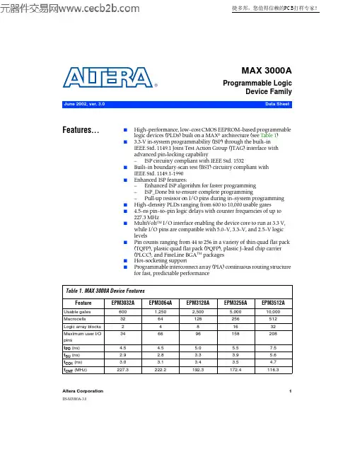
®Altera Corporation 1MAX 3000AProgrammable Logic Device FamilyJune 2002, ver. 3.0Data Sheet DS-M3000A-3.0Features...■High–performance, low–cost CMOS EEPROM–based programmable logic devices (PLDs) built on a MAX ® architecture (see Table 1)■3.3-V in-system programmability (ISP) through the built–in IEEE Std. 1149.1 Joint Test Action Group (JTAG) interface with advanced pin-locking capability –ISP circuitry compliant with IEEE Std. 1532■Built–in boundary-scan test (BST) circuitry compliant with IEEE Std. 1149.1-1990■Enhanced ISP features:–Enhanced ISP algorithm for faster programming –ISP_Done bit to ensure complete programming –Pull-up resistor on I/O pins during in–system programming ■High–density PLDs ranging from 600 to 10,000 usable gates ■4.5–ns pin–to–pin logic delays with counter frequencies of up to 227.3MHz ■MultiVolt TM I/O interface enabling the device core to run at 3.3 V, while I/O pins are compatible with 5.0–V, 3.3–V, and 2.5–V logic levels ■Pin counts ranging from 44 to 256 in a variety of thin quad flat pack (TQFP), plastic quad flat pack (PQFP), plastic J–lead chip carrier (PLCC), and FineLine BGA TM packages ■Hot–socketing support ■Programmable interconnect array (PIA) continuous routing structurefor fast, predictable performance Table 1.MAX3000A Device Features FeatureEPM3032A EPM3064A EPM3128A EPM3256A EPM3512A Usable gates6001,2502,5005,00010,000Macrocells3264128256512Logic array blocks2481632Maximum user I/Opins346696158208t PD (ns)4.5 4.55.0 5.57.5t SU (ns)2.9 2.83.3 3.9 5.6t CO1 (ns)3.0 3.1 3.4 3.54.7f CNT (MHz)227.3222.2192.3172.4116.3捷多邦,您值得信赖的PCB打样专家!MAX 3000A Programmable Logic Device Family Data Sheet...and More Features ■PCI compatible■Bus–friendly architecture including programmable slew–rate control ■Open–drain output option■Programmable macrocell flipflops with individual clear, preset, clock, and clock enable controls■Programmable power–saving mode for a power reduction of over 50% in each macrocell■Configurable expander product–term distribution, allowing up to32 product terms per macrocell■Programmable security bit for protection of proprietary designs■Enhanced architectural features, including:– 6 or 10 pin– or logic–driven output enable signals–Two global clock signals with optional inversion–Enhanced interconnect resources for improved routability–Programmable output slew–rate control■Software design support and automatic place–and–route provided by Altera’s development systems for Windows–based PCs and Sun SPARCstations, and HP 9000 Series 700/800 workstations■Additional design entry and simulation support provided by EDIF2 0 0 and3 0 0 netlist files, library of parameterized modules (LPM),Verilog HDL, VHDL, and other interfaces to popular EDA tools from third–party manufacturers such as Cadence, Exemplar Logic, Mentor Graphics, OrCAD, Synopsys, Synplicity, and VeriBest■Programming support with the Altera master programming unit (MPU), MasterBlaster TM communications cable, ByteBlasterMV TMparallel port download cable, BitBlaster TM serial download cable as well as programming hardware from third–party manufacturers and any in–circuit tester that supports Jam TM Standard Test andProgramming Language (STAPL) Files (.jam), Jam STAPL Byte-Code Files (.jbc), or Serial Vector Format Files (.svf)General Description MAX3000A devices are low–cost, high–performance devices based on the Altera MAX architecture. Fabricated with advanced CMOS technology, the EEPROM–based MAX3000A devices operate with a 3.3-V supply voltage and provide 600 to 10,000 usable gates, ISP, pin-to-pin delays as fast as 4.5 ns, and counter speeds of up to 227.3MHz. MAX3000A devices in the –4, –5, –6, –7, and –10 speed grades are compatible with the timing requirements of the PCI Special Interest Group (PCI SIG) PCI Local Bus Specification, Revision2.2. See Table2.2Altera CorporationAltera Corporation 3MAX 3000A Programmable Logic Device Family Data Sheet The MAX 3000A architecture supports 100% transistor-to-transistor logic (TTL) emulation and high–density small-scale integration (SSI), medium-scale integration (MSI), and large-scale integration (LSI) logic functions. The MAX 3000A architecture easily integrates multiple devices ranging from PALs, GALs, and 22V10s to MACH and pLSI devices. MAX 3000A devices are available in a wide range of packages, including PLCC, PQFP, and TQFP packages. See Table 3.Note:(1)When the IEEE Std. 1149.1 (JTAG) interface is used for in–system programming or boundary–scan testing, four I/O pins become JTAG pins.MAX 3000A devices use CMOS EEPROM cells to implement logic functions. The user–configurable MAX 3000A architecture accommodates a variety of independent combinatorial and sequential logic functions. The devices can be reprogrammed for quick and efficient iterations during design development and debugging cycles, and can be programmed and erased up to 100 times.Table 2.MAX 3000A Speed Grades Device Speed Grade –4–5–6–7–10EPM3032A v v v EPM3064A vv v EPM3128A v v v EPM3256A v v EPM3512A v v Table 3.MAX 3000A Maximum User I/O Pins Note (1)Device 44–Pin PLCC 44–Pin TQFP 100–Pin TQFP 144–Pin TQFP 208–Pin PQFP 256-Pin FineLine BGA EPM3032A 3434EPM3064A 343466EPM3128A 8096EPM3256A 116158EPM3512A 172208MAX 3000A Programmable Logic Device Family Data SheetMAX3000A devices contain 32 to 512 macrocells, combined into groupsof 16 macrocells called logic array blocks (LABs). Each macrocell has aprogrammable–AND/fixed–OR array and a configurable register withindependently programmable clock, clock enable, clear, and presetfunctions. To build complex logic functions, each macrocell can besupplemented with shareable expander and high–speed parallelexpander product terms to provide up to 32 product terms per macrocell.MAX3000A devices provide programmable speed/power optimization.Speed–critical portions of a design can run at high speed/full power,while the remaining portions run at reduced speed/low power. Thisspeed/power optimization feature enables the designer to configure oneor more macrocells to operate at 50% or lower power while adding only anominal timing delay. MAX3000A devices also provide an option thatreduces the slew rate of the output buffers, minimizing noise transientswhen non–speed–critical signals are switching. The output drivers of allMAX3000A devices can be set for 2.5V or 3.3V, and all input pins are2.5–V,3.3–V, and 5.0-V tolerant, allowing MAX3000A devices to be usedin mixed–voltage systems.MAX3000A devices are supported by Altera development systems,which are integrated packages that offer schematic, text—includingVHDL, Verilog HDL, and the Altera Hardware Description Language(AHDL)—and waveform design entry, compilation and logic synthesis,simulation and timing analysis, and device programming. The softwareprovides EDIF 2 0 0 and 3 0 0, LPM, VHDL, Verilog HDL, and otherinterfaces for additional design entry and simulation support from otherindustry–standard PC– and UNIX–workstation–based EDA tools. Thesoftware runs on Windows–based PCs, as well as Sun SPARCstation, andHP 9000 Series 700/800 workstations.f For more information on development tools, see the MAX+PLUS IIProgrammable Logic Development System & Software Data Sheet andtheQuartus Programmable Logic Development System & Software Data Sheet.Functional Description The MAX3000A architecture includes the following elements:■Logic array blocks (LABs)■Macrocells■Expander product terms (shareable and parallel)■Programmable interconnect array (PIA)■I/O control blocksThe MAX3000A architecture includes four dedicated inputs that can be used as general–purpose inputs or as high–speed, global control signals (clock, clear, and two output enable signals) for each macrocell and I/O pin. Figure1 shows the architecture of MAX3000A devices.4Altera CorporationMAX 3000A Programmable Logic Device Family Data Sheet Figure 1. MAX3000A Device Block DiagramNote:(1)EPM3032A, EPM3064A, EPM3128A, and EPM3256A devices have six output enables. EPM3512A devices have10output enables.Logic Array BlocksThe MAX3000A device architecture is based on the linking ofhigh–performance LABs. LABs consist of 16–macrocell arrays, as shownin Figure1. Multiple LABs are linked together via the PIA, a global busthat is fed by all dedicated input pins, I/O pins, and macrocells.Each LAB is fed by the following signals:■36 signals from the PIA that are used for general logic inputs■Global controls that are used for secondary register functionsAltera Corporation 5MAX 3000A Programmable Logic Device Family Data SheetMacrocellsMAX3000A macrocells can be individually configured for eithersequential or combinatorial logic operation. Macrocells consist of threefunctional blocks: logic array, product–term select matrix, andprogrammable register. Figure2 shows a MAX3000A macrocell.Figure 2. MAX3000A MacrocellQCLRNTo PIACombinatorial logic is implemented in the logic array, which providesfive product terms per macrocell. The product–term select matrixallocates these product terms for use as either primary logic inputs (to theOR and XOR gates) to implement combinatorial functions, or as secondaryinputs to the macrocell’s register preset, clock, and clock enable controlfunctions.Two kinds of expander product terms (“expanders”) are available tosupplement macrocell logic resources:■Shareable expanders, which are inverted product terms that are fedback into the logic array■Parallel expanders, which are product terms borrowed from adjacentmacrocellsThe Altera development system automatically optimizes product–termallocation according to the logic requirements of the design.6Altera CorporationMAX 3000A Programmable Logic Device Family Data SheetFor registered functions, each macrocell flipflop can be individuallyprogrammed to implement D, T, JK, or SR operation with programmableclock control. The flipflop can be bypassed for combinatorial operation.During design entry, the designer specifies the desired flipflop type; theAltera development system software then selects the most efficientflipflop operation for each registered function to optimize resourceutilization.Each programmable register can be clocked in three different modes:■Global clock signal mode, which achieves the fastest clock–to–outputperformance.■Global clock signal enabled by an active–high clock enable. A clockenable is generated by a product term. This mode provides an enableon each flipflop while still achieving the fast clock–to–outputperformance of the global clock.■Array clock implemented with a product term. In this mode, theflipflop can be clocked by signals from buried macrocells or I/O pins.Two global clock signals are available in MAX3000A devices. As shownin Figure1, these global clock signals can be the true or the complement ofeither of the two global clock pins, GCLK1 or GCLK2.Each register also supports asynchronous preset and clear functions. Asshown in Figure2, the product–term select matrix allocates product termsto control these operations. Although the product–term–driven presetand clear from the register are active high, active–low control can beobtained by inverting the signal within the logic array. In addition, eachregister clear function can be individually driven by the active–lowdedicated global clear pin (GCLRn).Expander Product TermsAlthough most logic functions can be implemented with the five productterms available in each macrocell, highly complex logic functions requireadditional product terms. Another macrocell can be used to supply therequired logic resources. However, the MAX3000A architecture alsooffers both shareable and parallel expander product terms (“expanders”)that provide additional product terms directly to any macrocell in thesame LAB. These expanders help ensure that logic is synthesized with thefewest possible logic resources to obtain the fastest possible speed. Altera Corporation 78Altera Corporation MAX 3000A Programmable Logic Device Family Data SheetShareable Expanders Each LAB has 16 shareable expanders that can be viewed as a pool of uncommitted single product terms (one from each macrocell) with inverted outputs that feed back into the logic array. Each shareable expander can be used and shared by any or all macrocells in the LAB to build complex logic functions. Shareable expanders incur a small delay (t SEXP ). Figure 3 shows how shareable expanders can feed multiple macrocells.Figure 3. MAX 3000A Shareable Expanders Shareable expanders can be shared by any or all macrocells in an LAB.Parallel Expanders Parallel expanders are unused product terms that can be allocated to a neighboring macrocell to implement fast, complex logic functions. Parallel expanders allow up to 20 product terms to directly feed the macrocell OR logic, with five product terms provided by the macrocell and 15 parallel expanders provided by neighboring macrocells in the LAB. MacrocellProduct-Term Logic Product-Term Select Matrix Macrocell Product-Term Logic 36 Signals from PIA 16 Shared ExpandersMAX 3000A Programmable Logic Device Family Data SheetThe Altera development system compiler can automatically allocate up tothree sets of up to five parallel expanders to the macrocells that requireadditional product terms. Each set of five parallel expanders incurs asmall, incremental timing delay (t PEXP). For example, if a macrocellrequires 14product terms, the compiler uses the five dedicated productterms within the macrocell and allocates two sets of parallel expanders;the first set includes five product terms, and the second set includes fourproduct terms, increasing the total delay by 2 ×t PEXP.Two groups of eight macrocells within each LAB (e.g., macrocells 1through 8 and 9through 16) form two chains to lend or borrow parallelexpanders. A macrocell borrows parallel expanders from lower–numbered macrocells. For example, macrocell 8 can borrow parallelexpanders from macrocell 7, from macrocells 7 and 6, or from macrocells7, 6, and 5. Within each group of eight, the lowest–numbered macrocellcan only lend parallel expanders and the highest–numbered macrocell canonly borrow them. Figure4 shows how parallel expanders can beborrowed from a neighboring macrocell.Figure 4. MAX3000A Parallel ExpandersUnused product terms in a macrocell can be allocated to a neighboring macrocell.Altera Corporation 9MAX 3000A Programmable Logic Device Family Data SheetProgrammable Interconnect ArrayLogic is routed between LABs on the PIA. This global bus is aprogrammable path that connects any signal source to any destination onthe device. All MAX3000A dedicated inputs, I/O pins, and macrocelloutputs feed the PIA, which makes the signals available throughout theentire device. Only the signals required by each LAB are actually routedfrom the PIA into the LAB. Figure5 shows how the PIA signals are routedinto the LAB. An EEPROM cell controls one input to a two-input AND gate,which selects a PIA signal to drive into the LAB.Figure 5. MAX3000A PIA RoutingWhile the routing delays of channel–based routing schemes in masked orFPGAs are cumulative, variable, and path–dependent, the MAX3000APIA has a predictable delay. The PIA makes a design’s timingperformance easy to predict.I/O Control BlocksThe I/O control block allows each I/O pin to be individually configuredfor input, output, or bidirectional operation. All I/O pins have a tri–statebuffer that is individually controlled by one of the global output enablesignals or directly connected to ground or V CC. Figure6 shows the I/Ocontrol block for MAX3000A devices. The I/O control block has 6 or10global output enable signals that are driven by the true or complementof two output enable signals, a subset of the I/O pins, or a subset of theI/O macrocells.10Altera CorporationMAX 3000A Programmable Logic Device Family Data Sheet Figure 6. I/O Control Block of MAX3000A DevicesNote:(1)EPM3032A, EPM3064A, EPM3128A, and EPM3256A devices have six output enables. EPM3512A devices have10output enables.When the tri–state buffer control is connected to ground, the output istri-stated (high impedance), and the I/O pin can be used as a dedicatedinput. When the tri–state buffer control is connected to V CC, the output isenabled.The MAX3000A architecture provides dual I/O feedback, in whichmacrocell and pin feedbacks are independent. When an I/O pin isconfigured as an input, the associated macrocell can be used for buriedlogic.Altera Corporation 1112Altera Corporation MAX 3000A Programmable Logic Device Family Data SheetIn–SystemProgramma-bilityMAX 3000A devices can be programmed in–system via an industry–standard four–pin IEEE Std. 1149.1-1990 (JTAG) interface. In-system programmability (ISP) offers quick, efficient iterations during design development and debugging cycles. The MAX 3000A architecture internally generates the high programming voltages required to program its EEPROM cells, allowing in–system programming with only a single 3.3–V power supply. During in–system programming, the I/O pins are tri–stated and weakly pulled–up to eliminate board conflicts. The pull–up value is nominally 50 k Ω.MAX 3000A devices have an enhanced ISP algorithm for faster programming. These devices also offer an ISP_Done bit that ensures safe operation when in–system programming is interrupted. This ISP_Done bit, which is the last bit programmed, prevents all I/O pins from driving until the bit is programmed.ISP simplifies the manufacturing flow by allowing devices to be mounted on a printed circuit board (PCB) with standard pick–and–place equipment before they are programmed. MAX 3000A devices can be programmed by downloading the information via in–circuit testers, embedded processors, the MasterBlaster communications cable, the ByteBlasterMV parallel port download cable, and the BitBlaster serial download cable. Programming the devices after they are placed on the board eliminates lead damage on high–pin–count packages (e.g., QFP packages) due to device handling. MAX 3000A devices can be reprogrammed after a system has already shipped to the field. For example, product upgrades can be performed in the field via software or modem. The Jam STAPL programming and test language can be used to program MAX 3000A devices with in–circuit testers, PCs, or embedded processors.fFor more information on using the Jam STAPL programming and test language, see Application Note 88 (Using the Jam Language for ISP & ICR via an Embedded Processor), Application Note 122 (Using Jam STAPL for ISP & ICR via an Embedded Processor) and AN 111 (Embedded Programming Using the 8051 and Jam Byte-Code).The ISP circuitry in MAX 3000A devices is compliant with the IEEE Std. 1532 specification. The IEEE Std. 1532 is a standard developed to allow concurrent ISP between multiple PLD vendors.Programmingwith ExternalHardwareMAX 3000A devices can be programmed on Windows–based PCs with an Altera Logic Programmer card, MPU, and the appropriate device adapter. The MPU performs continuity checking to ensure adequate electrical contact between the adapter and the device. fFor more information, see the Altera Programming Hardware Data Sheet.Altera Corporation 13MAX 3000A Programmable Logic Device Family Data SheetThe Altera software can use text– or waveform–format test vectors createdwith the Altera Text Editor or Waveform Editor to test the programmeddevice. For added design verification, designers can perform functionaltesting to compare the functional device behavior with the results ofsimulation.Data I/O, BP Microsystems, and other programming hardwaremanufacturers also provide programming support for Altera devices.fFor more information, see Programming Hardware Manufacturers .IEEE Std.1149.1 (JTAG)Boundary–ScanSupport MAX 3000A devices include the JTAG BST circuitry defined by IEEE Std.1149.1–1990. Table 4 describes the JTAG instructions supported by MAX 3000A devices. The pin-out tables found on the Altera web site ( ) or the Altera Digital Library show the location of the JTAG control pins for each device. If the JTAG interface is notrequired, the JTAG pins are available as user I/O pins.The instruction register length of MAX 3000A devices is 10 bits. TheIDCODE and USERCODE register length is 32 bits. Tables 5 and 6 showthe boundary–scan register length and device IDCODE information forMAX 3000A devices.Table 4.MAX 3000A JTAG InstructionsJTAG InstructionDescription SAMPLE/PRELOADAllows a snapshot of signals at the device pins to be captured and examined during normal device operation, and permits an initial data pattern output at the device pins EXTESTAllows the external circuitry and board–level interconnections to be tested by forcing a test pattern at the output pins and capturing test results at the input pins BYPASS Places the 1–bit bypass register between the TDI and TDO pins, which allows the BSTdata to pass synchronously through a selected device to adjacent devices during normaldevice operationIDCODE Selects the IDCODE register and places it between the TDI and TDO pins, allowing theIDCODE to be serially shifted out of TDOUSERCODE Selects the 32–bit USERCODE register and places it between the TDI and TDO pins,allowing the USERCODE value to be shifted out of TDOISP InstructionsThese instructions are used when programming MAX 3000A devices via the JTAG portswith the MasterBlaster, ByteBlasterMV, or BitBlaster cable, or when using a Jam STAPLfile, JBC file, or SVF file via an embedded processor or test equipment14Altera Corporation MAX 3000A Programmable Logic Device Family Data SheetNotes:(1)The most significant bit (MSB) is on the left.(2)The least significant bit (LSB) for all JTAG IDCODEs is 1.fSee Application Note 39 (IEEE 1149.1 (JTAG) Boundary–Scan Testing in Altera Devices) for more information on JTAG BST.Table 5.MAX 3000A Boundary–Scan Register Length Device Boundary–Scan Register Length EPM3032A 96EPM3064A 192EPM3128A 288EPM3256A 480EPM3512A 624Table 6.32–Bit MAX 3000A Device IDCODE Value Note (1)Device IDCODE (32 bits)Version (4 Bits)Part Number (16 Bits) Manufacturer’s Identity (11 Bits) 1 (1 Bit) (2)EPM3032A 00010111 0000 0011 0010000011011101EPM3064A 00010111 0000 0110 0100000011011101EPM3128A 00010111 0001 0010 1000000011011101EPM3256A 00010111 0010 0101 0110000011011101EPM3512A 00010111 0101 0001 0010000011011101MAX 3000A Programmable Logic Device Family Data SheetFigure7 shows the timing information for the JTAG signals.Figure 7. MAX3000A JTAG WaveformsTable7 shows the JTAG timing parameters and values for MAX3000Adevices.Table 7.JTAG Timing Parameters & Values for MAX3000A DevicesSymbol Parameter Min Max Unitt JCP TCK clock period 100nst JCH TCK clock high time 50nst JCL TCK clock low time 50nst JPSU JTAG port setup time 20nst JPH JTAG port hold time 45nst JPCO JTAG port clock to output25nst JPZX JTAG port high impedance to valid output25nst JPXZ JTAG port valid output to high impedance25nst JSSU Capture register setup time20nst JSH Capture register hold time45nst JSCO Update register clock to output25nst JSZX Update register high impedance to valid output25nst JSXZ Update register valid output to high impedance25ns Altera Corporation 15MAX 3000A Programmable Logic Device Family Data SheetProgrammable Speed/Power Control MAX3000A devices offer a power–saving mode that supports low-power operation across user–defined signal paths or the entire device. This feature allows total power dissipation to be reduced by 50% or more because most logic applications require only a small fraction of all gates to operate at maximum frequency.The designer can program each individual macrocell in a MAX3000A device for either high–speed or low–power operation. As a result, speed-critical paths in the design can run at high speed, while the remaining paths can operate at reduced power. Macrocells that run at low power incur a nominal timing delay adder (t LPA) for the t LAD, t LAC, t IC, t ACL, t EN, t CPPW and t SEXP parameters.Output Configuration MAX3000A device outputs can be programmed to meet a variety of system–level requirements.MultiVolt I/O InterfaceThe MAX3000A device architecture supports the MultiVolt I/O interface feature, which allows MAX3000A devices to connect to systems with differing supply voltages. MAX3000A devices in all packages can be set for 2.5–V, 3.3–V, or 5.0–V I/O pin operation. These devices have one set of V CC pins for internal operation and input buffers (VCCINT), and another set for I/O output drivers (VCCIO).The VCCIO pins can be connected to either a 3.3–V or 2.5–V power supply, depending on the output requirements. When the VCCIO pins are connected to a 2.5–V power supply, the output levels are compatible with 2.5–V systems. When the VCCIO pins are connected to a 3.3–V power supply, the output high is at 3.3V and is therefore compatible with 3.3-V or 5.0–V systems. Devices operating with V CCIO levels lower than 3.0V incur a nominally greater timing delay of t OD2 instead of t OD1. Inputs can always be driven by 2.5–V, 3.3–V, or 5.0–V signals.Table8 summarizes the MAX3000A MultiVolt I/O support.Note:(1)When V CCIO is 3.3 V, a MAX 3000A device can drive a 2.5–V device that has 3.3–Vtolerant inputs.Table 8.MAX3000A MultiVolt I/O SupportV CCIO Voltage Input Signal (V)Output Signal (V)2.53.3 5.0 2.5 3.3 5.02.5v v v v3.3v v v v v v16Altera CorporationMAX 3000A Programmable Logic Device Family Data SheetOpen–Drain Output OptionMAX3000A devices provide an optional open–drain (equivalent toopen-collector) output for each I/O pin. This open–drain output enablesthe device to provide system–level control signals (e.g., interrupt andwrite enable signals) that can be asserted by any of several devices. It canalso provide an additional wired–OR plane.Open-drain output pins on MAX3000A devices (with a pull-up resistor tothe 5.0-V supply) can drive 5.0-V CMOS input pins that require a high V IH.When the open-drain pin is active, it will drive low. When the pin isinactive, the resistor will pull up the trace to 5.0V, thereby meeting CMOSrequirements. The open-drain pin will only drive low or tri-state; it willnever drive high. The rise time is dependent on the value of the pull-upresistor and load impedance. The I OL current specification should beconsidered when selecting a pull-up resistorSlew–Rate ControlThe output buffer for each MAX3000A I/O pin has an adjustable outputslew rate that can be configured for low–noise or high–speedperformance. A faster slew rate provides high–speed transitions forhigh-performance systems. However, these fast transitions may introducenoise transients into the system. A slow slew rate reduces system noise,but adds a nominal delay of 4 to 5 ns. When the configuration cell isturned off, the slew rate is set for low–noise performance. Each I/O pinhas an individual EEPROM bit that controls the slew rate, allowingdesigners to specify the slew rate on a pin–by–pin basis. The slew ratecontrol affects both the rising and falling edges of the output signal. Design Security All MAX3000A devices contain a programmable security bit that controlsaccess to the data programmed into the device. When this bit isprogrammed, a design implemented in the device cannot be copied orretrieved. This feature provides a high level of design security becauseprogrammed data within EEPROM cells is invisible. The security bit thatcontrols this function, as well as all other programmed data, is reset onlywhen the device is reprogrammed.Generic Testing MAX3000A devices are fully tested. Complete testing of eachprogrammable EEPROM bit and all internal logic elements ensures 100%programming yield. AC test measurements are taken under conditionsequivalent to those shown in Figure8. Test patterns can be used and thenerased during early stages of the production flow.Altera Corporation 17。

GENERAL DESCRIPTIONOB2279 is a highly integrated current mode PWM control IC optimized for high performance, low standby power and cost effective offline flyback converter applications. PWM switching frequency at normal operation is externally programmable and trimmed to tight range. At no load or light load condition, the IC operates in extended ‘burst mode’ to minimize switching loss. Lower standby power and higher conversion efficiency is thus achieved. VDD low startup current and low operating current contribute to a reliable power on startup design with OB2279. A large value resistor could thus be used in the startup circuit for reduced power loss. The internal slope compensation improves system large signal stability and reduces the possible sub-harmonic oscillation at high PWM duty cycle output. Leading-edge blanking on current sense input removes the signal glitch due to snubber circuit diode reverse recovery and greatly reduces the externalcomponent count and system cost in the design.OB2279 offers comprehensive protection coverageincluding Cycle-by-Cycle current limiting(OCP),VDD Under Voltage Lockout(UVLO), VDD OverVoltage Protection(OVP), VDD Clamp, Gate Clamp,Over Load protection(OLP) and Over Temperatureprotection (OTP), etc.Different latch shutdown options are offered onOB2279 in different device version. V version has OVP Latch shutdown. T version supports both OVP and OTP latch shutdown. L version provides all OVP, OTP and OLP latch shutdown control. Excellent EMI performance is achieved with On-Bright proprietary frequency shuffling technique together with soft switching control at the totem pole gate drive output. Tone energy at below 20KHZ is minimized in operation. Consequently, audio noise is eliminated during operation.OB2279 is offered in SOP-8 and DIP-8 packages.FEATURES■ On-Bright Proprietary Frequency Shuffling Technology for Improved EMI Performance ■ Power On Soft Start■ Extended Burst Mode Control For Improved Efficiency and Minimum Standby Power Design ■ Audio Noise Free Operation■ External Programmable PWM Switching Frequency ■ Internal Synchronized Slope Compensation■ Low VIN/VDD Startup Current(3uA) and Low Operating Current (2.3mA)■ Leading Edge Blanking on Current Sense Input ■ Complete Protection Coverage with selective protections for Latch Shutdown o VDD Over Voltage Protection(OVP) – LatchShutdown o Over Temperature Protection(OTP) – Auto recovery or Latch Shutdowno Over Load Protection. (OLP) – Auto recovery or Latch Shutdown o VDD Under Voltage Lockout with Hysteresis (UVLO) o Gate Output Voltage Clamp (16.5V) o Built-in OCP Compensation to Achieve Minimum OPP Variation over Universal AC Input Range. APPLICATIONSOffline AC/DC flyback converter for ■ Adaptor ■ Notebook Adaptor ■ LCD Monitor/TV/PC/Set-Top Box PowerSupplies■ Open-frame SMPS ■ Printer Power TYPICAL APPLICATIONOn -B ri g h tC o nf i de n ti al ToH ig hr ayGENERAL INFORMATIONPin ConfigurationThe pin map of OB2279 in DIP8 and SOP8 package is shown as below.Ordering Information Part Number Description OB2279AP-V DIP8, V version with OVPLatchOB2279AP-T DIP8, T version withOVP/OTP latchOB2279AP-L DIP8, L version withOVP/OTP/OLP latchOB2279CP-V SOP8, V version with OVPlatchOB2279CP-T SOP8, T version withOVP/OTP latchOB2279CP-LSOP8, L version with OVP/OTP/OLP latchNote: All Devices are offered in Pb-free Package if not otherwisenoted.Package Dissipation Rating PackageR θJA (°C/W)DIP8 90 SOP8 150Absolute Maximum RatingsParameter Value VDD Clamp Voltage 35 V VDD Clamp Continuous Current10 mA V FB Input Voltage -0.3 to 7V V SENSE Input Voltage to Sense Pin-0.3 to 7V V RT Input Voltage to RT Pin -0.3 to 7V V RI Input Voltage to RI Pin -0.3 to 7V Min/Max Operating Junction Temperature T J-20 to 150 o C Min/Max Storage Temperature T stg-55 to 150 o C Lead Temperature (Soldering, 10secs)260 o C Note: Stresses beyond those listed under “absolute maximumratings” may cause permanent damage to the device. These are stress ratings only, functional operation of the device at these or any other conditions beyond those indicated under “recommended operating conditions” is not implied. Exposure to absolute maximum-rated conditions for extended periods may affect device reliability.On -B ri g h tC o nf i de n ti al ToH ig hr ayMarking InformationTERMINAL ASSIGNMENTSPin Num Pin Name I/O Description 1 GND P Ground 2 FB I Feedback input pin. PWM duty cycle is determined by voltage level into thispin and current-sense signal level at Pin 6.3 VIN I Connected through a large value resistor to rectified line input for Startupand line voltage sensing.4 RI I Internal Oscillator frequency setting pin. A resistor connected between RIand GND sets the PWM frequency.5 RT I Dual function pin. Either connected through a NTC resistor to GND for overtemperature shutdown control or used as latch shutdown control input.6 SENSE I Current sense input pin. Connected to MOSFET current sensing resistornode.7 VDD P DC power supply pin. 8 GATE O Totem-pole gate drive output for power MOSFET.On -B ri g h tCo nf i de n ti al ToH ig hr ayBLOCK DIAGRAMRECOMMENDED OPERATING CONDITIONSymbol Parameter Min Max UnitVDD VDD Supply Voltage 11.5 25 V RI RI Resistor Value 100 133 Kohm T A Operating Ambient Temperature-20 85o COn -B ri gh tC o nf i de n ti al ToH ig hr ayELECTRICAL CHARACTERISTICS(T A = 25O C if not otherwise noted)Symbol Parameter Test Conditions Min Typ Max Unit Supply Voltage (VDD) I_VDD_Startup VDD Start up Current VDD =15V, RI=100K Measure current into VDD3 20 uAI_VDD_Ops Operation Current VDD =16V, RI=100Kohm, V FB =3V2.3 mAUVLO(Enter) VDD Under Voltage Lockout Enter8.8 9.8 10.8 VUVLO(Exit) VDD Under Voltage Lockout Exit (Startup)15.5 16.5 17.5 VOVP(Latch)VDD Over Voltage Latch Trigger26.5 28 29.5 VOVP(De-Latch) VDD Latch Release Voltage Threshold7.5 VI(Vdd)_latch VDD bleeding current at latch shutdown when VDD = 9V45 uA T D _OVP VDD OVP Debounce timeRI = 100Kohm 80 uSecV DD _Clamp V DD Zener Clamp Voltage RI = 100 Kohm, I(V DD ) = 5 mA35 VT_Softstart Soft Start Time 3 mSec Feedback Input Section(FB Pin)A VCS PWM Input Gain ΔV FB /ΔV cs2.8 V/V V FB_Open V FB Open Voltage VDD = 16V 6.2VI FB _Short FB pin short circuit current Short FB pin to GND, measure current0.75 mAV TH _0D Zero Duty Cycle FB Threshold Voltage VDD = 16V, RI=100Kohm0.95 VV TH _BM Burst Mode FB Threshold Voltage1.6 VV TH _PL Power Limiting FB Threshold Voltage4.4 VT D _PL Power limiting Debounce Time VDD = 16V, RI=100Kohm80 mSecZ FB _IN Input Impedance 9.0 Kohm Current Sense Input(Sense Pin) T_blanking Sense Input Leading Edge Blanking TimeRI = 100Kohm 300 nSecZ SENSE _IN Sense Input Impedance30 KohmT D _OC Over Current Detection and Control DelayCL=1nf at GATE, RI=100Kohm 70 nSecV TH _OC_0 Current LimitingThreshold at NoCompensationVDD = 16V, I(VIN) = 0uA, RI=100Kohm 0.85 0.90 0.95 V On -B ri g h tC o nf i de n ti al ToH ig hr ayV TH _OC_1 Current Limiting Threshold at CompensationVDD = 16V, I(VIN) = 150uA, RI=100Kohm 0.80 VOscillator F OSC Normal Oscillation FrequencyRI = 100Kohm 60 65 70 KHZ∆f_TempCentral Frequency Temperature Stability VDD = 16V, RI=100Kohm, -20oC to100 o C3 % ∆f_VDDCentral Frequency Voltage Stability VDD = 12-28V, RI=100Kohm3 % RI_range Operating RI Range 50 100 250 Kohm V_RI_open RI open voltage VDD = 16V 2.0 V F_BM Burst Mode Base Frequency VDD = 16V, RI=100Kohm20 KHZGate Drive Output VOL Output Low Level VDD = 16V, Io = 20 mA 0.3 V VOH Output High Level VDD = 16V, Io = 20 mA 11 V VG_Clamp Output Clamp Voltage Level16.5 VT_r Output Rising Time VDD = 16V, CL = 1nf 120 nSec T_f Output Falling Time VDD = 16V, CL = 1nf 50 nSec Over Temperature Protection I_RT Output Current of RT pin VDD = 16V, RI=100Kohm70 uAV TH _OTP OTP Threshold Voltage VDD = 16V, RI=100Kohm1.015 1.065 1.115 VV TH _OTP_off (Version V Only) OTP Recovery Threshold Voltage VDD = 16V, RI=100Kohm 1.165 V V TH _RT_latch (Version V Only) RT Input Latch Threshold Voltage 0.6 V T D _OTP OTP De-bounce Time VDD = 16V, RI=100Kohm100 uSecV_RT_Open RT Pin Open Voltage VDD = 16V, RI=100Kohm3.7 VFrequency Shuffling∆f_OSCFrequency Modulation range /Base frequencyRI =100Kohm -3 3 % Freq_Shuffling Shuffling Frequency RI = 100Kohm 32 HZOn -B ri gh tC o nf i de n ti al ToH ig hr ayri g ToigOPERATION DESCRIPTIONOB2279 is a highly integrated PWM controller IC optimized for offline flyback converter applications with requirement in latch shutdown or auto recovery. The extended burst mode control greatly reduces the standby power consumption and helps the design easily meet the international power conservation requirements. z Startup Current and Start up ControlStartup current of OB2279 is designed to be very low so that VDD could be charged up above UVLO(exit) threshold level and device starts up quickly. A large value startup resistor can therefore be used to minimize the power loss yet reliable startup in application. For a typical AC/DC adaptor with universal input range design, a 2 M Ω, 1/8 Wstartup resistor could be used together with a VDDcapacitor to provide a fast startup and yet lowpower dissipation design solution.z Operating CurrentThe Operating current of OB2279 is low at 2.3mA.Good efficiency is achieved with OB2279 lowoperating current together with extended burstmode control schemes.z Frequency shuffling for EMI improvementThe frequency Shuffling/jittering (switchingfrequency modulation) is implemented in OB2279.The oscillation frequency is modulated with ainternally generated random source so that the toneenergy is evenly spread out. The spread spectrumminimizes the conduction band EMI and thereforeeases the system design in meeting stringent EMIrequirement.z Burst Mode OperationAt zero load or light load condition, most of thepower dissipation in a switching mode powersupply is from switching loss on the MOSFETtransistor, the core loss of the transformer and theloss on the snubber circuit. The magnitude ofpower loss is in proportion to the number ofswitching events within a fixed period of time.Reducing switching events leads to the reductionon the power loss and thus conserves the energy.OB2279 self adjusts the switching mode accordingto the loading condition. At from no load tolight/medium load condition, the FB input dropsbelow burst mode threshold level. Device entersBurst Mode control. The Gate drive output switchesonly when VDD voltage drops below a preset leveland FB input is active to output an on state.Otherwise the gate drive remains at off state tominimize the switching loss thus reduce the standby power consumption to the greatest extend. The nature of high frequency switching also reduces the audio noise at any loading conditions. z Oscillator Operation A resistor connected between RI and GND sets the constant current source to charge/discharge theinternal cap and thus the PWM oscillator frequency is determined. The relationship between RI and switching frequency follows the below equation within the specified RI in Kohm range at nominal loading operational condition. )()(6500Khz Kohm RI F OSC = z Current Sensing and Leading Edge Blanking (LEB) Cycle-by-Cycle current limiting is offered in OB2279 current mode PWM control. The switch current is detected by a sense resistor into the sense pin. An internal leading edge blanking circuit chops off the sense voltage spike at initial MOSFET on state due to snubber diode reverse recovery so that the external RC filtering on sense input is no longer needed. The current limit comparator is disabled and cannot turn off the external MOSFET during the blanking period. The PWM duty cycle is determined by the current sense input voltage and the FB input voltage. z Internal Synchronized Slope Compensation Built-in slope compensation circuit adds voltage ramp onto the current sense input voltage for PWM generation. This greatly improves the close loop stability at CCM and prevents the sub-harmonic oscillation and thus reduces the output ripple voltage. z Over Temperature Protection with Latch Shutdown(Only to T and L version) A NTC resistor in series with a regular resistor should connect between RT and GND for temperature sensing and protection. NTC resistor value becomes lower when the ambient temperature rises. With the fixed internal current I RT flowing through the resistors, the voltage at RT pin becomes lower at high temperature. The internal OTP circuit is triggered and shutdown the MOSFET when the sensed input voltage is lower than V TH _OTP. OTP is a latched shutdown. On -B ri g h tC o nf i de n ti al ToH ig hr ayz RT Pin Used as Latch Shutdown InputControlRT pin could also be used as a control input to implement system latch shutdown function.An example is to implement system OVP protection with a latch shutdown function through a photo coupler and affiliated circuits. When OVP detection signal connected to RT is lower than V TH _OTP for Version T/L device, (or V TH _OT_Latch for Version V), OB2279 controls system into latch shutdown. The recovery of the AC/DC system could only start by resetting internal latch when VDD voltage drops below VDD_De-latch value. This could be achieved by unplugging/re-plugging of AC source in AC start-up configuration.z Gate DriveOB2279 Gate is connected to the Gate of an external MOSFET for power switch control. Too weak the gate drive strength results in higher conduction and switch loss of MOSFET while too strong gate drive output compromises the EMI.Good tradeoff is achieved through the built-in totem pole gate drive design with right output strength and dead time control. The low idle loss and good EMI system design is easier to achieve with this dedicated control scheme. An internal 16.5V clamp is added for MOSFET gate protection at higher than expected VDD input.z Protection Controls Good system reliability is achieved with OB2279’s rich protection features including Cycle-by-Cycle current limiting (OCP), Over Load Protection (OLP) with auto-recovery(V and T version) or latch shutdown(L version), over temperature protection (OTP) with auto-recovery(V version) or latch shutdown(T and L version), on-chip VDD over voltage protection (OVP) with latch shutdown and under voltage lockout (UVLO).VDD OVP protection is a latched shutdown in OB2279.The OCP threshold value is self adjusted lower at higher current into VIN pin. This OCP threshold slope adjustment helps to compensate the increased output power limit at higher AC voltage caused by inherent Over-Current sensing and control delay. A constant output power limit is achieved with recommended OCP compensation scheme.At output overload condition, FB voltage is set higher. When FB input exceeds power limit threshold value for more than 80mS, control circuit reacts to turnoff the power MOSFET. This is so called OLP shutdown. It is either auto-recovery or latched shutdown depending on version of OB2279. Similarly, control circuit shutdowns the power MOSFET when an Over Temperature condition is detected. This shutdown is either auto-recovery or latched depending on version of OB2279 been used. VDD is supplied with transformer auxiliary winding output. It is clamped when VDD is higher than 35V. MOSFET is shut down when VDD drops below UVLO(enter) limit and device enters power on start-up sequence thereafter.On -B ri g h tC o nf i de n ti al ToH ig hr ayPACKAGE MECHANICAL DATA8-Pin Plastic DIPOn -B ri g h tC o nf i de n ti al ToH ig hr ay8-Pin Plastic SOPO n -B r i g h t C o nf i d e n t i a l ToH ig hr ayIMPORTANT NOTICERIGHT TO MAKE CHANGESOn-Bright Electronics Corp. reserves the right to make corrections, modifications, enhancements, improvements and other changes to its products and services at any time and to discontinue any product or service without notice. Customers should obtain the latest relevant information before placing orders and should verify that such information is current and complete.WARRANTY INFORMATIONOn-Bright Electronics Corp. warrants performance of its hardware products to the specifications applicable at the time of sale in accordance with its standard warranty. Testing and other quality control techniques are used to the extent it deems necessary to support this warranty. Except where mandated by government requirements, testing of all parameters of each product is not necessarily performed.On-Bright Electronics Corp. assumes no liability for application assistance or customer product design. Customers are responsible for their products and applications using On-Bright’s components, data sheet and application notes. To minimize the risks associated with customer products and applications, customers should provide adequate design and operating safeguards.LIFE SUPPORTOn-Bright Electronics Corp.’s products are not designed to be used as components in devices intended to support or sustain human life. On-bright Electronics Corp. will not be held liable for any damages or claims resulting from the use of its products in medical applications.MILITARYOn-Bright Electronics Corp.’s products are not designed for use in military applications. On-Bright Electronics Corp. will not be held liable for any damages or claims resulting from the use of its products in military applications.On -B ri g h tC o nf i de n ti al ToH ig hr ay。

OP07C中文资料一、Op07芯片是一种低噪声,非斩波稳零的单运算放大器集成电路。
由于OP07具有非常低的输入失调电压(对于OP07A最大为25μV),所以OP07在很多应用场合不需要额外的调零措施。
OP07同时具有输入偏置电流低(OP07A为±2nA)和开环增益高(对于OP07A 为300V/mV)的特点,这种低失调、高开环增益的特性使得OP07特别适用于高增益的测量设备和放大传感器的微弱信号等方面。
二、OP07特点:超低偏移: 150μV最大。
低输入偏置电流: 1.8nA 。
低失调电压漂移: 0.5μV/℃。
超稳定,时间: 2μV/month最大高电源电压范围:±3V至±22V三、OP07内部结构原理图四、OP07芯片引脚功能说明:1和8为偏置平衡(调零端),2为反向输入端,3为正向输入端,4接地,5空脚 6为输出,7接电源+ABSOLUTE MAXIMUM RATINGS 最大额定值五、OP07典型应用电路图4 输入失调电压调零电路图5 典型的偏置电压试验电路图6 老化电路图7 典型的低频噪声放大电路图8 高速综合放大器图9 选择偏移零电路图10 调整精度放大器图11高稳定性的热电偶放大器图12 精密绝对值电路op07的功能介绍:Op07芯片是一种低噪声,非斩波稳零的双极性运算放大器集成电路。
由于OP07具有非常低的输入失调电压(对于OP07A 最大为25μV),所以OP07在很多应用场合不需要额外的调零措施。
OP07同时具有输入偏置电流低(OP07A为±2nA)和开环增益高(对于OP07A为300V/mV)的特点,这种低失调、高开环增益的特性使得OP07特别适用于高增益的测量设备和放大传感器的微弱信号等方面。
特点:超低偏移: 150μV最大。
低输入偏置电流: 1.8nA 。
低失调电压漂移: 0.5μV/℃。
超稳定,时间: 2μV/month最大高电源电压范围:±3V至±22V工作电源电压范围是±3V~±18V;OP07完全可以用单电源供电,你说的+5V,-5V绝对没有问题,用单+5V也可以供电,但是线性区间太小,单电源供电,模拟地在1/2 VCC. 建议电源最好>8V,否则线性区实在太小,放大倍数无法做大,一不小心,就充顶饱和了。

Intel® Acceleration Stack for Intel®Xeon® CPU with FPGAs Version 1.3 Release NotesIntel FPGA Programmable Acceleration CardN3000-NUpdated for Intel® Acceleration Stack for Intel® Xeon® CPU with FPGAs: 1.3SubscribeSend FeedbackRN-1234 | 2020.06.15 Latest document on the web: |Contents ContentsNotice (3)Intel Acceleration Stack for Intel Xeon CPU with FPGAs Version 1.3 Release Notes (4)Minimum Requirements (4)Supported Features (4)Intel FPGA PAC N3000-N Reference Table (5)Known Issues (7)Component Information (9)Broadcom* PEX8747 PCIe* Switch (9)Intel Ethernet Controller XL710 (9)Supported Software (10)Intel Network Adapter Drivers (10)Revision History for Intel Acceleration Stack for Intel Xeon CPU with FPGAs v1.3Release Notes (11)Intel Provided FPGA Factory Image Packet Drop (12)Migrating your FPGA RTL Design from Intel Acceleration Stack v1.1 to Intel Acceleration Stack v1.3 (13)NoticePlease note that the Intel® Acceleration Stack for Intel Xeon® CPU with FPGAs DOESNOT include mitigations for the exploits known as Spectre (CVE-2017-5753,CVE-2017-5715) and Meltdown (CVE-2017-5754). These exploits require thatmalware runs locally on the system, which is not normally possible in a closedenvironment where the system’s software is centrally controlled. Intel does notrecommend that an un-mitigated version of the Intel Acceleration Stack for Intel XeonCPU with FPGAs be used in an environment that is not a closed system environment.Intel Corporation. All rights reserved. Agilex, Altera, Arria, Cyclone, Enpirion, Intel, the Intel logo, MAX, Nios,Quartus and Stratix words and logos are trademarks of Intel Corporation or its subsidiaries in the U.S. and/or other countries. Intel warrants performance of its FPGA and semiconductor products to current specifications in accordance with Intel's standard warranty, but reserves the right to make changes to any products and services ISO 9001:2015Intel Acceleration Stack for Intel Xeon CPU with FPGAs Version 1.3 Release NotesThis document provides up-to-date information about the Intel Acceleration Stack forIntel Xeon CPU with FPGAs version 1.3 for the Intel FPGA Programmable AccelerationCard N3000-N.Minimum RequirementsThe minimum requirements for the Intel FPGA PAC N3000-N must include:•Intel Xeon Scalable processor• A PCI Express* x16 Slot•48 GB of free memory (Intel Quartus® Prime Pro Edition software requires at least48 GB for compiling a design targeting an Intel Arria® 10 FPGA device)•Operating System: CentOS Linux* version 7.6 kernel 4.19•OPAE Software Stack requires Python3•PACsign requires Python 3.6Supported FeaturesTable 1.Features of the Intel Acceleration Stack v1.3 for Intel FPGA PAC N3000-NIntel Corporation. All rights reserved. Agilex, Altera, Arria, Cyclone, Enpirion, Intel, the Intel logo, MAX, Nios,Quartus and Stratix words and logos are trademarks of Intel Corporation or its subsidiaries in the U.S. and/or other countries. Intel warrants performance of its FPGA and semiconductor products to current specifications in accordance with Intel's standard warranty, but reserves the right to make changes to any products and services ISO 9001:2015FeatureDescription•Network loopback (NLB) test•Graceful shutdown support using the fpgad tool •OPAE software RPMs for use with yum installRuntime and Development Installers Enables easy installation of the release package for Intel FPGA PAC N3000-N Security•Intel MAX 10 Root-of-Trust Implementation•Support for Intel MAX 10 BMC firmware, Intel MAX 10 FPGA images and FPGA static region user image signing •New OPAE security tools:—FPGA secure update (fpgasupdate ): Remotely updates bitstreamssecurely.—PACSign: Enables signing of bitstreams. To use this tool, you musthave the capability to generate a public/private key pair and your hardware security module (HSM) must support a Public-Key Cryptography Standards (PKCS)#11 compatible application programming interface (API) to the PACSign tool.—fpgainfo security command identifies root entry hashes, BMCand user image update counter values and cancelled CSK IDs.Extended Operating RangePlatform and telemetry support for applications requiring Telcordia Network Equipment-Building System (NEBS) compliance.•Board component temperature ratings reviewed and updated •Improved heatsink•Board Management Controller (BMC) board temperature thresholdsmodified:—Upper warning threshold now 85°C —Upper fatal threshold now 100°CIntel FPGA PAC N3000-N Reference TableThe following table provides key firmware (FW) versions for this release. To identify the current firmware version in your Intel FPGA PAC N3000-N, use the OPAE command: fpgainfo fme .Note: Only install OPAE tools and drivers that correspond to your specific software package.Table 2.Intel FPGA PAC N3000-N FPGA Flash User and Factory PartitionProduction boards come with an FPGA flash programmed with Intel-provided manufacturing test images in the user and factory partition. You must flash the card with your own user image.FPGA Flash ConfigurationBitstream ID User Partition 4x25 GbE 0x23000110010310Factory Partition2x2x25 GbE0x23000410010310Table 3.Intel FPGA PAC N3000-N Board Management Controller Firmware and RTL Reference TableIntel Acceleration Stack VersionIntel MAX 10 Nios ® FWIntel MAX 10 Build1.3D.2.1.24D.2.0.7Intel Acceleration Stack for Intel Xeon CPU with FPGAs Version 1.3 Release Notes RN-1234 | 2020.06.15Note:Non-production (ES) Intel FPGA PAC N3000-N is shipped with Intel MAX 10 Nios firmware and Intel MAX 10 RTL build version D.2.0.21 and D.2.0.6 respectively.Between ES and Production versions, two MAX10 BMC updates have been released,D.2.1.23/D.2.0.7 and 2.1.24/D.2.0.7. These Intel MAX 10 BMC updates are available on the Intel Resource and Design Center . Contact your Intel support representative to access these updates.Intel Acceleration Stack for Intel Xeon CPU with FPGAs Version 1.3 Release NotesRN-1234 | 2020.06.15Intel Acceleration Stack for Intel Xeon CPU with FPGAs Version 1.3 Release NotesRN-1234 | 2020.06.15Known IssuesTable 4.Known Issues in Intel Acceleration Stack v1.3 for Intel FPGA PAC N3000-NKnown Issue DetailsRunning the fpgastats -B command in a two card system results in inconsistent ordering of MAC wrapper information.•When the fpgastats -B <bus> command is issued in a two card system, one card displays MAC wrapper 1 first and the other card displays MAC wrapper 0 first. In either case, the counter information is correct.•Workaround: None.•Status: This limitation will be fixed in a future version of the Intel Acceleration Stack for the Intel FPGA PAC N3000-N.The PCIe link between the Broadcom* PEX8747 PCIe Switch and the Intel Ethernet Controller XL710 downgrades to Gen1 width=0.•Include a check for the expected PCIe link speed and width between the PEX8747 PCIe Switch and the downstream Intel XL710. If one of the links reports Width x0, then apply the workaround.•Workaround: Issue the rsu bmcimg <bdf> command to power cycle the board.•Status: This limitation will be fixed in a future version of the Intel Acceleration Stack for the Intel FPGA PAC N3000-N.During the server power-down process, PCIe errors may be reported between the PEX8747 PCIe ports and the downstream XL710 Ethernet Controllers. This issue has been observed during AC Power Cycle stress testing.•The issue is intermittent with a very low probability of occurring. The issue is only observed during the power-down phase. During thepower-up phase, these PCIe errors are not present.•After confirming the errors during server power-down, if the PCIe errors cannot be masked, then system should ignore these errors.•Workaround: None.•Status: Under investigation.Intel Acceleration Stack for Intel Xeon CPU with FPGAs Version 1.3 Release NotesRN-1234 | 2020.06.15Component InformationEnsure you review the reference materials for the following Intel FPGA PAC N3000-Ncomponents.Broadcom* PEX8747 PCIe* SwitchIntel performs PCIe* compliance testing for all Intel FPGA PAC N3000-N variations.The following PCIe compliance tests are known to start in an invalid state.Note: None of the following PCIe compliance test failures affect the PCIe functionality or the Intel FPGA PAC functionality.Table 5.PCIe Compliance Test FailuresPCIe Compliance Test Test Failure Reference TD_1_42_ACS Extended Cap Structure Test-TD_1_50 Slot Capabilities2, Control2, and Status2 RegistersTest-TD_2_7_Link Speed Test (2.5, 5.0, 8.0)Broadcom* PEX 8749/48/47/33/32/25/24/23/17/16/13/12ErrataRefer to 1.32 PEX 87xx Downstream Port Incorrectly SetsLink Status Register’s “Link Autonomous Bandwidth Status”Bit for any Successful Speed Change Event.TD_2_9 Software Requested Link Equalization Test (2.5, 5.0, 8.0)Broadcom PEX 8749/48/47/33/32/25/24/23/17/16/13/12 ErrataRefer to 1.32 PEX 87xx Downstream Port Incorrectly Sets Link Status Register’s “Link Autonomous Bandwidth Status”Bit for any Successful Speed Change Event.Preset Configuration Test Broadcom PEX 8749/48/47/33/32/25/24/23/17/16/13/12ErrataRefer to 1.19 PEX 87xx Port Does Not Reject IllegalCoefficients for the Specified Condition.Gen 1 Rx Test-Related Information•PCI*Express Architecture Configuration Space Test Specification Revision 3.0For more information about specific PCIe compliance tests.•PCI*Express Architecture Link Layer and Transaction Layer Test Specification Revision 3.0For more information about specific PCIe compliance tests.Intel Ethernet Controller XL710Limitation DetailsFor packets below 160 bytes, there is a hardware packet processing limit for the entire device of ~37 Mpps.Refer to section Intel® Ethernet Controller X710/ XXV710/XL710 Throughput Limit in document: Intel® Ethernet Controller X710/ XXV710/XL710 Specification Update.The Intel XL710 Ethernet controller on all Intel FPGA PAC N3000-N variations do not support Wake-On-LAN.-Intel Acceleration Stack for Intel Xeon CPU with FPGAs Version 1.3 Release Notes RN-1234 | 2020.06.15Supported SoftwareThe following software packages support the Intel FPGA PAC N3000-N. Ensure that you review the following references to comprehend any known issues.Intel Network Adapter DriversIntel provides drivers for the Intel Ethernet Controller XL710-BM2.Table 6.Intel Ethernet Controller XL710-BM2 Driver VersionsDriverVersion Intel Network Adapter Driver for PCIe 40 Gigabit Ethernet Network Connections under Linux2.10.19.82Intel Network Adapter Virtual Function Driver for Intel 40Gigabit Ethernet Network Connections3.7.61.20Related Information •Network Adapter Driver for PCIe 40 Gigabit Ethernet Network Connections Under Linux Support Page•Intel Network Adapter Virtual Function Driver for Intel 40 Gigabit Ethernet Network Connections Support PageIntel Acceleration Stack for Intel Xeon CPU with FPGAs Version 1.3 Release NotesRN-1234 | 2020.06.15Revision History for Intel Acceleration Stack for Intel Xeon CPU with FPGAs v1.3 Release Notes Document VersionIntel Acceleration Stack Version Changes 2020.06.151.3Initial release.Intel Acceleration Stack for Intel Xeon CPU with FPGAs Version 1.3 Release NotesRN-1234 | 2020.06.15Intel Provided FPGA Factory Image Packet DropThe FPGA factory image multiplexes all the Ethernet ports into one 512-bit (64 byte)bus. This bus has enough bandwidth to transport all the Ethernet ports when the packet size is a multiple of 64 bytes. When packet sizes are not multiples of 64 bytes,the last transfer of the packet on the bus carries the remainder of packet and the unused byte lanes do not carry valid data. For these packets, the bus does not have sufficient bandwidth to carry all traffic for some packet sizes. As a result of lack of bandwidth, the packet drops.During internal tests, if all ports are active with fixed size packets that are not multiples of 64 bytes, some packet loss may occur . The worst case is 69-byte packets where the cyclic redundancy check (four bytes) is stripped off, resulting in 65 bytes transferred on the internal bus. This packet transfer takes two clock cycles. The first clock cycle transfers 64 bytes and the second clock cycle transfers one byte.The following figure shows the predicted packet loss rate for the 2x2x25G and 4x25G network configurations when all the ports have 100% input capacity and same packet size.Figure 1.Predicted Packet Loss Rate for 2x2x25G and 4x25G ConfigurationsIntel Corporation. All rights reserved. Agilex, Altera, Arria, Cyclone, Enpirion, Intel, the Intel logo, MAX, Nios,Quartus and Stratix words and logos are trademarks of Intel Corporation or its subsidiaries in the U.S. and/or other countries. Intel warrants performance of its FPGA and semiconductor products to current specifications in accordance with Intel's standard warranty, but reserves the right to make changes to any products and services ISO 9001:2015Migrating your FPGA RTL Design from Intel Acceleration Stack v1.1 to Intel Acceleration Stack v1.3The Intel FPGA PAC N3000-N supports operation at higher temperatures. The v1.3 RTLpackage, provided in the Acceleration Stack for Development, has updated the DDR4IP core settings to refresh at a faster rate to maintain data integrity at highertemperatures. For your existing 1.1 FPGA design to work in the higher temperatureenvironment supported by Intel FPGA PAC N3000-N, you must perform the followingsteps:1.Port your 1.1 FPGA design to work in 1.3v RTL. Edit the ccip_std_afu.sv file,change line 52:From:localparam int TIMESTAMP_WIDTH = 96To:parameter TIMESTAMP_WIDTH = 962.Recompile your RTL using the make flow as described in the AccelerationFunctional Unit Developer Guide.Intel Corporation. All rights reserved. Agilex, Altera, Arria, Cyclone, Enpirion, Intel, the Intel logo, MAX, Nios,Quartus and Stratix words and logos are trademarks of Intel Corporation or its subsidiaries in the U.S. and/or other countries. Intel warrants performance of its FPGA and semiconductor products to current specifications in accordance with Intel's standard warranty, but reserves the right to make changes to any products and services ISO 9001:2015。