索尼正式发布背照式ToF图像传感器IMX456QL
- 格式:pdf
- 大小:103.95 KB
- 文档页数:3
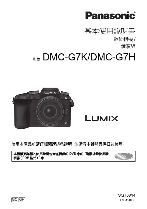
基本使用說明書數位相機/鏡頭組型號DMC-G7K/DMC-G7H使用本產品前請仔細閱讀這些說明,並保留本說明書供日後使用。
本相機更詳細的使用說明包含在提供的(PDF格式)SQT0914F0515KD0親愛的顧客,我們很高興能藉此機會感謝您購買Panasonic數位相機。
請仔細閱讀本使用說明書,並將其妥善保管以備日後參考。
請注意,您的數位相機的實際控件、元件、功能表項等看起來可能與本使用說明書的圖例中所顯示的略有不同。
請嚴格遵守版權法。
•若非個人使用,複製先期錄製的錄影帶、光碟、其他出版物或播放材料都侵犯版權法。
即使是個人使用,也嚴禁複製某些特定的材料。
安全注意事項警告:為了降低起火、電擊或產品損壞的危險,•請勿讓本機遭受雨淋、受潮、滴上或濺上水。
•請僅使用推薦的附件。
•請勿卸下蓋子。
•請勿自行維修本機。
請向有資格的維修人員請求維修。
電源插座應安裝在設備附近並應易於觸及。
∫產品標識產品位置數位相機底部電池充電器底部僅對於新加坡2SQT0914 (TCH)3(TCH) SQT0914∫關於電池•請勿將電池加熱或接觸明火。
•請勿將電池長時間放置在門窗緊閉受陽光直射的汽車內。
∫關於電池充電器•連接了AC 電源線時,電池充電器處於待機狀態。
只要電源線和電源插座相連,原電路就會始終“帶電”。
注意•如果電池更換得不正確,會有發生爆炸的危險。
請僅用製造商建議使用的類型的電池進行更換。
•廢棄電池時,請與當地機構或經銷商聯繫,詢問正確的廢棄方法。
警告電池有發生火災、爆炸和灼傷的危險。
請勿拆卸、加熱至60x C 以上或焚燒。
注意!為了降低起火、電擊或產品損壞的危險,•請勿將本機安裝或置於書櫃、壁櫥或其他密閉的空間裡。
請確保本機通風良好。
•請勿使用其他任何USB連接電纜,只使用提供的USB連接電纜或正品的Panasonic USB連接電纜(DMW-USBC1: 另購件)。
•請使用帶HDMI標誌的“High Speed HDMI micro電纜”。
IO-Link手册第三版请访问:/CN目录引言第4页第1部分:IO-Link简介第5页◆老派传感器第5页◆微型开关量传感器驱动第5页◆I O-Link:开放式低成本传感器接口第5页◆I O-Link节点第5页◆I O-Link系统第6页◆I O-Link接口在IEC 61131-9中被标准化为SDCI第6页◆物理层IO-Link标准化接口第6页◆物理层电气规范第7页◆自动化体系中的IO-Link第7页◆I O-Link:实现智能传感器第7页◆工业传感器生态系统第8页第6部分:提高系统性能第24页◆散热第24页◆测试A第24页◆测试B第24页◆测试C第24页◆热性能第24页◆分立解决方案第25页◆集成解决方案第25页◆选择TVS二极管第25页◆I O-Link保护电路第25页◆65 V(绝对最大值)如何帮助提供保护(对比40 V)第25页◆65 V绝对最大值的保护优势第25页◆小结第26页◆I O-Link信号摆率如何影响IO-Link电缆辐射?第26页引言当今的无风扇可编程逻辑控制器(PLC)和IO-Link®网关系统须消耗大量功率,具体取决于I/O配置(IO-Link、数字输入/输出、模拟输入/输出)。
随着这些PLC演变成新的工业4.0智能工厂,我们必须深谋远虑,实现更智能、更快速、更低功耗的解决方案。
这场革命的核心是一项名为“IO-Link”的新技术,能帮助实现灵活制造,从而改善工厂吞吐量,提高运营效率。
这项激动人心的新技术正使传统传感器转变为智能传感器。
ADI公司提供一系列先进的工厂自动化解决方案,并通过我们的IO-Link技术产品系列进一步改进性能,为实现工业4.0铺路架桥。
MAX22513是该产品系列的最新成员,这是一款微型双通道IO-Link收发器,集成了浪涌保护和DC-DC转换器,可减少热耗散并提高工厂车间传感器的稳定性。
为了帮助我们的客户缩短上市时间,我们与来自IO-Link联盟的软件协议栈供应商合作开发了一系列经过全面验证和测试的参考设计,本手册对此进行了详细说明。
ACV系列全线产品资料参数ACV-IR日夜两用系列热成像系统将先进的热成像能力和高清晰16倍,18倍,22倍,23倍,26倍,30倍,35倍,36倍.光学一体化摄象机及ACV高速云台精准结合在一起,制造了一个完全一体化,独一无二的日夜两用型热成像定位系统。
ACV-IR 的核心是一个非制冷微型热辐射测量计,长波红外(LWIR) 摄像机。
它可生成320 x 240 辨论率的热成像视频,每个像素大小为38 μm。
ACV-IR 系列提供杰出的低于40mK 的灵敏度。
它具有多种显示模式,包括热量呈白色,黑色,和彩色系列。
ACV-IR有三种不同的镜头配置14.25 mm, 35 mm 和50 mm 焦距为了更有效地在各种环境下应用。
产品特性:解码器集成了多种协议( RS-485Pelco D 协议和P 协议)一体化红外(IR) 摄像机防护罩变速范畴0.1-80°/ 秒360°连续水平转动垂直范畴+88°至-87°可在90 英里/ 小时风速下正常工作,能承担风速达到130 英里/ 小时在风速50英里/小时的水平预置速度为每秒80°,在90 英里/小时风速时为每秒60°符合IP66 标准—云台和防护罩变速扫描速度(0.1-60°/ 秒)译码卡支持其它品牌协议易于安装- 快速简捷的电气连接最少爱护设计,无需调整齿轮满负荷连续工作128 个可编程带标识预置位自动,和随机扫描可编程停止位可编程的手动云台限位( 水平)可编程的自动扫描限位( 水平)自动巡视模式一体化防护罩,预装配热成像摄像机遮阳罩,加热器,隔热衬垫均是标准配置AC 线性锁定NTSC/PAL电气指标输入电压AC 24V, 50/60 Hz .输入电压范畴±10%功耗最大70 V A加热器温控器操纵电气连接在安装位置有两芯电源连接头和一个地线端子;一个BNC 头和四芯接头用于RS-485 Pelco D 或P 协议;两芯接线端子用,于集电极开路输出.Aux 2 2 秒触发的电极开路输出;连接的继电器鼓舞线圈的电压不得超过32 VDC 和40 mA ;ACV-IR和继电器间的线长度必须小于100 英尺(30 m)视频同输电缆最大长度电缆型号RG59/U 750 英尺(229 m)RG6/U 1,000 英尺(305 m)RG11/U 1,500 英尺(457 m)最低线缆需求:75欧姆阻抗;全铜线芯;屏蔽层覆盖率95%机械构造参数水平转动360°连续的水平转动垂直移动+88°至-87°无阻碍变速云台速度水平0.1°至60°/ 秒变速操作,加速模式下80°/ 秒垂直每秒0.1°至40°变速操作预置位速度水平80°/ 秒垂直60°/ 秒摄像机安装一体化的摄像机安装组件热成像摄像机参数成像器非制冷微型热辐射测量计,氧化钒(VOx)辨论率320x240像素大小38 μm光谱响应7.5 至13.5 μm,长波红外(LWIR)视频输出NTSC/PAL标准化来源内部快门( 补偿) ,快门动作期间冻结视频0.7 秒成像时刻小于2 秒不带热电制冷器(TEC)串行命令兼容RS-232场景温度范畴( 取决于镜头) 150°C 标准;可选的自动增益模式扩展范畴到560°C镜头选项14.25 mm, F1.3 镜头35 mm, F1.4 镜头50 mm, F1.7 镜头目标像素(POT)以下性能值基于在正常大气环境下,安装在25 英尺(8m) 高的设备与一个单人大小的目标间的距离。
水星二代(MERCURY2)USB3.0数字相机应用说明书版本:V2.0.1发布日期:2023-07-28本手册中所提及的其它软硬件产品的商标与名称,都属于相应公司所有。
本手册的版权属于中国大恒(集团)有限公司北京图像视觉技术分公司所有。
未得到本公司的正式许可,任何组织或个人均不得以任何手段和形式对本手册内容进行复制或传播。
本手册的内容若有任何修改,恕不另行通知。
© 2023中国大恒(集团)有限公司北京图像视觉技术分公司版权所有网站:公司总机:************客户服务热线:400-999-7595销售信箱:************************支持信箱:**************************首先感谢您选用大恒图像产品,水星二代(MERCURY2)USB3.0接口数字相机是我公司最新推出的大靶面高分辨率工业数字相机,它具有高分辨率、高清晰度、低噪声等特点。
水星二代USB3.0相机包括标准版(MER2-U3(-L)系列)、Pro版(ME2P-U3系列)、Lite版(ME2L-U3(-L)系列)和Super版(ME2S-U3系列),相机采用了USB3.0标准接口,安装、使用方便。
适用于工业检测、医疗、科研、教育、安防等领域。
本手册详细介绍了水星二代USB3.0接口数字相机的应用。
1. 概述 (1)1.1. 系列概述 (1)1.2. 型号名称说明 (1)1.3. 遵循的标准 (1)1.4. 相关文档及软件下载 (1)2. 注意事项及认证声明 (2)2.1. 安全声明 (2)2.2. 使用注意事项 (2)2.3. EMI、ESD注意事项 (3)2.4. 使用环境注意事项 (3)2.5. 相机机械安装注意事项 (3)2.6. 认证声明 (3)3. 安装指南 (5)3.1. 主机端准备 (5)3.1.1. 用户软件组成 (5)3.1.2. 用户软件接口 (5)3.2. 相机供电 (6)3.2.1. MER2/ME2P/ME2L系列 (6)3.2.2. ME2S系列 (6)3.3. 相机驱动安装 (7)3.3.1. 系统要求 (7)3.3.2. 驱动安装 (7)3.4. 打开相机采集 (7)4. 性能参数 (8)4.1. 重要参数解释 (8)4.1.1. 关于光谱响应图 (8)4.2.1. MER2-041-436U3M/C(-L) (8)4.2.2. MER2-041-528U3M/C(-L) (9)4.2.3. MER2-135-150U3M/C(-L) (11)4.2.4. MER2-135-208U3M/C(-L) (12)4.2.5. MER2-160-227U3M/C(-L) (14)4.2.6. MER2-230-168U3M/C(-L) (15)4.2.7. MER2-231-41U3M/C(-L) (17)4.2.8. MER2-301-125U3M/C(-L) (18)4.2.9. MER2-302-56U3M/C(-L) (20)4.2.10. MER2-502-79U3M/C(-L) (21)4.2.11. MER2-502-79U3M POL (23)4.2.12. MER2-503-36U3M/C(-L) (24)4.2.13. MER2-503-36U3M POL (26)4.2.14. MER2-630-60U3M/C(-L/-W90) (27)4.2.15. MER2-1220-32U3M/C(-L/-W90) (29)4.2.16. MER2-2000-19U3M/C(-L/-W90) (30)4.3. ME2S-U3 系列 (32)4.3.1. ME2S-560-70U3M/C (32)4.3.2. ME2S-1260-28U3M/C (33)4.3.3. ME2S-1610-24U3M/C (35)4.3.4. ME2S-2020-19U3M/C (36)4.3.5. ME2S-2440-16U3M/C (38)4.4. ME2P-U3 系列 (39)4.4.1. ME2P-560-36U3M/C (39)4.4.2. ME2P-900-43U3M/C (41)4.4.3. ME2P-1230-23U3M/C (42)4.4.4. ME2P-1231-32U3M/C (44)4.4.5. ME2P-1840-21U3M/C (45)4.4.6. ME2P-2621-15U3M/C \ ME2P-2622-15U3M/C (47)4.4.7. ME2P-2621-15U3M NIR \ ME2P-2622-15U3M NIR (49)4.5. ME2L-U3(-L) 系列 (51)4.5.1. ME2L-161-61U3M/C(-L) (51)4.5.2. ME2L-203-76U3M/C(-L) (52)4.5.3. ME2L-204-76U3C(-L)-F02 (53)4.5.4. ME2L-505-36U3M/C(-L) (54)4.5.5. ME2L-830-22U3M/C(-L) (56)5. 机械尺寸 (58)5.1. 相机尺寸 (58)5.2. 光学接口 (61)6. 滤光片及镜头 (63)6.1. 滤光片规格参数及响应图 (63)6.2. 镜头选型参考 (64)6.2.1. HN-2M系列定焦镜头 (64)6.2.2. HN-5M 系列定焦镜头 (65)6.2.3. HN-6M 系列定焦镜头 (65)6.2.4. HN-20M 系列定焦镜头 (66)6.2.5. HN-P-6M 系列定焦镜头 (66)6.2.6. HN-P-10M 系列定焦镜头 (67)6.2.7. HN-P-20M 系列定焦镜头 (67)6.2.8. HN-P-25M 系列定焦镜头 (68)6.2.9. HN-P 系列8K~16K线扫镜头 (68)7. 电气接口 (69)7.1. LED灯状态 (69)7.1.1. MER2/ME2P/ME2L系列 (69)7.1.2. ME2S系列 (69)7.2. USB接口 (69)7.3. I/O接口 (70)7.3.1. I/O接口定义 (70)7.3.1.1. MER2/ME2P系列 (70)7.3.1.2. ME2L系列 (70)7.3.1.3. ME2S系列 (71)7.3.2. I/O电气特性 (71)7.3.2.1. Line0(光耦隔离输入)电路 (71)7.3.2.2. Line1(光耦隔离输出)电路 (74)7.3.2.3. Line2/3(双向)电路 (76)8. 功能定义 (83)8.1.1. 配置输入引脚 (83)8.1.2. 配置输出引脚 (84)8.1.3. 读取引脚状态 (89)8.2. 图像采集控制 (89)8.2.1. 开始采集/停止采集 (89)8.2.1.1. 开始采集 (89)8.2.1.2. 停止采集 (90)8.2.2. 采集模式 (91)8.2.3. 触发类型选择 (92)8.2.4. 触发模式切换 (93)8.2.5. 连续采集及其配置 (94)8.2.6. 突发采集功能 (95)8.2.7. 软触发采集及其配置 (96)8.2.8. 外触发采集及其配置 (96)8.2.9. 交叠曝光和非交叠曝光 (97)8.2.10. 设置曝光 (99)8.2.10.1. 设置曝光模式 (99)8.2.10.2. 设置Sensor曝光模式 (101)8.2.10.3. 设置曝光时间模式 (103)8.2.10.4. 设置曝光时间值 (104)8.2.11. 曝光延迟 (104)8.3. 基本属性设置 (106)8.3.1. 增益 (106)8.3.2. Sensor位深 (107)8.3.3. 像素格式 (107)8.3.4. ROI (112)8.3.5. 自动曝光和自动增益 (112)8.3.6. 测试图 (114)8.3.7. 参数组 (116)8.3.9. 时间戳 (118)8.3.10. Binning (118)8.3.11. 像素抽样 (121)8.3.12. 镜像翻转 (123)8.3.13. 数字移位 (125)8.3.14. 采集状态 (127)8.3.15. 黑电平和自动黑电平 (128)8.3.15.1. 黑电平 (128)8.3.15.2. 自动黑电平 (128)8.3.16. 取消参数范围限制 (129)8.3.17. 用户数据区 (137)8.3.18. 定时器 (138)8.3.19. 计数器 (139)8.3.20. 多帧灰度控制 (141)8.4. 图像处理 (142)8.4.1. 环境光源预设 (142)8.4.2. 自动白平衡 (144)8.4.3. 颜色转换 (145)8.4.4. Gamma (147)8.4.5. 查找表 (148)8.4.6. 锐化 (150)8.4.6.1. 锐化 (150)8.4.6.2. 带噪声抑制的锐化 (151)8.4.7. 平场校正 (152)8.4.7.1. 平场校正系数的求取和预览 (154)8.4.7.2. 系数的读取和保存 (155)8.4.7.3. 文件的读取与保存 (155)8.4.7.4. 平场校正使用注意事项 (155)8.4.8. 降噪 (156)8.5. 图像传输 (158)8.5.1. 帧率计算 (158)8.5.2. USB接口带宽 (159)8.5.3. 设备链路带宽限制 (159)8.5.4. 相机采集时间计算 (160)8.6. 事件 (166)8.6.1. 曝光结束事件 (167)8.6.2. 图像帧数据丢弃事件 (167)8.6.3. 帧存不为空事件 (168)8.6.4. 帧开始触发信号溢出事件 (168)8.6.5. 帧高速连拍开始触发信号溢出事件 (168)8.6.6. 帧开始触发信号等待事件 (168)8.6.7. 帧高速连拍开始触发信号等待事件 (168)9. 软件工具 (170)9.1. 查找表生成插件 (170)9.1.1. 界面 (170)9.1.2. 使用说明 (171)9.1.2.1. 使用场景 (171)9.1.2.2. 基准Lut选择 (171)9.1.2.3. 调整Lut (173)9.1.2.4. 保存查找表 (174)9.1.2.5. 读取Lut (174)9.1.3. 注意事项 (175)9.1.3.1. 从设备中读取 (175)9.1.3.2. Lut写入设备 (175)9.1.3.3. 目录结构 (175)9.2. 平场校正插件 (175)9.2.1. 界面 (176)9.2.2.1. 平场校正执行步骤 (177)9.2.2.2. 采集亮场图像 (177)9.2.2.3. 执行平场校正 (178)9.2.2.4. 校正数据从设备读取/写入设备 (178)9.2.2.5. 校正数据从文件加载/保存到文件 (178)9.2.3. 注意事项 (178)9.2.3.1. 平场校正实现方式 (178)9.2.3.2. 预览 (179)9.3. 帧率计算工具 (180)9.4. 静态坏点校正插件 (181)9.4.1. 界面 (181)9.4.2. 使用说明 (183)9.4.2.1. 执行静态坏点校正步骤 (183)9.4.2.2. 捕获图像 (183)9.4.2.3. 静态坏点校正 (183)9.4.2.4. 坏点数据文件使用 (184)10. 常见问题处理 (185)11. 版本说明 (187)12. 联系方式 (192)12.1. 销售联系方式 (192)12.2. 技术支持联系方式 (192)12.3. 总部及各办事处联系方式 (192)1.概述1.概述1.1.系列概述水星二代(MERCURY2)USB3.0数字相机是由大恒图像自主研发的成熟产品,性能出色、价格实惠、安装、使用方便。
光电传感器Subject to change –2018/102→Internet:/catalogue/...光电传感器SOOD,SOOE主要特性和产品范围一览产品范围一览派生型SOOD LEDSOOD 激光SOOE LED SOOE 激光→页码/Internet 漫反射式传感器,带背景抑制⏹⏹⏹⏹12,24对射式传感器⏹⏹⏹⏹18,28反射式传感器⏹⏹⏹⏹21,32反射式传感器,用于透明物体––⏹–35漫反射式传感器––⏹–38激光,对比传感器–––⏹42激光,距离传感器––⏹⏹46检测方法漫反射式传感器SOOE-DS这些传感器有时候被称为能量传感器,发射器和接收器同处一个壳体内。
发射出的光束直接被物体反射到接收器,计算反射光束的强度。
通过改变接收器(用IO-Link®、电位计或示教方法)的灵敏度可调节工作距离。
漫反射式传感器是成本效益最高的解决方案之一,安装也十分快捷。
不过,这些传感器不适用于一些应用场合,例如在强反射背景下检测轻微反光的物体。
此外,采用多种不同表面的物体(从材料、颜色或表面光洁度的角度出发)因为不同表面的反射特性不同,所以需要在不同的距离进行测量。
漫反射式传感器的优点在于强度区分。
•工作距离更长•经济性更佳•检测轻微反光的物体时更可靠-V-新产品光电传感器SOOD,SOOE 主要特性漫反射式传感器,带背景抑制工作距离并非通过能量来设定,而是通过光学三角测量。
全新且高精度的多像素技术(SOOE)有着优异的灵活性,通过IO-Link®设置。
带160x16像素的信号预处理的集成接收器是精确检测与距离测量的关键。
该接收器具备高分辨率和线性化,在检测范围上限有着独特的设定性能。
因此,物体检测几乎独立于背景中的其它物体之外,也与颜色、大小或表面光洁度无关。
这些设备仅要求有非常少量的漫反射。
带背景抑制的漫反射式传感器的优点•工作距离实际上与颜色和表面光洁度无关•还可用于闪光或反光的背景•检测距离的小差异•调节方便反射式传感器这些传感器的发射器和接收器也同处一个壳体内。
© 2007 OmniVision Technologies, Inc.VarioPixel, OmniVision, and the OmniVision logo are registered trademarks of OmniVision Technologies, Inc.Version 1.1, March 30, 2007OmniPixel2 and CameraChip are trademarks of OmniVision Technologies, Inc.These specifications are subject to change without notice.Advanced Information Preliminary DatasheetOV7725 Color CMOS VGA (640x480) C AMERA C HIP TM SensorO mniision®with OmniPixel2TM TechnologyGeneral DescriptionThe OV7725 C AMERA C HIP ™ image sensor is a low voltage CMOS device that provides the full functionality of a single-chip VGA camera and image processor in a small footprint package. The OV7725 provides full-frame,sub-sampled or windowed 8-bit/10-bit images in a wide range of formats, controlled through the Serial CameraApplications•Cellular and picture phones •Toys•PC Multimedia•Digital still camerasKey SpecificationsOV7725Color CMOS VGA OmniPixel2™C AMERA C HIP™ Sensor OFunctional DescriptionFigure2 shows the functional block diagram of the OV7725 image sensor. The OV7725 includes:•Image Sensor Array (total array of 656 x 488 pixels, with active pixels 640 x 480 in YUV mode)•Analog Signal Processor•A/D Converters•Test Pattern Generator•Digital Signal Processor (DSP)•Image Scaler•Timing Generator2Proprietary to OmniVision Technologies, Inc.Version 1.1, March 30, 2007Functional DescriptionVersion 1.1, March 30, 2007Proprietary to OmniVision Technologies, Inc.3OImage Sensor ArrayThe OV7725 sensor has an image array of 656x 488pixels for a total of 320,128 pixels, of which 640x 480pixels are active (307,200 pixels). Figure 3 shows a cross-section of the image sensor array.Figure 3 Image Sensor Arrayoperates at speeds up to 12 MHz and is fully synchronous to the pixel rate (actual conversion rate is related to the frame rate).In addition to the A/D conversion, this block also has the following functions:•Digital Black-Level Calibration (BLC)•Optional U/V channel delay •Additional A/D range controls In general, the combination of the A/D Range Multiplier and A/D Range Control sets the A/D range and maximum value to allow the user to adjust the final image brightness as a function of the individual application.Test Pattern GeneratorOL /I OH drive currentthe C AMERA C HIP sensor operation. Refer to OmniVision Technologies Serial Camera Control Bus (SCCB)Specification for detailed usage of the serial control port.4Proprietary to OmniVision Technologies, Inc.Version 1.1, March 30, 2007OV7725Color CMOS VGA OmniPixel2™ C AMERA C HIP ™ SensorOPin DescriptionTable 1Pin DescriptionPin NumberName Pin Type Function/DescriptionA1ADVDD Power ADC power supplyA2RSTB Input System reset input, active lowA3VREFH Reference Reference voltage - connect to ground using a 0.1 µF capacitor A4FSIN Input Frame synchronize input A5SCL Input SCCB serial interface clock input A6D0a a. D[9:0] for 10-bit Raw RGB data (D[9] MSB, D[0] LSB)Output Data output bit[0]B1ADGND Power ADC groundB2VREFN Reference Reference voltage - connect to ground using a 0.1 µF capacitor B3AVDD Power Analog power supply B4AGND Power Analog groundB5SDA I/O SCCB serial interface data I/O B6HREF Output HREF outputC1PWDN Input (0)b b. Input (0) represents an internal pull-down resistor.Power Down Mode Selection0:Normal mode1:Power down mode C6VSYNC Output Vertical sync output D1D5Output Data output bit[5]D6D4Output Data output bit[4]E1D7Output Data output bit[7]E2D1Output Data output bit[1]E3DVDD Power Power supply (+1.8 VDC) for digital logic core E4PCLK Output Pixel clock outputE5DOVDD Power Digital power supply for I/O (1.7V ~ 3.3V)E6D6Output Data output bit[6]F1D9c c. D[9:2] for 8-bit YUV or RGB565/RGB555 (D[9] MSB, D[2] LSB)Output Data output bit[9]F2D3Output Data output bit[3]F3XCLK Input System clock input F4DOGND Power Digital ground F5D2Output Data output bit[2]F6D8OutputData output bit[8]Electrical CharacteristicsVersion 1.1, March 30, 2007Proprietary to OmniVision Technologies, Inc.5OElectrical CharacteristicsNOTE:Exceeding the Absolute Maximum ratings shown above invalidates all AC and DC electrical specifications and may result in permanent device damage.Table 2Operating ConditionsParameterMin Max Operating temperature -20°C +70°C Storage temperature a a.Exceeding the stresses listed may permanently damage the device. This is a stress rating only and functional operation of the sensor at these and any other condition above those indicated in this specification is not implied. Exposure to absolute maximum rating conditions for any extended period may affect reliability.-40°C+125°CTable 3 Absolute Maximum RatingsAmbient Storage Temperature-40ºC to +95ºCSupply Voltages (with respect to Ground)V DD-A4.5 V V DD-C 3 V V DD-IO4.5 VAll Input/Output Voltages (with respect to Ground)-0.3V to V DD-IO +0.5V Lead-free Temperature, Surface-mount process 245ºCTable 4DC Characteristics (-20°C < T A < 70°C)Symbol ParameterConditionMin Typ Max Unit V DD-A DC supply voltage – analog – 3.0 3.3 3.6V V DD-C DC supply voltage – digital core – 1.62 1.8 1.98V V DD-IO DC supply voltage – I/O – 2.5– 3.3V I DDA Active (operating) current See Note a a.At 25ºC, V DD-A = 3.3V, V DD-C = 1.8V, V DD-IO = 3.3VI DDA = {I DD-IO + I DD-C + I DD-A }, f CLK = 24MHz at 30 fps YUV output, no I/O loading 10 + 8bb. I DD-C = 10mA, I DD-A = 8mA, without loadingmA I DDS-SCCB Standby current See Note c c. At 25ºC, V DD-A = 3.3V, V DD-C = 1.8V, V DD-IO = 3.3VI DDS-SCCB refers to a SCCB-initiated Standby, while I DDS-PWDN refers to a PWDN pin-initiated Standby 1mA I DDS-PWDN Standby current 1020µA V IH Input voltage HIGH CMOS0.7 x V DD-IOV V IL Input voltage LOW 0.3 x V DD-IOV V OH Output voltage HIGH CMOS0.9 x V DD-IOV V OL Output voltage LOW 0.1 x V DD-IOV I OH Output current HIGH See Note dd. Standard Output Loading = 25pF, 1.2K 8mA I OL Output current LOW 15mA I L Input/Output leakageGND to V DD-IO ± 1µAOV7725Color CMOS VGA OmniPixel2™C AMERA C HIP™ Sensor OTable 5 Functional and AC Characteristics (-20°C < T A < 70°C)Symbol Parameter Min Typ Max Unit Functional CharacteristicsA/D Differential non-linearity+ 1/2LSBA/D Integral non-linearity+1LSBAGC Range30dBRed/Blue adjustment range12dB Inputs (PWDN, CLK, RESET#)f CLK Input clock frequency102448MHzt CLK Input clock period2142100ns t CLK:DC Clock duty cycle455055% t S:RESET Setting time after software/hardware reset1ms t S:REG Settling time for register change (10 frames required)300ms SCCB Timing (see Figure4)f SCL Clock frequency400KHzt LOW Clock low period 1.3µs t HIGH Clock high period600ns t AA SCL low to data out valid100900ns t BUF Bus free time before new START 1.3µs t HD:STA START condition hold time600ns t SU:STA START condition setup time600ns t HD:DAT Data in hold time0µs t SU:DAT Data in setup time100ns t SU:STO STOP condition setup time600ns t R, t F SCCB rise/fall times300ns t DH Data out hold time50ns Outputs (VSYNC, HREF, PCLK, and D[9:0] (see Figure5, Figure6, Figure7, and Figure8)t PDV PCLK[ ] to data out Valid5ns t SU D[9:0] setup time15ns t HD D[9:0] Hold time8ns t PHH PCLK[ ] to HREF[ ]05ns t PHL PCLK[ ] to HREF[ ]05nsAC Conditions: V DD: V DD-C = 1.8V, V DD-A = 3.3V, V DD-IO = 3.3V Rise/Fall Times: I/O: 5ns, MaximumSCCB: 300ns, MaximumInput Capacitance: 10pfOutput Loading: 25pF, 1.2K to 3.3Vf CLK: 24MHz6Proprietary to OmniVision Technologies, Inc.Version 1.1, March 30, 2007Timing SpecificationsVersion 1.1, March 30, 2007Proprietary to OmniVision Technologies, Inc.7OTiming SpecificationsFigure 4SCCB Timing DiagramOV7725Color CMOS VGA OmniPixel2™C AMERA C HIP™ Sensor OFigure 6 VGA Frame Timing8Proprietary to OmniVision Technologies, Inc.Version 1.1, March 30, 2007Timing SpecificationsVersion 1.1, March 30, 2007Proprietary to OmniVision Technologies, Inc.9OFigure 9 RGB 565 Output Timing DiagramFigure 10OV7725Color CMOS VGA OmniPixel2™C AMERA C HIP™ Sensor OFigure 11 RGB 444 Output Timing Diagram10Proprietary to OmniVision Technologies, Inc.Version 1.1, March 30, 2007Register Set Table6 provides a list and description of the Device Control registers contained in the OV7725. For all register Enable/Disable bits, ENABLE = 1 and DISABLE = 0. The device slave addresses are 42 for write and 43 for read.Table 6 Device Control Register List (Sheet 1 of 13)Address (Hex)RegisterNameDefault(Hex)R/W Description00GAIN00RW AGC – Gain control gain setting Bit[7:0]:AGC[7:0]•Range: [00] to [FF]01BLUE80RW AWB – Blue channel gain setting •Range: [00] to [FF]02RED80RW AWB – Red channel gain setting •Range: [00] to [FF]03GREEN00RW AWB – Green channel gain setting •Range: [00] to [FF]04RSVD XX–Reserved05BAVG00RW U/B Average LevelAutomatically updated based on chip output format06GAVG00RW Y/Gb Average LevelAutomatically updated based on chip output format07RAVG00RW V/R Average LevelAutomatically updated based on chip output format08AECH00RW Exposure Value – AEC MSBsBit[7:0]:AEC[15:8] (see register AEC for AEC[7:0]} Automatically updated based on chip output format09COM201RW Common Control 2Bit[7:5]:ReservedBit[4]:Soft sleep modeBit[3:2]:ReservedBit[1:0]:Output drive capability00:1x01:2x10:3x11:4x0A PID77R Product ID Number MSB (Read only) 0B VER21R Product ID Number LSB (Read only)0C COM310RW Common Control 3Bit[7]:Vertical flip image ON/OFF selectionBit[6]:Horizontal mirror image ON/OFF selectionBit[5]:Swap B/R output sequence in RGB output modeBit[4]:Swap Y/UV output sequence in YUV output modeBit[3]:Swap output MSB/LSBBit[2]:Tri-state option for output clock at power-down period 0:Tri-state at this period1:No tri-state at this periodBit[1]:Tri-state option for output data at power-down period 0:Tri-state at this period1:No tri-state at this periodBit[0]:Sensor color bar test pattern output enable0D COM441RW Common Control 4Bit[7:6]:PLL frequency control00:Bypass PLL01:PLL 4x10:PLL 6x11:PLL 8xBit[5:4]:AEC evaluate window00:Full window01:1/2 window10:1/4 window11:Low 2/3 window Bit[3:0]:Reserved0E COM501RW Common Control 5Bit[7]:Auto frame rate control ON/OFF selection (night mode) Bit[6]:Auto frame rate control speed selectionBit[5:4]:Auto frame rate max rate control00:No reduction of frame rate01:Max reduction to 1/2 frame rate10:Max reduction to 1/4 frame rate11:Max reduction to 1/8 frame rateBit[3:2]:Auto frame rate active point control00:Not allowed01:Add frame when AGC reaches 4x gain10:Add frame when AGC reaches 8x gain11:Add frame when AGC reaches 16x gain Bit[1]:ReservedBit[0]:AEC max step control0:AEC increase step has limit1:No limit to AEC increase step0F COM643RW Common Control 6Bit[7:1]:ReservedBit[0]:Auto window setting ON/OFF selection when format changes(Hex)Name(Hex)R/W Description10AEC40RW Exposure ValueBit[7:0]:AEC[7:0] (see register AECH for AEC[15:8])11CLKRC80RW Internal ClockBit[7]:ReservedBit[6]:Use external clock directly (no clock pre-scale available)Bit[5:0]:Internal clock pre-scalarF(internal clock) = F(input clock)/(Bit[5:0]+1)/2•Range: [0 0000] to [1 1111]12COM700RW Common Control 7Bit[7]:SCCB Register Reset0:No change1:Resets all registers to default values Bit[6]:Resolution selection0:VGA1:QVGABit[5]:BT.656 protocol ON/OFF selectionBit[4]:Sensor RAWBit[3:2]:RGB output format control00:GBR4:2:201:RGB56510:RGB55511:RGB444Bit[1:0]:Output format control00:YUV01:Processed Bayer RAW10:RGB11:Bayer RAW13COM88F RW Common Control 8Bit[7]:Enable fast AGC/AEC algorithmBit[6]:AEC - Step size limit0:Step size is limited to vertical blank1:Unlimited step sizeBit[5]:Banding filter ON/OFFBit[4]:Enable AEC below banding valueBit[3]:Fine AEC ON/OFF controlBit[2]:AGC EnableBit[1]:AWB EnableBit[0]:AEC Enable(Hex)Name(Hex)R/W Description14COM94A RW Common Control 9Bit[7]:Histogram or average based AEC/AGC selection Bit[6:4]:Automatic Gain Ceiling - maximum AGC value000:2x001:4x010:8x011:16x100:32x101Not allowed110:Not allowed111:Not allowedBit[3]:ReservedBit[2]:Drop VSYNC output of corrupt frameBit[1]:Drop HREF output of corrupt frameBit[0]:Reserved15COM1000RW Common Control 10Bit[7]:Output negative dataBit[6]:HREF changes to HSYNCBit[5]:PCLK output option0:Free running PCLK1:PCLK does not toggle during horizontal blank Bit[4]:PCLK reverseBit[3]:HREF reverseBit[2]:VSYNC option0:VSYNC changes on falling edge of PCLK1:VSYNC changes on rising edge of PCLK Bit[1]:VSYNC negativeBit[0]:Output data range selection0:Full range1:Data from [10] to [F0] (8 MSBs)16REG1600RW Register 16Bit[7]:Bit shift test pattern optionsBit[6:0]:Reserved17HSTART23 (VGA)3F (QVGA)RWHorizontal Frame (HREF column) Start 8 MSBs (2 LSBs are atHREF[5:4])18HSIZEA0 (VGA)50 (QVGA)RW Horizontal Sensor Size (2 LSBs are at HREF[1:0])19VSTRT07 (VGA)03 (QVGA)RW Vertical Frame (row) Start 8 MSBs (1 LSB is at HREF[6])1A VSIZEF0 (VGA)78 (QVGA)RW Vertical Sensor Size (1 LSB is at HREF[2])1B PSHFT40RW Data Format - Pixel Delay Select (delays timing of the D[9:0] data relative to HREF in pixel units)•Range: [00] (no delay) to [FF] (256 pixel delay which accounts for whole array)(Hex)Name(Hex)R/W Description1C MIDH7F R Manufacturer ID Byte – High(Read only = 0x7F)1D MIDL A2R Manufacturer ID Byte – Low(Read only = 0xA2)1E RSVD XX–Reserved1F LAEC00RW Fine AEC Value - defines exposure value less than one row period20COM1110RW Common Control 11Bit[7:2]:ReservedBit[1]:Single frame ON/OFF selection Bit[0]:Single frame transfer trigger21RSVD XX–Reserved22BDBase FF RW Banding Filter Minimum AEC Value23BDMStep01RW Banding Filter Maximum Step24AEW75RW AGC/AEC - Stable Operating Region (Upper Limit) 25AEB63RW AGC/AEC - Stable Operating Region (Lower Limit)26VPT D4RW AGC/AEC Fast Mode Operating RegionBit[7:4]:High nibble of upper limit of fast mode control zone Bit[3:0]:High nibble of lower limit of fast mode control zone27RSVD XX–Reserved28REG2800RW Register 28Bit[7:1]:ReservedBit[0]:Selection on the number of dummy rows, N29HOutSizeA0 (VGA)50 (QVGA)RW Horizontal Data Output Size MSBs (2 LSBs at register EXHCH[1:0])2A EXHCH00RW Dummy Pixel Insert MSBBit[7:4]: 4 MSB for dummy pixel insert in horizontal direction Bit[3]:ReservedBit[2]:Vertical data output size LSBBit[1:0]:Horizontal data output size 2 LSBs2B EXHCL00RW Dummy Pixel Insert LSB8 LSB for dummy pixel insert in horizontal direction2C VOutSizeF0 (VGA)78 (QVGA)RW Vertical Data Output Size MSBs (LSB at register EXHCH[2])2D ADVFL00RW LSB of Insert Dummy Rows in Vertical Sync (1 bit equals 1 row) 2E ADVFH00RW MSB of Insert Dummy Rows in Vertical Sync2F YAVE00RW Y/G Channel Average Value30LumHTh80RW Histogram AEC/AGC Luminance High Level Threshold31LumLTh60RW Histogram AEC/AGC Luminance Low Level Threshold (Hex)Name(Hex)R/W Description32HREF00RW Image Start and Size ControlBit[7]:Mirror image edge alignmentBit[6]:Vertical HREF window start control LSBBit[5:4]:Horizontal HREF window start control LSBsBit[3]:Data output bit shift test pattern ON/OFF control Bit[2]:Vertical sensor size LSBBit[1:0]:Horizontal sensor size 2 LSBs33DM_LNL00RW Dummy Row Low 8 Bits34DM_LNH00RW Dummy Row High 8 Bits35ADoff_B80RW AD Offset Compensation Value for B Channel36ADoff_R80RW AD Offset Compensation Value for R Channel37ADoff_Gb80RW AD Offset Compensation Value for Gb Channel38ADoff_Gr80RW AD Offset Compensation Value for Gr Channel39Off_B80RW Analog Process B Channel Offset Compensation Value 3A Off_R80RW Analog Process R Channel Offset Compensation Value 3B Off_Gb80RW Analog Process Gb Channel Offset Compensation Value 3C Off_Gr80RW Analog Process Gr Channel Offset Compensation Value3D COM1280RW Common Control 12Bit[7:6]:ReservedBit[5:0]:DC offset compensation for analog process3E COM13E2RW Common Control 13Bit[7]:BLC enableBit[6]:ADC channel BLC ON/OFF controlBit[5]:Analog processing channel BLC ON/OFF control Bit[4:3]:ReservedBit[2]:ABLC gain trigger enableBit[1:0]:Reserved3F COM141F RW Edge Enhancement AdjustmentBit[7:4]:ReservedBit[3:2]:AD offset compensation optionx0:Use R/Gr channel value for B/Gb01:Use B/Gb channel value for R/Gr11:Use B/Gb/R/Gr channel value independently Bit[1:0]:Analog processing offset compensation optionx0:Use R/Gr channel value for B/Gb01:Use B/Gb channel value for R/Gr11:Use B/Gb/R/Gr channel value independently(Hex)Name(Hex)R/W Description40COM15C0RW Common Control 15Bit[7:4]:ReservedBit[3]:AD add 128 bit offsetBit[2:0]:Reserved41COM1608RW Common Control 16Bit[7:2]:ReservedBit[1:0]:BLC target 2 LSBs42TGT_B80RW BLC Blue Channel Target Value 43TGT_R80RW BLC Red Channel Target Value 44TGT_Gb80RW BLC Gb Channel Target Value 45TGT_Gr80RW BLC Gr Channel Target Value46LC_CTR00RW Lens Correction ControlBit[7:3]:ReservedBit[2]:Lens correction control select0:R, G, and B channel compensation coefficient isset by registers LC_COEF (0x49)1:R, G, and B channel compensation coefficient isset by registers LC_COEFB (0x4B), LC_COEF(0x49), and LC_COEFR (0x4C), respectively Bit[1]:ReservedBit[0]:Lens correction enable0:Disable1:Enable47LC_XC00RW X Coordinate of Lens Correction Center Relative to Array Center Bit[7]:Sign bit0:Positive1:NegativeBit[6:0]:X coordinate of lens correction center relative to array center48LC_YC00RW Y Coordinate of Lens Correction Center Relative to Array Center Bit[7]:Sign bit0:Positive1:NegativeBit[6:0]:Y coordinate of lens correction center relative to array center49LC_COEF50RW Lens Correction CoefficientG channel compensation coefficient when LC_CTR[2] (0x46) is 1 R, G, and B channel compensation coefficient when LC_CTR[2] is 04A LC_RADI30RW Lens Correction Radius – radius of the circular section where no compensation applies4B LC_COEFB50RW Lens Correction B Channel Compensation Coefficient (effective only when LC_CTR[2] is high)(Hex)Name(Hex)R/W Description4C LC_COEFR50RW Lens Correction R Channel Compensation Coefficient (effective only when LC_CTR[2] is high)4D FixGain00RW Analog Fix Gain AmplifierBit[7:6]:Gb channel fixed gainBit[5:4]:Gr channel fixed gainBit[3:2]: B channel fixed gainBit[1:0]:R channel fixed gain4E AREF0EF RW Sensor Reference Control •Range: [00] to [FF]4F AREF110RW Sensor Reference Current ControlBit[7:4]:Sensor reference current controlBit[3]:Internal regulator ON/OFF selection Bit[2]:ReservedBit[1:0]:Analog reference control50AREF260RW Analog Reference Control •Range: [00] to [FF]51AREF300RW ADC Reference Control •Range: [00] to [FF]52AREF400RW ADC Reference Control •Range: [00] to [FF]53AREF524RW ADC Reference Control •Range: [00] to [FF]54AREF67A RW Analog Reference Control •Range: [00] to [FF]55AREF7FC RW Analog Reference Control •Range: [00] to [FF]56-5F RSVD XX–Reserved60UFix80RW U Channel Fixed Value Output 61VFix80RW V Channel Fixed Value Output 62AWBb_blk FF RW AWB Option for Advanced AWB63AWB_Ctrl0F0RW AWB Control Byte 0Bit[7]:AWB gain enableBit[6]:AWB calculate enableBit[5]:ReservedBit[4:0]:WBC threshold 2(Hex)Name(Hex)R/W Description64DSP_Ctrl11F RW DSP Control Byte 1Bit[7]:FIFO enable/disable selectionBit[6]:UV adjust function ON/OFF selection Bit[5]:SDE enableBit[4]:Color matrix ON/OFF selectionBit[3]:Interpolation ON/OFF selectionBit[2]:Gamma function ON/OFF selectionBit[1]:Black defect auto correction ON/OFF Bit[0]:White defect auto correction ON/OFF65DSP_Ctrl200RW DSP Control Byte 2Bit[7:4]:ReservedBit[3]:Vertical DCW enableBit[2]:Horizontal DCW enableBit[1]:Vertical zoom out enableBit[0]:Horizontal zoom out enable66DSP_Ctrl310RW DSP Control Byte 3Bit[7]:UV output sequence optionBit[6]:ReservedBit[5]:DSP color bar ON/OFF selectionBit[4]:ReservedBit[3]:FIFO power down ON/OFF selectionBit[2]:Scaling module power down control 1Bit[1]:Scaling module power down control 2Bit[0]:Interpolation module power down control67DSP_Ctrl400RW DSP Control Byte 4Bit[7:3]:ReservedBit[2]:AEC selection0:Before gamma1:After gamma Bit[1:0]:Output selection00:YUV or RGB01:YUV or RGB10:RAW811:RAW1068AWB_bias00RW AWB BLC Level Clip69AWBCtrl15C RW AWB Control 1Bit[7:4]:ReservedBit[3]:G gain enable0:AWB adjusts R and G gain1:AWB adjusts R, G, and B gain Bit[2]:Max color gain0:Max color gain is 2x1:Max color gain is 4xBit[1:0]:Reserved(Hex)Name(Hex)R/W Description6A AWBCtrl211RW AWB Control 26B AWBCtrl3A2RW AWB Control 3Bit[7]:AWB mode select0:Advanced AWB1:Simple AWB6C AWBCtrl401RW AWB Control 46D AWBCtrl550RW AWB Control 56E AWBCtrl680RW AWB Control 66F AWBCtrl780RW AWB Control 770AWBCtrl80F RW AWB Control 871AWBCtrl900RW AWB Control 972AWBCtrl1000RW AWB Control 1073AWBCtrl110F RW AWB Control 1174AWBCtrl120F RW AWB Control 1275AWBCtrl13FF RW AWB Control 1376AWBCtrl14FF RW AWB Control 1477AWBCtrl15FF RW AWB Control 1578AWBCtrl1610RW AWB Control 1679AWBCtrl1770RW AWB Control 177A AWBCtrl1870RW AWB Control 187B AWBCtrl19F0RW AWB R Gain Range7C AWBCtrl20F0RW AWB G Gain Range7D AWBCtrl21F0RW AWB B Gain Range7E GAM10E RW Gamma Curve 1st Segment Input End Point 0x04 Output Value 7F GAM21A RW Gamma Curve 2nd Segment Input End Point 0x08 Output Value 80GAM331RW Gamma Curve 3rd Segment Input End Point 0x10 Output Value 81GAM45A RW Gamma Curve 4th Segment Input End Point 0x20 Output Value 82GAM569RW Gamma Curve 5th Segment Input End Point 0x28 Output Value 83GAM675RW Gamma Curve 6th Segment Input End Point 0x30 Output Value 84GAM77E RW Gamma Curve 7th Segment Input End Point 0x38 Output Value 85GAM888RW Gamma Curve 8th Segment Input End Point 0x40 Output Value 86GAM98F RW Gamma Curve 9th Segment Input End Point 0x48 Output Value 87GAM1096RW Gamma Curve 10th Segment Input End Point 0x50 Output Value (Hex)Name(Hex)R/W DescriptionRegister SetVersion 1.1, March 30, 2007Proprietary to OmniVision Technologies, Inc.21O88GAM11A3RW Gamma Curve 11th Segment Input End Point 0x60 Output Value 89GAM12AF RW Gamma Curve 12th Segment Input End Point 0x70 Output Value 8A GAM13C4RW Gamma Curve 13th Segment Input End Point 0x90 Output Value 8B GAM14D7RW Gamma Curve 14th Segment Input End Point 0xB0 Output Value 8C GAM15E8RW Gamma Curve 15th Segment Input End Point 0xD0 Output Value 8D SLOP 20RW Gamma Curve Highest Segment Slope - calculated as follows:SLOP[7:0] = (0x100 - GAM15[7:0]) 4/38EDNSTh00RWDe-noise Threshold8F EDGE000RWSharpness (Edge Enhancement) Control 0Bit[7:5]:ReservedBit[4:0]:Sharpness (edge enhancement) strength control90EDGE108RWSharpness (Edge Enhancement) Control 1Bit[7:4]:ReservedBit[3:0]:Sharpness (edge enhancement) threshold detection91DNSOff 10RW Auto De-noise Threshold Control92EDGE21F RW Sharpness (Edge Enhancement) Strength Upper Limit 93EDGE301RW Sharpness (Edge Enhancement) Strength Lower Limit 94MTX12C RW Matrix Coefficient 195MTX224RW Matrix Coefficient 296MTX308RW Matrix Coefficient 397MTX414RW Matrix Coefficient 498MTX524RW Matrix Coefficient 599MTX638RWMatrix Coefficient 69A MTX_Ctrl 9E RWMatrix ControlBit[7]:Matrix double ON/OFF selection Bit[6]:ReservedBit[5]:Sign bit for MTX6Bit[4]:Sign bit for MTX5Bit[3]:Sign bit for MTX4Bit[2]:Sign bit for MTX3Bit[1]:Sign bit for MTX2Bit[0]:Sign bit for MTX19B BRIGHT 00RW Brightness Control 9C CNST 40RW Contrast Gain Gain 0x209DRSVDXX–ReservedTable 6Device Control Register List (Sheet 11 of 13)Address (Hex)Register Name Default (Hex)R/W DescriptionOV7725Color CMOS VGA OmniPixel2™C AMERA C HIP™ Sensor O9E UVADJ011RW Auto UV Adjust Control 0Bit[7:4]:Auto UV adjust offset control 4 LSBs Bit[3:0]:Auto UV adjust threshold control9F UVADJ102RW Auto UV Adjust Control 1Bit[7:3]:Auto UV adjust valueBit[2]:ReservedBit[1]:Auto UV adjust stop controlBit[0]:Auto UV adjust offset control MSBA0SCAL000RW DCW Ratio ControlBit[7:4]:ReservedBit[3:2]:Vertical down sampling select00:Bypass01:1/2 vertical down sampling10:1/4 vertical down sampling11:1/8 vertical down sampling Bit[1:0]:Horizontal down sampling select00:Bypass01:1/2 horizontal down sampling10:1/4 horizontal down sampling11:1/8 horizontal down samplingA1SCAL140RWHorizontal Zoom Out ControlA2SCAL240RWVertical Zoom Out ControlA3FIFOdlyM06RW FIFO Manual Mode Delay Control A4FIFOdlyA00RW FIFO Auto Mode Delay ControlA5RSVD XX–ReservedA6SDE00RW Special Digital Effect ControlBit[7]:ReservedBit[6]:Negative image enableBit[5]:Gray scale image enableBit[4]:V fixed value enableBit[3]:U fixed value enableBit[2]:Contrast/Brightness enableBit[1]:Saturation enableBit[0]:Hue enableA7USAT40RW U Component Saturation Gain Gain 0x40Table 6 Device Control Register List (Sheet 12 of 13)Address (Hex)RegisterNameDefault(Hex)R/W DescriptionHorizontal zoom ratio =0x40SCAL1[7:0]Vertical zoom ratio =0x40SCAL2[7:0]22Proprietary to OmniVision Technologies, Inc.Version 1.1, March 30, 2007Register SetVersion 1.1, March 30, 2007Proprietary to OmniVision Technologies, Inc.23OA8VSAT 40RW V Component Saturation Gain Gain 0x40A9HUECOS 80RW Cosine value 0x80AAHUESIN80RWSine value 0x80AB SIGN 06RWSign Bit for Hue and BrightnessBit[7:4]:ReservedBit[3]:Brightness sign bit Bit[2]:ReservedBit[1]:Sign bit for HueSin (in Cr’ equation)Bit[0]:Sign bit for HueSin (in Cb’ equation)AC DSPAuto FF RWDSP Auto Function ON/OFF ControlBit[7]:AWB auto threshold control Bit[6]:De-noise auto threshold controlBit[5]:Sharpness (edge enhancement) auto strength control Bit[4]:UV adjust auto slope controlBit[3]:Auto scaling factor control (register SCAL0 (0xA0))Bit[2]:Auto scaling factor control (registers SCAL1 (0xA1 and SCAL2 (0xA2))Bit[1:0]:ReservedNOTE: All other registers are factory-reserved. Please contact OmniVision Technologies for reference register settings.Table 6Device Control Register List (Sheet 13 of 13)Address (Hex)Register Name Default (Hex)R/W DescriptionOV7725Color CMOS VGA OmniPixel2™C AMERA C HIP™ Sensor OPackage Specifications The OV7725 uses a 28-ball Chip Scale Package 2 (CSP2). Refer to Figure12 for package information, Table7 for package dimensions and Figure13 for the array center on the chip.Figure 12OV7725-CSP2 Package SpecificationsNote:For OVT devices that are lead-free, all part marking letters are lower case. Underlining the last digit of the lot number indicatesCSP2 is used.24Proprietary to OmniVision Technologies, Inc.Version 1.1, March 30, 2007。

iPhone15系列传感器尺寸终于确认_iPhone15系列iPhone15系列传感器尺寸终于确认,1/1.3英寸,与去年同款iPhone15和iPhone15 Plus的这两个版本,传感器的像素会升级到4800万,相比前代而言有了不少提升。
而且iPhone15和iPhone15 Plus版本相比之前的1200万像素来说,这次的提升还是蛮大的。
在过去的iPhone系列产品中,标准版和Pro版本的摄像头传感器区别不是很大,甚至可能采取一样的配置,只是风格上会有比较明显的不同。
苹果手机的拍摄方面其实很出色,相比国内手机来说可能只是差一个非常好用方便的拍照滤镜,其他都好说。
看到这个参数相信大家也想起了苹果去年推出的iPhone14系列,没错,iPhone15 Pro和iPhone15 Pro Max这次用的1/1.3英寸传感器就是和iPhone14 Pro和iPhone14 Pro Max是一样的,而且像素还是4800万。
由此可见苹果真的在憋iPhone16系列的大招。
但根据苹果手机影像系统的能力,其实是否一英寸大底传感器不是那么致命,对于实际拍摄来说对画面的影响远没有想象中的大,大家还是可以放心。
苹果手机的拍照主打一个真实感,画面永远是清晰感人的。
Pro版本将配置潜望式长焦摄像头,要说长焦摄像头的话拿来拍月亮是检验实力的唯一标准,想必到时候又会有许多的月亮返图。
iPhone15系列8月将量产据外媒7月7日报道,海通国际科技研究中心的分析师Jeff Pu 日前预计,iPhone 15系列将于今年8月进入量产阶段,今年下半年产量有望达到8400万部,相比去年的iPhone 14系列增长了12%。
不过,Jeff Pu也警告称,iPhone 15 Pro Max的售价可能会高于iPhone 14 Pro Max的1099美元起步价,并且iPhone 15 Pro Max将拥有iPhone 15 Pro 机型上没有的独家功能。
黑科技加身索尼全画幅微单A7 II
佚名
【期刊名称】《中国传媒科技》
【年(卷),期】2014(0)21
【摘要】索尼微单之前的机身不带防抖功能,全靠镜头支持。
如今A7II推出五轴防抖后.也完美兼容支持OS5防抖的E卡口镜头。
【总页数】1页(P68-68)
【关键词】索尼;科技;画幅;镜头
【正文语种】中文
【中图分类】TB852.1
【相关文献】
1.全画幅新基准索尼全画幅微单^TMα7Ⅲ耀世登场 [J], 大饼;
2.索尼全画幅微单A7 RII英伦行——“早春”的绅士气息 [J], 熊道森;
3.全画幅新基准索尼全画幅微单A7M3发布 [J], ;
4.索尼:索尼黑卡TMRX10 III与索尼全画幅微单TM镜头发布 [J], ;
5.暗夜捕手索尼全画幅微单A7S夜之魅 [J], 无
因版权原因,仅展示原文概要,查看原文内容请购买。
如果单从APS-C画幅上来说就是数码单反的感光元件(如CCD,CMOS)的大小比135相机的小。
APS定位于业余消费市场,共设计了三种底片画幅(H、C、P):H型,(30.3×16.6mm),长宽比为16:9;C型就是你说的APS-C规格,是在满画幅的左右两头各挡去一端,长宽比为3:2(24.9×16.6mm),于135底片同比例,是目前用得最多的画幅;P型是满幅的上下两边各挡去一条,使画面长宽比例为3:1(30.3×10.1mm),被称为全景模式。
另外还有高端数码单反上的全画幅,全画幅数码单反的感光元件和135相机的底片尺寸一样大(36×24mm)。
现在市场上在售的数码单反基本上就是全画幅,APS-C画幅,还有奥林巴斯的4/3系统(17.3×13mm)全画幅一般来讲是针对135画幅说的135画幅就是一张普通胶卷的大小,过去称为小画幅,中画幅及120画幅,其面积远远大于135画幅!中画幅相机过去、现在、将来都是高端专业广告摄影的主力军。
135的优势在于体积相对小巧,机身功能异常强大,什么高速连拍啊、超高ISO、防尘防水、高速对焦什么的。
120的优势则是画质优异,而且是异常的优异!即便是用最惨的120对上最强135,120的画质也依旧有一定优势,比如玛米亚ZD 和佳能1Ds Mark3都是2000多万像素的,但放到100%看时ZD 的像素质量要好于1Ds Mark3,如果是宾得645D的话优势就更明显了,如果你有幸用过哈苏H3D 39那么你就会知道135画幅的机器谈不上什么画质。
数码相机按档次和画质依次可分为中画幅,单反,单电(索尼叫微单),旁轴,类单反,卡片等。
中画幅相机,高档专业机,感光元件尺寸大于全画幅。
这类都是专业用的,价格昂贵。
代表品牌有哈苏,飞思,潘泰克斯等产品型号索尼A580套机(18-55mm)佳能600D套机(18-55mm II)产品图片参考报价¥54002011.07.07437商家报价¥52002011.07.14 765商家报价用户点评4.6星16名用户点评4.1星15名用户点评主要性能索尼A580套机(18-55mm)佳能600D套机(18-55mm II)发布日期2010年08月2011年02月机身特性APS-C规格数码单反单反操作方式全手动操作全手动操作传感器类型Exmor APS HD CMOS CMOS传感器尺寸23.4×15.6mm 22.3×14.9mm有效像素数1620万1800万光学变焦3倍3倍最高分辨率4912×3264 5184×3456图像分辨率3:2L(16M):4912×3264 M(8.4M):3568×2368 S(4.0M):2448×162416:9L(14M):4912×2760 M(7.1M):3568×2000 S(3.4M):2448×1376高清摄像高清(1080)高清(1080)机身马达支持不支持传感器描述长宽比:3:2除尘功能:自动,手动,添加除尘数据最大像素数1870万影像处理器DIGIC 4镜头特点索尼A580套机(18-55mm)佳能600D套机(18-55mm II)等效35mm焦距27-82.5mm 29-88mm镜头结构7组8片(2片非球面镜片,ED色散镜片)9组14片镜头说明镜头型号:DT 18-55mm f/3.5-5.6 SAM实际焦距:18-55mm镜头型号:EF-S 18-55mm f/3.5-5.6 ISII实际焦距:f=18-55mm广角镜头是否长焦镜头否否对焦方式对焦系统:类型(TTL)相位检测系统传感器:CCD线性传感器对焦点:含3个十字形对焦点的15个对焦点感光度范围:EV-1-18(ISO100)对焦模式:自动对焦,手动对焦自动对焦方式:自动,单次,连续预测对焦控制(AF-A,AF-C)焦点锁定类型:TTL辅助影像重合,相位检测测光范围EV -0.5 - 18(23℃,ISO 100)对焦模式:单次自动对焦,人工智能伺服自动对焦,人工智能自动对焦,手动对焦(MF)对焦区域广域(15个局部区域可选,使用取景器时为11点),中央定点,局域(15个局部区域可选,使用取景器时为11点)对焦点数15区9点对焦辅助TTL闪光辅助自动对焦辅助光:由内置闪光灯发出的短方式促连续闪光对焦范围250mm-无穷远250mm-无穷远近拍距离250mm-无穷远250mm-无穷远最大光圈F3.5-F5.6 F3.5-F5.6变焦方式变焦环变焦环显示功能索尼A580套机(18-55mm)佳能600D套机(18-55mm II)显示屏尺寸3英寸3英寸像素及类型92万像素可折叠式Xtra Fine液晶屏亮度控制:自动,±2.0级视野率:约100%可调角度:上下可折叠90度104万像素液晶屏,7级亮度调节屏幕功能旋转屏,高清屏旋转屏,高清屏实时取景支持传感器:实时取景影像传感器测光:1200-区域评价测光测光范围:EV1-17(全部测光模式,F1.4镜头,ISO100)视野率:约90%功能:柱状图显示,实时图像调整(曝光补偿,白平衡,创意风格中的黄昏和黑白)实时取景MF检查:传感器:Exmor APS HD CMOS视野率:约100%放大倍率:7.5倍/15倍支持长宽比设置:3:2,4:3,16:9,1:1对焦:实时模式,面部优先实时模式(反差检测)快速模式(相差检测)手动对焦(能放大约5倍/10倍)测光模式:使用图像感应器进行评价测光测光范围:EV 0-20(23℃,使用EF 50mm f/1.4 USM镜头,ISO 100)显示网格线:两种类型取景器光学光学取景器描述取景器类型:固定式眼水平系统光学取景器视野率:约95%放大倍率:0.8倍(使用50mm镜头,无限远对焦,屈光度为-1m-1时)眼距:距目镜约15mm,屈光度为-1m-1时距目镜约15mm,屈光度为-1m-1时屈光度调节:-2.5-+1.0m类型:眼平五面镜视野率:垂直/水平方向约95%(眼点约为19mm)放大倍率:约0.85倍(-1m-1,使用50mm镜头对无限远处对焦)眼点:约19mm(自目镜透镜中央起-1m-1)内置屈光度调节:约-3.0-+1.0 m-1(dpt)对焦屏:固定式,精确磨砂反光镜:快回型景深预览菜单语言25种(含简体中文)快门性能索尼A580套机(18-55mm)佳能600D套机(18-55mm II)快门类型电子控制纵走式焦平面快门机械电子快门快门速度30-1/4000秒,B门闪光同步速度:1/160秒1/60-1/4000秒(场景智能自动模式),闪光同步速度1/200秒30-1/4000秒,B门(总快门速度范围。
3月23日,认知创“芯”音画未来——2021索尼电视春季新品发布会在上海正式开幕。
在本次发布会中,索尼画谛系列8K液晶电视Z9J ,画谛系列4K OLED电视A90J、4K OLED电视A80J ,4K液晶电视X95J、X91J 和X90J等BRAVIA XR系列电视新品均由澎湃“心脏”——XR认知芯片驱动,能以超越传统人工智能的方式,实现音画体验的双重提升。
XR认知芯片重塑视听细节索尼2021 BRAVIA XR电视震撼发布一芯改变视界很多人会认为电视面板能够决定电视机的画质,其实这种认知并不全面,优秀的面板仅仅是高画质的基础,电视的画质处理芯片才是决定电视机画质最为关键的因素。
为什么采用同一面板的不同品牌电视机会呈现不同的画质就是因为采用不同的画质处理芯片。
画质芯片对于电视机,如同大脑对于人类。
通过芯片对电视机软硬件的精准控制,电视机得以呈现出卓越的音画效果。
索尼X系列图像处理芯片从X1,到X1进阶版、X1旗舰版都是对画质不断提高的结果,新推出的XR更是搭载了“认知”功能,让电视画质处理进入了智能时代。
索尼XR芯片就是以同样的方式工作,通过分析画面中的主要聚焦点,并通过增强目标对象细节的方式,确保它能像现实世界一样,以自然的纵深感脱颖而出。
索尼此前的画质处理引擎属于人工智能的初级阶段,仅仅是将画面元素分解后与数据库中的海量数据进行简单对比并优化。
而新一代的XR芯片如同其名字“认知”一样,虽然同样是分解画面每个像素、帧,但不同在于能够学习、分析并理解这些海量数据,最大的改变在于这款芯片能运用人眼观看事物存在“聚焦点”这一原理,将画面划分为不同区域与维度,通过海量的数据库对比、判断图中人眼视线集中的“聚焦点”,并在实现整体画面优化提升的基础上,对“聚焦First Scene 第一现场点”再次进行智能的针对性优化。
简单来说,索尼前代芯片是对画质的全面优化,而索尼XR芯片是在对画质全面优化的基础上,还要模拟观看者的思维,判断画面中观看者会重点关注的区域,并对这个区域的画质再进行针对性的进一步优化。
小蚁运动相机高清拆解图集
小蚁运动相机拆解图赏详情:
作为小米新推出的一款米粉玩具,小蚁运动相机内部做工与结构几何?接下来我们通过小蚁运动相机拆机拆解揭开神秘面纱。
小蚁运动相机采用了1600万像素索尼背照式图像传感器以及Ambarella A7LS图像处理器,支持最大64GB Micro SD卡扩展,最大可实现1080p@60fps以及720p@120fps甚至是480p@240fps视频拍摄,编码为
H.264,输出格式为MP4。
小蚁运动相机机身尺寸为60.4mm x42mm X21.2mm,机身重量仅72g,便携性出色。
小蚁运动相机采用可拆卸电池设计,因此在拆机之前需要将电池抠出来,这也是小蚁运动相机拆机第一步,如图所示。
卸下电池后,接下来就可以拆卸小蚁运动相机前面板了。
小蚁运动相机采用了卡扣式固定,表面并没有固定螺丝,因此拆解上也并不难,甚至徒手都能够搞定。
拆卸下小蚁运动相机前面板后,就可以看到这款运动相机的内部结构了,内部可以看到主板固定支架、轻量化的塑料材质,镀镍风格金属漆。
正面的黄色排线上分布着6颗LED,小蚁运动相机的电量指示环就是靠它来实现。
Capture stunning 1920 x 1080 Full HD video and 3.0 megapixel images with the ultra-compact HDR-CX150, whichfeatures an "Exmor R" CMOS sensor for superior low-light performance, 16GB of embedded flash memory, and a Carl Zeiss® Vario Tessar 25x optical zoom lens to help bring you closer to the action.2 11920x1080 Full HD Recording:1920 x 1080 high definition resolution lets you record your memories inexceptional Sony® Full High Definition quality . Capable of 1080/60pplayback via HDMI™ and compatible HDTV providing stunning clarity and incredibly detailed playback of your memories.2 43 megapixel still image capture:3 megapixel still image capture lets you take high resolution digital photos.16GB embedded Flash memory The built-in 16GB embedded Flash memory can record and store up to 6 hours of high definition video footage (HD LP mode), or up to4 hours of standard definition footage (SD HQ mode).1 1 1/4" back-illuminated "Exmor R" CMOS sensorA 1/4” "Exmor R" CMOS image sensor delivers bright, vivid, spectacularly detailed video footage, as well as 3 megapixel still images.Back-illuminated "Exmor R" CMOS sensorExperience stunning low-light sensitivity with improved image clarity anddrastically reduced grain with the back-illuminated "Exmor R" sensor. Designed for compact cameras and camcorders, the "Exmor R" sensor relocates the photo diodes above the support circuitry,maximizing the light gathering area per pixel so you can shoot with better results in lower lighting conditions.2x faster Quick AF With the new and improved autofocus (AF) system, Quick AF, the focusing speed is twice as fast compared to previous models. Whether in bright daylight or in dimly lit environment, Quick AF ensures fast, accurate, and consistent focus lock, enabling users to shoot in a wide range of scenes without missing any important moment. Especially when shooting night scenes where conventional AF might struggle to focus, thanks to the much improved AF algorithm in Quick AF, users can nowcapture crisp images, fast.1080/60p playback via HDMI™ andcompatible HDTV 1080/60p playback via HDMI™ andcompatible HDTV providing stunningclarity and incredibly detailedplayback of your memories.44 Carl Zeiss™ Vario-Tessar lens:The professional-quality Carl Zeiss®Vario-Tessar® lens designedspecifically for compact camcorders. Precision ground optics help maintain the sharpness and contrast of larger lenses, and SteadyShot™ image stabilization helps reduce blur caused by camera shake.Face Detection technology w/ Face Priority With Face Priority, your camcorder optimizes focus, color, exposure, and Smile Shutter™ technology for the faceyou prioritize. Just touch the preferredface on the LCD display and thecamcorder will assign it priority, even ifit leaves and returns to the frame.Smile Shutter™ technology for still anddual capture:Smile Shutter™ technology lets the camcorder automatically take still photos when your subject smiles, even while shooting high definition video. You can also set the sensitivity and choose child, adult, or auto priority.Direct Copy to external HDD w/o PC Store your memories in a whole new way with the ability to copy videos from your camcorder directly to an external hard disk drive (sold separately), all without a computer. Your camcorder can also 13 13 ADDITIONAL FEATURES Highlight Playback with Highlight Scenario playback 2.7” Clear Photo™ LCD (230 K) display 3Intelligent Auto (9 iAuto modes)SteadyShot® image stabilization with Active Mode:Up to 24Mbps AVCHD video2 25X Optical / 300X Digital Zoom:Power On by opening LCD display:Personalized Menu System Dolby® Digital stereo recording with Built-in Zoom Mic:Dual Record with still image capture:Face Index function:Film Roll Index:Built-in Intelligent Flash:x.v. Color™ technology for superior color:BIONZ™ Image Processor: Dynamic Range Optimizer:Hybrid Recording to 16GB internalmemory or Memory Stick Duo™ media: 1 One Touch Disc Burn:Record and zoom controls on LCD:BRAVIA® Sync™ technology: HDMI™ connection output: USB 2.0 interface:Sony Electronics Inc. • 16530 Via Esprillo • S an Diego, CA 92127 • 1.800.222.7669 • w Last Updated: 06/23/2010Please visit the Dealer Source for more informationat /dealersourceSpecificationsConvenience FeaturesMultiple Language Display: YesManual / Auto Lens Cover: Manual Quick On: Power On by LCDS/S & Zoom button on LCD: Yes Fader Effect(s): Black, WhiteOptics/LensAperture: F1.8-2.6Filter Diameter: 30mmFocal Distance: 2.5 - 62.5mmProgressive Shutter Mode: Yes (Still Image) Optical Zoom: 25xDigital Zoom: 300xResolution: 3 megapixel stillLens Type: Carl Zeiss® Vario-Tessar®Focal Length (35mm equivalent): 37 - 1075mm (16:9), 45 - 1325mm (4:3)PowerBattery Type: InfoLITHIUM® with AccuPower™ Meter System (NP-FV50)Power Requirements: 7.2V (battery pack); 8.4V (AC Adaptor)Power Consumption (in Operation): 3.0WSoftwareOperating System Compatibility: "Windows XP SP3 * /Windows Vista SP2 ** /Windows7* 64-bit editions and Starter (Edition) are notsupported.The Windows Image Mastering API(IMAPI)Ver.2.0 or later is required to use the function for creating discs.** Starter (Edition) are not supported. Standard installation is required.Operation is not assured if the above OS has been upgraded or in a multi-boot environment. "Supplied Software: PMB Ver.5.0 - Windows XP Service Pack3 (SP3)(32bit),Windows Vista Service Pack2 (SP2)(32bit), Windows 7. Not supported by Mac OS.LCD DisplayLCD Type: 2.7” Clear Photo™ LCD (230 K) displayAdvanced FeaturesFace Detection: Yes - video and stillImage Stabilization: SteadyShot® image stabilization w/ Active mode x.v.Color™: YesSmile Shutter™ technology: YesIntelligent Auto: Yes (Auto, Landscape, Backlight, Twilight, Spotlight, Low light, Macro, Portrait, Baby, Tripod)RecordingVideo Actual (Pixel): 1350K Pixels (16:9) 1010K Pixels (4:3)Dual Record: 2.7 megapixel (16:9)Photo Capture from Movie: Yes Audio Format: Dolby® Digital 2chMicrophone/Speaker: Built-in Zoom MicrophoneStill Image Max Effective Resolution: 3 megapixel Still Image Mode: JPEGVideo Format: HD: MPEG4 AVC/H.264; SD: MPEG2Video Signal: HD: 1920 x 1080/60i; SD: NTSC color, EIA standardsMedia Type: 16GB Non-Removeable Flash Memory; Memory Stick PRO Duo™ MARK2 Media andSD/SDHC/SDXC (Class 4) media (Sold Separately) Recording and Playback Times: 16GB Flash:High Definition: FX = up to 85 min., FH = up to 115 min., HQ = up to 230 min., LP = up to 395 min. Standard Definition: HQ = up to 235 min.Exposure SystemMinimum Illumination: 3 lux(Auto Slow Shutter ON, 1/30 Shutter Speed )Exposure Settings: Yes (Touch Panel)D-Range Optimizer: YesScene Mode(s): Auto, Twilight, Candle, Sunrise & Sunset, Fireworks, Landscape, Portrait, Spotlight, Beach, Snow White Balance Mode: Auto, Outdoor, Indoor, One Push (via Touch panel)InterfaceDirect Copy: YesBRAVIA® Sync™: YesSD Output: Included (via A/V Remote Terminal) ; Video / S Video / Audio / Component Out / Remote USB Port(s): Hi-speed (2.0 compliant) HD Output: HDMI (mini) PhotoTV HD: YesImaging SensorProcessor: BIONZ™ image processorEffective Picture Resolution: 1180K Pixels (16:9) 1570K Pixels (4:3)Imaging Sensor: 1/4" back-illuminated "Exmor R" CMOS sensorFocus ControlFocus System: Full range Auto / Manual (Touch Panel)Service and Warranty InformationLimited Warranty Term: Limited Warranty --- 1 Year Parts; 90 Days LaborDimensionsWeight: w/o battery: 7oz (210g), w battery: 9oz (260g) Measurements: 2 x 2 1/4 x 4 1/4 inch (50 x 56 x 114mm)Supplied AccessoriesAC adaptor (AC-L200)Rechargable Battery Pack (NP-FV50) Component A/V CableA/V Connecting CableLithium Battery (CR2025)Application Software / USB Driver / (CD-ROM) USB CableOptional AccessoriesRechargeable InfoLITHIUM Batteries (NP-FV50/FV70/FV100) AC Adaptor/Charger for H series batteries (AC-VQV10) Travel Charger (BC-TRV)HDMI Cable (mini) (VMC-30MHD) UPC Code: 027*********1. 16GB equals 16 billion bytes. A portion of the total storage is used for system management and/or application files. The capacity that a user can use is approximately 15.5GB.2.This camcorder captures high definition footage in the AVCHD format. High Definition AVCHD discs can be created using standard DVD media, the supplied software and a compatible PC. DVD mediacontaining AVCHD footage may be played on a compatible Blu-ray Disc™ player/recorder, PC with supplied software or PLAYSTATION®3 devices. DVD media containing AVCHD footage should not be used with standard DVD based players, as the DVD player may fail to eject the media and may erase its contents without warning. 3. Viewable area measured diagonally.4. HD viewing requires compatible HDTV and HDMI™ cable, both sold separately.5. Requires BRAVIA Sync feature in each product, including a compatible BRAVIA® HDTV. Please refer to owner’s manual to determine compatibility.7. By using Picture Motion Browser software, supplied with certain Sony cameras and camcorders*, a PC and a broadband Internetconnection, your photos can be shown on an online map service. The online map service is currently provided courtesy of Google, and is subject to change or termination without notice.9. Requires Microsoft Windows XP SP3/ Windows Vista SP2/Windows 7. Picture Motion Browser software not supported by Mac OS.10. Smooth Slow Record captures 3 seconds of video which play back over 12 seconds.12. One Touch Disc Burn feature requires DVDirect burner or compatible PC with supplied PBM software (sold separately).13. Requires USB 2.0 connection via VMC-UAM1 cable (sold separately), AC power for camcorder, and hard drive formatted in FAT-32. Connection via USB-hub not supported. External HHD/USB media should be less than 2TB(Terabytes).© 2009 Sony Electronics Inc. All rights reserved. Reproduction in whole or in part without written permission is prohibited. Sony, AccuPower, BIONZ, BRAVIA, Clear Photo LCD Plus, ClearVid, Exmor R, Handycam, InfoLITHIUM, Optical SteadyShot, Smile Shutter, x.v. Color, Memory Stick Duo,Memory Stick PRO Duo, Memory Stick and the Memory Stick logo are trademarks or registered trademarks of Sony Corporation. PlayStation is a registered trademark of Sony Computer Entertainment. Microsoft, Windows, and Windows Vista are registered trademarks of MicrosoftCorporation in the United States and/or other countries. Blu-ray Disc and it’s logo are trademarks. Dolby is a registered trademark of Dolby Laboratories. HDMI is a trademark of HDMI Licensing LLC. All other trademarks are trademarks of their respective owners.*Logo mentions need to be included if logo shown or listed in copy。
SERVICE MANUALDIGITAL MUSIC PLAYERSPECIFICATIONSNW-S603/S605/S703F/S705F/S706FPhoto: NW-S603Ver. 1.4 2007.04– Continued on next page –9-887-449-052007D05-1© 2007.04Sony CorporationConnect Business DivisionPublished by Sony Techno Create CorporationUS ModelNW-S703F/S705FCanadian ModelNW-S603/S705F/S706FAEP Model UK Model NW-S603/S605/S703F/S705F/S706FE ModelNW-S603/S703F/S705F/S706FAustralian Model T ourist ModelNW-S703F/S705F/S706FChinese ModelNW-S603/S605/S705F• SonicStage and the SonicStage logo are trademarks or registered trademarks of Sony Corporation.• OpenMG, ATRAC, ATRAC3, ATRAC3plus, ATRAC Advanced Lossless and their logos are trademarks of Sony Corporation.• “WALKMAN” and “WALKMAN” logo are registered trademarks of Sony Corporation.• Microsoft, Windows, Windows NT and Windows Media are trademarks or registered trademarks of Microsoft Corporation in the United States and/or other countries.• Adobe and Adobe Reader are trademarks or registered trademarks of Adobe Systems Incorporated in the United States and/or other countries.• MPEG Layer-3 audio coding technology and patents licensed from Fraunhofer IIS and Thomason.• IBM and PC/AT are registered trademarks of International Business Machines Corporation.• Macintosh is a trademark of Apple Computer, Inc.• Pentium is a trademark or a registered trademark of Intel Corporation.• CD and music-related data from Gracenote, Inc., copyright © 2000-2006 Gracenote. Gracenote Software, copyright © 2000-2006 Gracenote. This product and servicemay practice one or more of the following U.S. Patents: #5,987,525; #6,061,680; #6,154,773, #6,161,132, #6,230,192, #6,230,207, #6,240,459, #6,330,593, and other patents issued or pending. Some services supplied under license from Open Globe, Inc. for U.S. Patent: #6,304,523. Gracenote and CDDB are registed trademarks of Gracenote. The Gracenote logo and logotype, and the “Powered by Gracenote” logo are trademarks of Gracenote.• All other trademarks and registered trademarks are trademarks or registered trademarks of their respective holders. In this manual, TM and ® marks are not specified.Audio compression technology– MPEG-1 Audio Layer-3 (MP3)– Windows Media Audio (WMA)*– Adaptive Transform Acoustic Coding (ATRAC) – Advanced Audio Coding (AAC)* – Linear-PCM (PCM)* Copyright protected WMA/AAC files cannot be played back.Maximum recordable number of songs and time (Approx.)*Except ATRAC Advanced Lossless. Compression rate of ATRAC Advanced Lossless varies depending on songs.For example, one CD (containing 15 4-minute songs) is approximately 200 to 500 MB.The approximate times are based on a transferred or recorded 4-minute ATRAC *, MP3 or Linear-PCM format song. Other playable audio file formats may be different from ATRAC or MP3 format.160 kbps 82054 hr. 40 min.192 kbps 68545 hr. 40 min.256 kbps 51534 hr. 20 min.320 kbps 41027 hr. 20 min.352 kbps 37525 hr. 00 min.1411 kbps (Linear-PCM)946 hr. 10 min.Capacity (User available capacity)*NW-S603/S703F: 1 GB (Approx. 968 MB = 1,015,726,080 bytes)NW-S605/S705F: 2 GB (Approx. 1.89 GB = 2,035,974,144 bytes)NW-S706F: 4 GB (3.79 GB = 4,075,716,608 bytes)*Available storage capacity of the player may vary.A portion of the memory is used for data management functions.Bit rate Songs Time Sampling frequency *MP3: 32, 44.1, 48 kHz WMA: 44.1 kHz ATRAC: 44.1 kHzAAC: 11.025, 12, 16, 22.05, 24, 32, 44.1, 48 kHz Linear-PCM: 44.1 kHz*Sampling frequency may not correspond to all encoders.Supported bit ratesMP3: 32 to 320 kbps variable bit rate-compliant WMA: 32 to 192 kbps variable bit rate-compliantATRAC: 48/64/66 (ATRAC3)*/96/105 (ATRAC3)*/128/132 (ATRAC3)/160/192/256/320/352 kbps*ATRAC Advanced Lossless *: 64/128/132 (ATRAC3 base layer)/ 256/352 kbps*AAC: 16 to 320 kbps variable bit rate-compliant **Nonstandard bit rates or non-guaranteed bit rates are included depending on the sampling frequency.The bit rate description of ATRAC Advanced Lossless shows the bit rate for the contents which enables fast transfer to ATRAC compatible devices or media.CD recording cannot be done using the SonicStage software in ATRAC3 at 66/105 kbps.Linear-PCM: 1411 kbps2NW-S603/S605/S703F/S705F/S706FTABLE OF CONTENTS1.SERVICING NOTES ...............................................32.GENERAL ...................................................................53.DISASSEMBL Y3-1.Disassembly Flow ...........................................................63-2.Cover (Rear) Assy ...........................................................73-3.Window ...........................................................................73-4.Button (3D) Assy.............................................................83-5.Holder (Rear)...................................................................83-6.MAIN Board Scetion.......................................................93-7.Lithium Ion Battery, MAIN Board..................................93-8.OLED Sub Assy ..............................................................103-9.SWITCH Board...............................................................103-10.Knob (Jog).......................................................................113-11.Headphone Assy..............................................................124.TEST MODE ..............................................................135.DIAGRAMS5-1.Block Diagram ................................................................145-2.Printed Wiring Board – MAIN Board (Side A) –............165-3.Printed Wiring Board – MAIN Board (Side B) –............175-4.Schematic Diagram – MAIN Board (1/7) –....................185-5.Schematic Diagram – MAIN Board (2/7) –....................195-6.Schematic Diagram – MAIN Board (3/7) –....................205-7.Schematic Diagram – MAIN Board (4/7) –....................215-8.Schematic Diagram – MAIN Board (5/7) –....................225-9.Schematic Diagram – MAIN Board (6/7) –....................235-10.Schematic Diagram – MAIN Board (7/7) –....................245-11.Printed Wiring Board – SUB Board –.............................255-12.Schematic Diagram – SUB Board –................................255-13.Printed Wiring Board – SWITCH Board (Side A) –.......265-14.Printed Wiring Board – SWITCH Board (Side B) –.......275-15.Schematic Diagram – SWITCH Board –........................286.EXPLODED VIEWS6-1.Cover (Rear) Assy Section (NW-S603/S605).................386-2.Cover (Rear) Assy Section(NW-S703F/S705F/S706F).............................................396-3.Window Section ..............................................................406-4.MAIN Board Section.......................................................416-5.SWITCH Board Section..................................................426-6.Frame Scetion..................................................................437.ELECTRICAL PARTS LIST (44)Notes on chip component replacement •Never reuse a disconnected chip component.•Notice that the minus side of a tantalum capacitor may be damaged by heat.Flexible Circuit Board Repairing•Keep the temperature of the soldering iron around 270 ˚C during repairing.•Do not touch the soldering iron on the same conductor of the circuit board (within 3 times).•Be careful not to apply force on the conductor when soldering or unsoldering.Frequency response20 to 20,000 Hz (single signal measurement)FM Frequency range (NW-S703F/S705F/S706F only)87.5 to 108.0 MHzIF (FM)375 kHzAntennaHeadphone cord antennaInterfaceHeadphone: Stereo miniWM-PORT (multiple connecting terminal): 22 pin Hi-Speed USB (USB 2.0 compliant)Operating temperature 5°C to 35°C (67°F to 95°F)Power sourceBuilt-in rechargeable lithium-ion batteryUSB power (from a computer through supplied USB cable)Battery life (continuous playback)**This is when the power save setting is “Save ON Super,” and Equalizer, VPT ,Clear Stereo , or Dynamic NormalizerDimension (w/h/d)(w/h/d, projecting parts not included)87.2 × 27.4 × 14.9 mm (3.4 × 0.9 × 0.6 inches)MassSupplide AccessoriesApprox. 47 g (Approx. 2 oz)Please check the accessories in the package.Headphones (1)Headphone extension cord (1)Earbuds (Size S, L) (1)USB cable (1)Attachment (1)Use when connecting the player to the optional cradle (BCR-NWU3)*,etc.CD-ROM * (1)Quick Start Guide (1)- SonicStage software- Operation Guide (PDF file)*Available soon.Depending on the country/region in which you have purchased the player, some optional accessories may not be available.*Do not attempt to play this CD-ROM in an audio CD player.Design and specifications are subject to change without and foreign patents licensed from Dolby Laboratories.CAUTIONDanger of explosion if battery is incorrectly replaced.Replace only with the same or equivalent type.3NW-S603/S605/S703F/S705F/S706FNOTE THE IC201, IC2701, IC3005 AND IC3007 ON THE MAIN BOARD REPLACINGReplacement of IC201, IC2701, IC3005 and IC3007 on the MAIN board used in this set requires a special toolNOTE THE IC101, IC401 AND IC3001 ON THE MAIN BOARD REPLACINGWhen IC101, IC401 and IC3001 on the MAIN board is damaged,exchange the new MAIN board for the MAIN board which IC damagedNOTE THE IC1301 ON THE SUB BOARD REPLACINGWhen IC1301 on the SUB board is damaged, exchange the new SUB board for the SUB board (included in MAIN board) which IC damagedSECTION 1SERVICING NOTESNOTE THE MAIN BOARD REPLACINGWhen the MAIN board is replaced, format it according to the following.UNLEADED SOLDERBoards requiring use of unleaded solder are printed with the lead-free mark (LF) indicating the solder contains no lead.(Caution:Some printed circuit boards may not come printed withthe lead free mark due to their particular size): LEAD FREE MARKUnleaded solder has the following characteristics.•Unleaded solder melts at a temperature about 40 ˚C higher than ordinary solder.Ordinary soldering irons can be used but the iron tip has to be applied to the solder joint for a slightly longer time.Soldering irons using a temperature regulator should be set to about 350 ˚C.Caution:The printed pattern (copper foil) may peel away ifthe heated tip is applied for too long, so be careful!•Strong viscosityUnleaded solder is more viscou-s (sticky, less prone to flow)than ordinary solder so use caution not to let solder bridges occur such as on IC pins, etc.•Usable with ordinary solderIt is best to use only unleaded solder but unleaded solder may also be added to ordinary solder.Minimum System Requirements (for the player)• ComputerIBM PC/AT orcompatible computer preinstalled with the following Windows operating systems:– Windows 2000 Professional (Service Pack 3 or later)– Windows XP Home Edition – Windows XP Professional– Windows XP Media Center Edition– Windows XP Media Center Edition 2004– Windows XP Media Center Edition 2005Not supported by OSs other than above. • CPU: Pentium III 450 MHz orhigher • RAM: 128MB or more• Hard Disk drive: 200MB or more of available space (1.5GB or more is recommended)More space may be required, depending on the version of the operating system. Additional space is required for storing music data. • Display:– Screen Resolution: 800 × 600 pixels (or higher) (recommended 1,024 × 768 or higher)– Colors: High Color (16bit) (or higher) (SonicStage may not operate properly at color settings at or below 256 colors.)• CD-ROM drive (supporting Digital Music CD play back capabilities using WDM) To create original CDs or to back up audio CDs, a CD-R/RW drive is required. • Sound board• USB port (Hi-Speed USB is recommended)• Internet Explorer 5.5 or later needs to be installed.• Internet connection is required to use the CD Data Base (CDDB) or Electronic Music Distribution (EMD).We do not guarantee operation for all computers even if they meet the above System Requirements.Not supported by the following environments:– Personally constructed computers or operating systems– An environment that is an upgrade of the original manufacturer-installed operating system – Multi-boot environment – Multi-monitor environment – MacintoshFormatting Memory (Format)If the memory is formatted, all music data, other stored data and registered jacket pictures will be erased. Be sure to verify the data stored in memory prior to formatting and export any necessary data to SonicStage or the hard disk of your computer.Y ou can format the built-in flash memory of the player.This function is only available in the stop mode.To cancel formattingSelect “Cancel” in step and press the button.To return to the previous menu Press the DISPLAY/HOME button.Do not format the built-in flash memory of the player using Windows Explorer.NoteNW-S603/S605/S703F/S705F/S706F COLOR VARIATIONModel DestinationCOLORBLACK BLUE GOLD PINK VIOLETCND (Clamshell)z z zCE7z z zNW-S603CEW z zKR zCH zCE7z z zNW-S605CEW zCH zUS (Clamshell)z zCE7z z z zCEV z z NW-S703F CEW z z E, AUS, JE z zMX z zKR z zUS (Clamshell)zCND (Clamshell)z zCE7z z z zNW-S705F CEV zE, AUS, JE z z MX z z KR z z CH zCND (Clamshell)zCE7z zCEV zNW-S706FE, AUS, JE zMX zKR z•AbbreviationAUS: Australian modelCE7: AEP and UK modelsCEV: East European modelCEW: French modelCH: Chinese modelJE: Tourist modelKR: Korean modelMX: Mexican modelVer. 1.245NW-S603/S605/S703F/S705F/S706FSECTION 2GENERALThis section is extracted frominstruction manual.WM-PORTConnect to the supplied USB cable, accessories for WM-PORT such as optional accessories for recording with the player, or peripheral device.Display* buttonStarts song playback. When starting playback, appears in the display,and if thebutton is pressed again, appears and playback stops.When a menu appears on the display, of the menu.use this button to confirm the item HintWhen you stop song playback or FMThere is no power button on the player.Sleep status.power.VOL +**DISPLAY/HOME buttonWhen you press this button while the player is in the play or stop mode, you can change the display.Press and hold this button to display the HOME screen.While the menu appears, when this button is pressed again, the previous screen returns and when pressing and holding, the screen returns to the HOME screen.Shuttle switchBy rotating the shuttle switch, you can select a menu item, skip to thebeginning of the song, or fast-forward /fast-rewind.You can also set to the FOLDER mode or normal mode by sliding the shuttleswitch.Parts and ControlsTo operate the player with the shuttle switchHOLD switchY ou can protect the player against accidental operation by using the HOLD switch when carrying it.By sliding the HOLD switch to the HOLD position, all operation buttons are disabled. If you press buttons or rotate the shuttle switch while the HOLD function isactivated, “HOLD” appears in the display. If you slide the HOLD switch to the opposite position, the HOLD function is released.Press and hold this button to change the sound quality setting.Headphone jackFor connecting the headphones.Connect until it clicks into place.If connecting the headphones improperly, it may not sound right.For NW-S703F/S705F/S706F users Connect the headphone plugsecurely following to the plug shape for the headphones, and to theshape for the headphone extension cord.About the Noise Canceling function (NW-S703F/S705F/S706F only)available only when using the The Noise Canceling function is supplied headphones.Noise Canceling does not work with models without the Noise Canceling function (NW-S603/S605), even if the supplied headphones are used.When selecting Jacket Mode ON (Default setting)DisplayJacket picture display Displays the jacket picture of an album after you register the jacket and transfer songs from SonicStage. Y ou can set the jacket picture to not display.Icon indicationFor the normal mode, displays the first mine, and displays on or according to the song order setting on the second line.For the FOLDER mode, displays an icon of the category set in the song order on the first line, and displays or on the second line.When selecting the FOLDER mode during playback of a playlist, Text/graphic information display Displays album title, artist name, song title, current date and time, messages and menu.To change the display mode, press the DISPLAY/HOME button.Switch the display to the Power Save mode when you do not operate the player for a while.When selecting Jacket Mode OFFPlaying status indicationDisplays the current play mode (:playback, :stop,(): fast-rewinds (fast-forwards),():skips to the beginning of the current (or next) song).Lapse time indication Displays the elapsed time.Play mode indication (PLAY MODE)Displays the current play mode icon. If the play mode is set to “Normal,” no icon appears.Sound quality setting indication Displays the current sound quality icon. If the sound quality is not set, no icon appears.Noise Canceling indication (NW-S703F/S705F/S706F only)Displays when the Noise Canceling function is set.Remaining battery indication Displays the remaining battery power.HintFor information on the FM tuner (NW-S703F/S705F/S706F only) display, see “Enjoy Listening to FM Radio”.NW-S603/S605/S703F/S705F/S706F6•This set can be disassembled in the order shown below.3-1.DISASSEMBL Y FLOWNote 1:The process described in can be performed in any order.Note 2:Without completing the process described in , the next process can not be performed.SECTION 3DISASSEMBLYNW-S603/S605/S703F/S705F/S706F7Note: Follow the disassembly procedure in the numerical order given.3-2.COVER (REAR) ASSY24Please replace to brand-new part ones knob (hold) is removed.Note2:On installation of knob (hold),adjust the position of switch (S505)and knob (hold).3-3.WINDOWNote1:Please work noting that the window is damaged.Please replace to brand-new part ones adhesive sheet (window) is removed.1Insert a bar into the position shown in the figure,and push it to remove the window, not giving an excessive force.NW-S603/S605/S703F/S705F/S706F83-4.BUTTON (3D) ASSY3-5.HOLDER (REAR)311button (sound)24Ver. 1.1NW-S603/S605/S703F/S705F/S706F93-6.MAIN BOARD SECTION3-7.LITHIUM ION BATTERY, MAIN BOARD5SUB board8Note:Because adhesive sheet (SUB PWB)is attached, remove the SUB board,not giving an excessive force.Note:08main PWB sheet9Ver. 1.1NW-S603/S605/S703F/S705F/S706F103-8.OLED SUB ASSY3-9.SWITCH BOARD1(B1.4)(B1.4)3sheet6(NW-S703F/S705F/S706F only)Ver. 1.1NW-S603/S605/S703F/S705F/S706F113-10.KNOB (JOG)1Push the knob (JOG)2NW-S603/S605/S703F/S705F/S706F123-11.HEADPHONE ASSY4829NW-S603/S605/S703F/S705F/S706F•IC Block Diagrams – MAIN Board –IC201S71PL032J08BFW0B0A7DQ6NC A16XCE1F XOE DQ9DQ3DQ4DQ13DQ15NC DQ1VSSA0XLB XWP/ACCXWE A8A11A3A6XUB XRSTF CE2S A19A12A15D Q 12D Q 7V S S D Q 8D Q 2D Q 11N C D Q 5D Q 14V C C S V C C FD Q 10D Q 0X CE 1SA A A 1R Y /XB A 2A A 1N A A A 1A 1A 1N IC401MM3306-XRREVOSW2VOSW1OSC CPRTSS_1TSS_2SW1VIN GND SHDN RDY SW2V I N S W 2V I N _R E G N C N CV O _R E GV I N S W 1F B V O U TG N D G N D V O U T F B30NW-S603/S605/S703F/S705F/S706FIC2701TK63727BCB-GIC601MAX8670AUSB_SUS IU4PG_IO LX_IO IN_IO OUT_CORE IN_CORE LX_CORE PG_AOREENOUT_IOUSB_H/L USB_IN1USB_IN2SYS1SYS2BAT1BAT2XCHG_STAT XCHG_ENI U 6I N _U S B 3.3O U T _U S B 3.3V LI U 7I U 8I U 9U S B _P O K S H E E L D X C H G _F L T I U 5T H C H G _I S E C G N I U I N _A O U T _A I U B I U GND VCONTVINVOUTNW-S603/S605/S703F/S705F/S706FIC2702SDFMM1N23GB2TVCC X2X1CL LAANT GND RSSO G N D S T O D -G N DA U D I O R I G H A U D I O L E FD IC3001NLAS4717EPFCT1GNC2IN1NC1VCCIN2COM2N O 1C O M 1G N N OIC3004MAX5489ETEVDD HB WB LB N.C.SCLK DINCS N .C .H AW A L A N .C N .C N .C G N IC3005, 3007TK63726BCB-GGND VCONTVINVOUTNW-S603/S605/S703F/S705F/S706F– SWITCH Board –X801RX-4574LCN.C.N.C./AIRQ /TIRQ FOUTFCON CLK CE1VDD GNDCE0DATANW-S603/S605/S703F/S705F/S706F•IC Pin Function DescriptionMAIN BOARD IC101 CXD5090B1-003GG (CPU)Pin No.Pin Name I/O Description1 to 8NAD0/GPIOC0 toNAD7/GPIOC7I Data signal input from the NAND flash ROM9NCLE/GPIOC8O Command latch enable signal output to the NAND flash ROM10NALE/GPIOC9O Address latch enable signal output to the NAND flash ROM11NCE0/GPIOC10O Chip enable signal output to the NAND flash ROM12NCE1/GPIOC11O Chip enable signal output terminal Not used13NCE2/GPIOC12O Battery power supply voltage detection ON/OFF control signal output terminal14NCE3/GPIOC13I USB power supply voltage detection signal input terminal15NRE/GPIOC14O Read signal output to the NAND flash ROM16NWE/GPIOC15O Write signal output to the NAND flash ROM17NWP/GPIOC16O Write protection signal output to the NAND flash ROM18, 19NRB0/GPIOC17,NRB1/GPIOC18O Read/Busy signal output to the NAND flash ROM20, 21NRB2/GPIOC19,NRB3/GPIOC20O Read/Busy signal output terminal Not used22DVS-Ground terminal23, 24DVDIO2-Power supply terminal25DVS-Ground terminal26DVDK2-Power supply terminal27DVS-Ground terminal28CRST2I Reset signal input terminal Not used29RST2OUT O Reset signal output to the power control IC30RST2VDD-Power supply terminal31T_ADINL-Not used32HPVDD-Power supply terminal33HPOUTL O Internal D/A converter audio signal output terminal (headphone L-ch) 34PVDD-Power supply terminal35PGND-Ground terminal36HPOUTR O Internal D/A converter audio signal output terminal (headphone R-ch) 37HPGND-Ground terminal38GPION0/INT8I System wake up signal input by any key is pressed39GPION1/INT9I Key input terminal (A/D input) (hold switch)40GPION2/INT10I Key input terminal (A/D input) (normal/folder key)41GPION3/INT11I Key input terminal (A/D input) (PLAY, STOP key)42TDI I Serial data input terminal (for JTAG) Not used43TMS I Test mode control signal input terminal (for JTAG) Not used44TCK I Serial data transfer clock signal input terminal (for JTAG) Not used 45TDO O Serial data transfer clock signal output terminal (for JTAG) Not used 46TRST I Reset signal input terminal (for JTAG) Not used47TEST I Boot control signal input terminal Not used48EVA I EVA/FLASH modes selection signal input terminal Not used49TREQA I Request signal input terminal (for JTAG) Not used50TACK O Request signal output terminal (for JTAG) Not used51SCL/GPIOK0O Muting ON/OFF control signal output terminal52SDA/GPIOK1I/O Serial data input/output terminal Not used53EC0/INT6/GPIOL0I Model setting terminal Not usedNW-S603/S605/S703F/S705F/S706FPin No.Pin Name I/O Description 54T1/GPIOL1O LINE amplifier power supply ON/OFF control signal output terminal55EC2/INT7/GPIOL2I Headphone detection signal input terminal56T3/GPIOL3O Power supply ON/OFF control signal output terminal for the NAND flash ROM 57BEEP/GPIOL4O Beep signal output terminal58PWM/SUSPEND/GPIOL5O Power supply ON/OFF control signal output terminal for the organic EL indicator module59DVS-Ground terminal60, 61DVDIO2-Power supply terminal62DVS-Ground terminal63DVDK2-Power supply terminal64DVS-Ground terminal65BEEPEN I Beep signal input terminal66HPINL I Internal D/A converter audio signal input terminal (headphone L-ch) 67HPLININL I Internal D/A converter audio signal input terminal (microphone L-ch) 68HPINR I Internal D/A converter audio signal input terminal (headphone R-ch) 69HPLININR I Internal D/A converter audio signal input terminal (microphone L-ch) 70AVDLPF-Power supply terminal (for LPF)71VREFL O Reference voltage output terminal for the headphone amplifier (L-ch) 72AOUTL O Internal audio chip audio signal output terminal (WM-port L-ch) 73AOUTR O Internal audio chip audio signal output terminal (WM-port R-ch) 74VREFR O Reference voltage output terminal for the headphone amplifier R-ch) 75AVSLPF-Ground terminal (for LPF)76AVDADC-Power supply terminal77, 78AN0, AN1I Key input terminal (A/D input)79 to 81AN2 to AN4-Not used82AN5I Terminal for peripherals distinction of WM-port83AN6I Internal A/D converter analog signal input terminal Not used 84AN7I Battery power supply voltage detection signal input terminal85AVSADC-Ground terminal86SDCLK O Not used87SDCMD/INT1/GPIOF0I Wake up signal input from the WM-port88SDDAT0/DREQ/INT2/GPIOF1O Chip enable signal output to the real time clock89SDDAT1/DACK/INT3/GPIOF2I DC power supply voltage detection signal input terminal90SDDAT2/INT4/GPIOF3O Control signal output to the organic EL indicator module91SDDAT3/INT5/GPIOF4O Reset signal output to the organic EL indicator module92DVS-Ground terminal93DVDIO2-Power supply terminal 94DVDK2-Power supply terminal 95DVS-Ground terminal96DVDIO2-Power supply terminal 97DVS-Ground terminal98MSBS/INT0/GPIOE0O Not usedNW-S603/S605/S703F/S705F/S706FPin No.Pin Name I/O Description99MSSCLK O Not used100MSDIO0/GPIOE1O Not used101 to 103MSDIO1/GPIOE2 toMSDIO3/GPIOE4O Battery charge control signal output to the power control IC104MSINS/GPIOE5I Not used105MCSEL I Not used106CBIAS-Not used107CCOM-Not used108HPREF-Not used109CSOFT-Not used110TESTAUD-Not used111DGND-Ground terminal112DVDD-Power supply terminal113ARST O System reset signal output terminal114AVDOSC1-Power supply terminal115EXTAL I Main system clock input terminal (45.1584 MHz)116XTAL O Main system clock output terminal (45.1584 MHz)117AVSOSC-Ground terminal118TEX I Sub system clock input terminal (12 MHz)119TX O Sub system clock output terminal (12 MHz)120AVDOSC2-Power supply terminal121AVSPLL-Ground terminal122AVDPLL-Power supply terminal123AVDUSB-Power supply terminal124AVSUSB-Ground terminal125DP I/O Two-way data bus for USB communication (+)126DN I/O Two-way data bus for USB communication (-)127VBUS/GPIOD0I USB power supply voltage detection signal input terminal128TxD0/GPIOI0O Not used129RxD0/GPIOI1I Not used130TxD1/GPIOJ0O Serial data output to the WM-port131RxD1/GPIOJ1I Serial data input from the WM-port132SI0/GPIOG1I Status signal input from the tuner133SO0/GPIOG0O Serial data output to the tuner and gain control134SCK0O Serial data transfer clock signal output to the tuner and gain control 135SCS0/GPIOG2O Serial latch pulse signal output to the tuner136SI1/GPIOH1I Serial data input from the real time clock137SO1/GPIOH0O Serial data output to the real time clock138SCK1O Serial data transfer clock signal output to the real time clock139SCS1/GPIOH2I Serial data transfer clock signal input terminal Not used140DVS-Ground terminal141, 142DVDIO1-Power supply terminal143DVS-Ground terminal144DVDK1-Power supply terminal145DVS-Ground terminal。
索尼正式发布背照式ToF图像传感器IMX456QL
如果要问在半导体领域里哪些传感器的制造商工艺强大,性能优异,稍微了解一点半导体行业的朋友首先能想到的就是索尼。
早在今年6月5日,索尼公司就已宣布成功将自己研发的背照式CMOS图像传感器技术与“ToF”技术相结合,开发出最低10微米像素间距的背照式ToF图像传感器
IMX456QL,如今该传感器的制作工艺已经成熟,正式宣布投入市场应用。
ToF技术是指通过光源到达物体并反射回传感器所需要的时间来测量传感器和物体之间的距离。
ToF图像传感器检测每个像素的距离信息,从而得到高精度的深度图。
通过确保有效接收到反射光并以高帧速率执行测量距离所需的处理,可以进一步提高精度。
此外,通过有效地收集和处理反射光还可以降低功耗。
背罩式CMOS图像传感器也是索尼半导体工业的黑科技之一,通过将感光层的元件调转方向,让光能从背面直射进去,避免了在传统传感器结构中,光线会受到微透镜和光电二极管之间的电路和晶体管的影响。
把与感光无关的走线与光电二极管分开到芯片的两边或下面,这样不仅增加了光电元件的曝光面积,而且减少光线经过布线层时的损失,从而明显提高了光的效能,改善了低光照条件下的拍摄效果。
使高像素的手机或采用背罩式传感器的高像素相机能在很高的的感光度下,依然能够拍出不错的画质,这在以前是不可想象的。