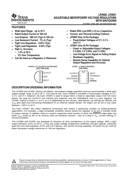
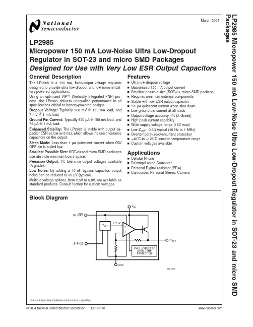
LP2985Micropower 150mA Low-Noise Ultra Low-Dropout Regulator in SOT-23and micro SMD PackagesDesigned for Use with Very Low ESR Output CapacitorsGeneral DescriptionThe LP2985is a 150mA,fixed-output voltage regulator designed to provide ultra low-dropout and low noise in bat-tery powered applications.Using an optimized VIP ™(Vertically Integrated PNP)pro-cess,the LP2985delivers unequalled performance in all specifications critical to battery-powered designs:Dropout Voltage:Typically 300mV @150mA load,and 7mV @1mA load.Ground Pin Current:Typically 850µA @150mA load,and 75µA @1mA load.Enhanced Stability:The LP2985is stable with output ca-pacitor ESR as low as 5m Ω,which allows the use of ceramic capacitors on the output.Sleep Mode:Less than 1µA quiescent current when ON/OFF pin is pulled low.Smallest Possible Size:SOT-23and micro SMD packages use absolute minimum board space.Precision Output:1%tolerance output voltages available (A grade).Low Noise:By adding a 10nF bypass capacitor,output noise can be reduced to 30µV (typical).Multiple voltage options,from 2.5V to 5.0V,are available as standard products.Consult factory for custom voltages.Featuresn Ultra low dropout voltagen Guaranteed 150mA output currentn Smallest possible size (SOT-23,micro SMD package)n Requires minimum external components n Stable with low-ESR output capacitor n <1µA quiescent current when shut down n Low ground pin current at all loads n Output voltage accuracy 1%(A Grade)n High peak current capabilityn Wide supply voltage range (16V max)n Low Z OUT :0.3Ωtypical (10Hz to 1MHz)n Overtemperature/overcurrent protectionn −40˚C to +125˚C junction temperature range nCustom voltages availableApplicationsn Cellular Phonen Palmtop/Laptop Computern Personal Digital Assistant (PDA)nCamcorder,Personal Stereo,CameraBlock Diagram10014001VIP ™is a trademark of National Semiconductor Corporation.March 2004LP2985Micropower 150mA Low-Noise Ultra Low-Dropout Regulator in SOT-23and micro SMD Packages©2004National Semiconductor Corporation Basic Application Circuit10014002*ON/OFF input must be actively terminated.Tie to V IN if this function is not to be used.**Minimum capacitance is shown to ensure stability (may be increased without limit).Ceramic capacitor required for output (see Application Hints).***Reduces output noise (may be omitted if application is not noise critical).Use ceramic or film type with very low leakage current (see Application Hints).Connection Diagrams5-Lead Small Outline Package (M5)micro SMD,5Bump Package (BPA05,TPA05&BLA05)10014003Top ViewSee NS Package Number MF05A For ordering information see Table 110014046Note:The actual physical placement of the package marking will vary from part to part.Package marking contains date code and lot traceabilityinformation,and will vary considerably.Package marking does not correlate to device type.Top ViewSee NS Package Number BPA05,TPA05&BLA05Pin DescrptionNamePin NumberFunctionSOT-23micro SMDV IN 1C3Input VoltageGND 2A1Common Ground (device substrate)ON/OFF 3A3Logic high enable inputBYPASS 4B2Bypass capacitor for low noise operation V OUT5C1Regulated output voltageL P 2985 2Ordering InformationTABLE1.Package Marking and Ordering InformationOutput Voltage(V)Grade Order Information PackageMarkingSupplied as:5-Lead Small Outline Package(M5)For output voltages≤2.3V,refer to LP2985LV datasheet.2.5A LP2985AIM5X-2.5LAUA3000Units on Tape and Reel2.5A LP2985AIM5-2.5LAUA1000Units on Tape and Reel2.5STD LP2985IM5X-2.5LAUB3000Units on Tape and Reel2.5STD LP2985IM5-2.5LAUB1000Units on Tape and Reel2.6A LP2985AIM5X-2.6LCEA3000Units on Tape and Reel2.6A LP2985AIM5-2.6LCEA1000Units on Tape and Reel2.6STD LP2985IM5X-2.6LCEB3000Units on Tape and Reel2.6STD LP2985IM5-2.6LCEB1000Units on Tape and Reel2.7A LP2985AIM5X-2.7LALA3000Units on Tape and Reel2.7A LP2985AIM5-2.7LALA1000Units on Tape and Reel2.7STD LP2985IM5X-2.7LALB3000Units on Tape and Reel2.7STD LP2985IM5-2.7LALB1000Units on Tape and Reel2.8A LP2985AIM5X-2.8L0KA3000Units on Tape and Reel2.8A LP2985AIM5-2.8L0KA1000Units on Tape and Reel2.8STD LP2985IM5X-2.8L0KB3000Units on Tape and Reel2.8STD LP2985IM5-2.8L0KB1000Units on Tape and Reel2.9A LP2985AIM5X-2.9LAXA3000Units on Tape and Reel2.9A LP2985AIM5-2.9LAXA1000Units on Tape and Reel2.9STD LP2985IM5X-2.9LAXB3000Units on Tape and Reel2.9STD LP2985IM5-2.9LAXB1000Units on Tape and Reel3.0A LP2985AIM5X-3.0L0OA3000Units on Tape and Reel3.0A LP2985AIM5-3.0L0OA1000Units on Tape and Reel3.0STD LP2985IM5X-3.0L0OB3000Units on Tape and Reel3.0STD LP2985IM5-3.0L0OB1000Units on Tape and Reel3.1A LP2985AIM5X-3.1L0PA3000Units on Tape and Reel3.1A LP2985AIM5-3.1L0PA1000Units on Tape and Reel3.1STD LP2985IM5X-3.1L0PB3000Units on Tape and Reel3.1STD LP2985IM5-3.1L0PB1000Units on Tape and Reel3.2A LP2985AIM5X-3.2L0QA3000Units on Tape and Reel3.2A LP2985AIM5-3.2L0QA1000Units on Tape and Reel3.2STD LP2985IM5X-3.2L0QB3000Units on Tape and Reel3.2STD LP2985IM5-3.2L0QB1000Units on Tape and Reel3.3A LP2985AIM5X-3.3L0RA3000Units on Tape and Reel3.3A LP2985AIM5-3.3L0RA1000Units on Tape and Reel3.3STD LP2985IM5X-3.3L0RB3000Units on Tape and Reel3.3STD LP2985IM5-3.3L0RB1000Units on Tape and Reel3.5A LP2985AIM5X-3.5LAIA3000Units on Tape and Reel3.5A LP2985AIM5-3.5LAIA1000Units on Tape and Reel3.5STD LP2985IM5X-3.5LAIB3000Units on Tape and Reel3.5STD LP2985IM5-3.5LAIB1000Units on Tape and Reel3.6A LP2985AIM5X-3.6L0SA3000Units on Tape and Reel3.6A LP2985AIM5-3.6L0SA1000Units on Tape and Reel3.6STD LP2985IM5X-3.6L0SB3000Units on Tape and Reel3.6STD LP2985IM5-3.6L0SB1000Units on Tape and Reel3.8A LP2985AIM5X-3.8L0YA3000Units on Tape and ReelLP29853Ordering Information(Continued)TABLE 1.Package Marking and Ordering Information (Continued)Output Voltage (V)Grade Order Information Package Marking Supplied as:3.8A LP2985AIM5-3.8L0YA 1000Units on Tape and Reel 3.8STD LP2985IM5X-3.8L0YB 3000Units on Tape and Reel 3.8STD LP2985IM5-3.8L0YB 1000Units on Tape and Reel4.0A LP2985AIM5X-4.0L0TA 3000Units on Tape and Reel 4.0A LP2985AIM5-4.0L0TA 1000Units on Tape and Reel 4.0STD LP2985IM5X-4.0L0TB 3000Units on Tape and Reel 4.0STD LP2985IM5-4.0L0TB 1000Units on Tape and Reel 4.5A LP2985AIM5X-4.5LA7A 3000Units on Tape and Reel 4.5A LP2985AIM5-4.5LA7A 1000Units on Tape and Reel 4.5STD LP2985IM5X-4.5LA7B 3000Units on Tape and Reel 4.5STD LP2985IM5-4.5LA7B 1000Units on Tape and Reel 4.7A LP2985AIM5X-4.7LAJA 3000Units on Tape and Reel 4.7A LP2985AIM5-4.7LAJA 1000Units on Tape and Reel 4.7STD LP2985IM5X-4.7LAJB 3000Units on Tape and Reel 4.7STD LP2985IM5-4.7LAJB 1000Units on Tape and Reel 4.8A LP2985AIM5X-4.8LAKA 3000Units on Tape and Reel 4.8A LP2985AIM5-4.8LAKA 1000Units on Tape and Reel 4.8STD LP2985IM5X-4.8LAKB 3000Units on Tape and Reel 4.8STD LP2985IM5-4.8LAKB 1000Units on Tape and Reel5.0A LP2985AIM5X-5.0L0UA 3000Units on Tape and Reel 5.0A LP2985AIM5-5.0L0UA 1000Units on Tape and Reel 5.0STD LP2985IM5X-5.0L0UB 3000Units on Tape and Reel 5.0STD LP2985IM5-5.0L0UB 1000Units on Tape and Reel 5.3A LP2985AIM5X-5.3LFYA 3000Units on Tape and Reel 5.3A LP2985AIM5-5.3LFYA 1000Units on Tape and Reel 5.3STD LP2985IM5X-5.3LFYB 3000Units on Tape and Reel 5.3STD LP2985IM5-5.3LFYB 1000Units on Tape and Reel6.1A LP2985AIM5X-6.1LF6A 3000Units on Tape and Reel 6.1A LP2985AIM5-6.1LF6A 1000Units on Tape and Reel 6.1STD LP2985IM5X-6.1LF6B 3000Units on Tape and Reel 6.1STD LP2985IM5-6.1LF6B 1000Units on Tape and Reel 12(Note 11)A LP2985AIM5X-12LH1A 3000Units on Tape and Reel 12(Note 11)A LP2985AIM5-12LH1A 1000Units on Tape and Reel 12(Note 11)STD LP2985IM5X-12LH1B 3000Units on Tape and Reel 12(Note 11)STDLP2985IM5-12LH1B1000Units on Tape and Reelmicro SMD,5Bump Package (BPA05-170µm ball)2.4A LP2985AIBP-2.4250Units on Tape and Reel 2.4A LP2985AIBPX-2.43000Units on Tape and Reel 2.4STD LP2985IBP-2.4250Units on Tape and Reel 2.4STD LP2985IBPX-2.43000Units on Tape and Reel 2.5A LP2985AIBP-2.5250Units on Tape and Reel 2.5A LP2985AIBPX-2.53000Units on Tape and Reel 2.5STD LP2985IBP-2.5250Units on Tape and Reel 2.5STDLP2985IBPX-2.53000Units on Tape and ReelL P 29854Ordering Information(Continued)TABLE1.Package Marking and Ordering Information(Continued)Output Voltage(V)Grade Order Information PackageMarkingSupplied as:2.6A LP2985AIBP-2.6250Units on Tape and Reel2.6A LP2985AIBPX-2.63000Units on Tape and Reel2.6STD LP2985IBP-2.6250Units on Tape and Reel2.6STD LP2985IBPX-2.63000Units on Tape and Reel2.8A LP2985AIBP-2.8250Units on Tape and Reel2.8A LP2985AIBPX-2.83000Units on Tape and Reel2.8STD LP2985IBP-2.8250Units on Tape and Reel2.8STD LP2985IBPX-2.83000Units on Tape and Reel2.9A LP2985AIBP-2.9250Units on Tape and Reel2.9A LP2985AIBPX-2.93000Units on Tape and Reel2.9STD LP2985IBP-2.9250Units on Tape and Reel2.9STD LP2985IBPX-2.93000Units on Tape and Reel3.0A LP2985AIBP-3.0250Units on Tape and Reel3.0A LP2985AIBPX-3.03000Units on Tape and Reel3.0STD LP2985IBP-3.0250Units on Tape and Reel3.0STD LP2985IBPX-3.03000Units on Tape and Reel3.3A LP2985AIBP-3.3250Units on Tape and Reel3.3A LP2985AIBPX-3.33000Units on Tape and Reel3.3STD LP2985IBPX-3.3250Units on Tape and Reel3.3STD LP2985IBPX-3.33000Units on Tape and Reel3.6A LP2985AIBP-3.6250Units on Tape and Reel3.6A LP2985AIBPX-3.63000Units on Tape and Reel3.6STD LP2985IBP-3.6250Units on Tape and Reel3.6STD LP2985IBPX-3.63000Units on Tape and Reel4.0A LP2985AIBP-4.0250Units on Tape and Reel4.0A LP2985AIBPX-4.03000Units on Tape and Reel4.0STD LP2985IBP-4.0250Units on Tape and Reel4.0STD LP2985IBPX-4.03000Units on Tape and Reel5.0A LP2985AIBP-5.0250Units on Tape and Reel5.0A LP2985AIBPX-5.03000Units on Tape and Reel5.0STD LP2985IBP-5.0250Units on Tape and Reel5.0STD LP2985IBPX-5.03000Units on Tape and Reelmicro SMD,5Bump Package(TPA05-170µm ball)2.5A LP2985AITP-2.5250Units on Tape and Reel2.5A LP2985AITPX-2.53000Units on Tape and Reel2.5STD LP2985ITP-2.5250Units on Tape and Reel2.5STD LP2985ITPX-2.53000Units on Tape and Reel2.7A LP2985AITP-2.7250Units on Tape and Reel2.7A LP2985AITPX-2.73000Units on Tape and Reel2.7STD LP2985ITP-2.7250Units on Tape and Reel2.7STD LP2985ITPX-2.73000Units on Tape and Reel2.8A LP2985AITP-2.8250Units on Tape and Reel2.8A LP2985AITPX-2.83000Units on Tape and Reel2.8STD LP2985ITP-2.8250Units on Tape and Reel2.8STD LP2985ITPX-2.83000Units on Tape and Reel5.0A LP2985AITP-5.0250Units on Tape and Reel5.0A LP2985AITPX-5.03000Units on Tape and ReelLP29855Ordering Information(Continued)TABLE 1.Package Marking and Ordering Information (Continued)Output Voltage (V)Grade Order Information Package MarkingSupplied as:5.0STD LP2985ITP-5.0250Units on Tape and Reel 5.0STD LP2985ITPX-5.03000Units on Tape and Reel micro SMD,5Bump Package (BLA05-300µm ball)2.85A LP2985AIBL-285250Units on Tape and Reel 2.85A LP2985AIBLX-2853000Units on Tape and Reel 2.85STD LP2985IBL-285250Units on Tape and Reel 2.85STD LP2985IBLX-2853000Units on Tape and Reel3.0A LP2985AIBL-3.0250Units on Tape and Reel 3.0A LP2985AIBLX-3.03000Units on Tape and Reel 3.0STD LP2985IBL-3.0250Units on Tape and Reel 3.0STD LP2985IBLX-3.03000Units on Tape and Reel 3.3A LP2985AIBL-3.3250Units on Tape and Reel 3.3A LP2985AIBLX-3.33000Units on Tape and Reel 3.3STD LP2985IBL-3.3250Units on Tape and Reel 3.3STDLP2985IBLX-3.33000Units on Tape and ReelL P 2985 6Absolute Maximum Ratings (Note 1)If Military/Aerospace specified devices are required,please contact the National Semiconductor Sales Office/Distributors for availability and specifications.Storage Temperature Range −65˚C to +150˚C Operating Junction Temperature Range−40˚C to +125˚CLead Temp.(Soldering,5sec.)260˚C ESD Rating (Note 2)2kVPower Dissipation (Note 3)Internally LimitedInput Supply Voltage (Survival)−0.3V to +16V Input Supply Voltage (Operating) 2.5V to +16V Shutdown Input Voltage (Survival)−0.3V to +16V Output Voltage (Survival,(Note 4))−0.3V to +9V I OUT (Survival)Short Circuit Protected Input-Output Voltage (Survival,−0.3V to +16V(Note 5))Electrical Characteristics (Note 10)Limits in standard typeface are for T J =25˚C.and limits in boldface type apply over the full operating temperature range.Un-less otherwise specified:V IN =V O (NOM)+1V,I L =1mA,C IN =1µF,C OUT =4.7µF,V ON/OFF =2V.Symbol Parameter ConditionsTypLP2985AI-X.XLP2985I-X.X Units(Note 6)(Note 6)Min Max Min Max ∆V OOutput Voltage ToleranceI L =1mA−1.0 1.0−1.5 1.5%V NOM 1mA ≤I L ≤50mA −1.5 1.5−2.5 2.5−2.5 2.5−3.5 3.51mA ≤I L ≤150mA−2.5 2.5−3.0 3.0−3.53.5−4.04.0Output Voltage V O (NOM)+1V ≤V IN ≤16V0.0070.0140.014%/V Line Regulation0.0320.032V IN –V ODropout Voltage (Note 7)I L =0133mV 55I L =1mA 710101515I L =10mA 4060609090I L =50mA 120150*********I L =150mA280350350575575I GNDGround Pin Current (Note 11)I L =0659595µA 125125I L =1mA 75110110170170I L =10mA 120220220400400I L =50mA 35060060010001000I L =150mA 8501500150025002500V ON/OFF <0.3V 0.010.80.8V ON/OFF <0.15V0.0522V ON/OFF ON/OFF Input Voltage (Note 8)High =O/P ON 1.4 1.61.6V Low =O/P OFF 0.550.150.15I ON/OFFON/OFF Input CurrentV ON/OFF =00.01−2−2µA V ON/OFF =5V51515LP29857Electrical Characteristics (Note 10)(Continued)Limits in standard typeface are for T J =25˚C.and limits in boldface type apply over the full operating temperature range.Un-less otherwise specified:V IN =V O (NOM)+1V,I L =1mA,C IN =1µF,C OUT =4.7µF,V ON/OFF =2V.SymbolParameter ConditionsTypLP2985AI-X.XLP2985I-X.X Units(Note 6)(Note 6)MinMaxMinMaxe nOutput Noise BW =300Hz to 50kHz,Voltage (RMS)C OUT =10µF 30µVC BYPASS =10nFRipple Rejectionf =1kHz,C BYPASS =10nF 45dB C OUT =10µFI O (SC)Short Circuit Current R L =0(Steady State)400mA (Note 9)I O (PK)Peak Output CurrentV OUT ≥V o (NOM)−5%350mANote 1:“Absolute Maximum Ratings”indicate limits beyond which damage to the component may occur.Electrical specifications do not apply when operating the device outside of its rated operating conditions.Note 2:The ESD rating of pins 3and 4for the SOT-23package,or pins 5and 2for the micro SMD package,is 1kV.Note 3:The maximum allowable power dissipation is a function of the maximum junction temperature,T J (MAX),the junction-to-ambient thermal resistance,θJ-A ,and the ambient temperature,T A .The maximum allowable power dissipation at any ambient temperture is calculated using:Where the value of θJ-A for the SOT-23package is 220˚C/W in a typical PC board mounting and the micro SMD package is 225˚C/W.Exceeding the maximum allowable dissipation will cause excessive die temperature,and the regulator will go into thermal shutdown.Note 4:For 12V option,output voltage survival:-0.3to +16V.If used in a dual-supply system where the regulator load is returned to a negative supply,the LP2985output must be diode-clamped to ground.Note 5:The output PNP structure contains a diode between the V IN to V OUT terminals that is normally reverse-biased.Reversing the polarity from V IN to V OUT will turn on this diode.Note 6:Limits are 100%production tested at 25˚C.Limits over the operating temperature range are guaranteed through correlation using Statistical Quality Control (SQC)methods.The limits are used to calculate National’s Average Outgoing Quality Level (AOQL).Note 7:Dropout voltage is defined as the input to output differential at which the output voltage drops 100mV below the value measured with a 1V differential.Note 8:The ON/OFF input must be properly driven to prevent possible misoperation.For details,refer to Application Hints.Note 9:The LP2985has foldback current limiting which allows a high peak current when V OUT >0.5V,and then reduces the maximum output current as V OUT is forced to ground (see Typical Performance Characteristics curves).Note 10:Exposing the micro SMD device to direct sunlight will cause misoperation.See Application Hints for additional information.Note 11:For 12V option,add 50µA to all ON state quiescent current values.L P 2985 8Typical Performance CharacteristicsUnless otherwise specified:C IN =1µF,C OUT =4.7µF,V IN =V OUT (NOM)+1,T A =25˚C,ON/OFF pin is tied to V IN .V OUT vs TemperatureShort-Circuit Current1001400810014009Short-Circuit Current Short Circuit Current vs Output Voltage1001401010014011Ripple Rejection Ripple Rejection1001401310014014LP29859Typical Performance Characteristics Unless otherwise specified:C IN =1µF,C OUT =4.7µF,V IN =V OUT (NOM)+1,T A =25˚C,ON/OFF pin is tied to V IN .(Continued)Ripple RejectionRipple Rejection1001401510014016Ripple Rejection Ripple Rejection1001401710014018Ripple Rejection Ripple Rejection1001401910014023L P 2985 10Typical Performance Characteristics Unless otherwise specified:C IN =1µF,C OUT =4.7µF,V IN =V OUT (NOM)+1,T A =25˚C,ON/OFF pin is tied to V IN .(Continued)Ripple Rejection Output Impedance vs Frequency1001402210014020Output Impedance vs Frequency Output Noise Density1001402110014024Output Noise Density Ground Pin vs Load Current1001402510014026LP2985Typical Performance Characteristics Unless otherwise specified:C IN =1µF,C OUT =4.7µF,V IN =V OUT (NOM)+1,T A =25˚C,ON/OFF pin is tied to V IN .(Continued)Dropout Voltage vs Temperature Input Current vs Pin1001402710014029GND Pin Current vs Temperature Instantaneous Short Circuit Current1001403010014031Load Transient Response Load Transient Response1001403210014033L P 2985Typical Performance Characteristics Unless otherwise specified:C IN =1µF,C OUT =4.7µF,V IN =V OUT (NOM)+1,T A =25˚C,ON/OFF pin is tied to V IN .(Continued)Load Transient Response Line Transient Response1001403410014035Line Transient Response Line Transient Response1001403610014037Line Transient Response Turn-On Time1001403810014039LP2985Typical Performance Characteristics Unless otherwise specified:C IN =1µF,C OUT =4.7µF,V IN =V OUT (NOM)+1,T A =25˚C,ON/OFF pin is tied to V IN .(Continued)Turn-On Time Turn-On Time1001404010014041Turn-On Time10014042L P 2985Application HintsEXTERNAL CAPACITORSLike any low-dropout regulator,the LP2985requires external capacitors for regulator stability.These capacitors must be correctly selected for good performance.Input CapacitorAn input capacitor whose capacitance is≥1µF is required between the LP2985input and ground(the amount of ca-pacitance may be increased without limit).This capacitor must be located a distance of not more than1 cm from the input pin and returned to a clean analog ground. Any good quality ceramic,tantalum,or film capacitor may be used at the input.Important:Tantalum capacitors can suffer catastrophic fail-ure due to surge current when connected to a low-impedance source of power(like a battery or very large capacitor).If a Tantalum capacitor is used at the input,it must be guaranteed by the manufacturer to have a surge current rating sufficient for the application.There are no requirements for ESR on the input capacitor, but tolerance and temperature coefficient must be consid-ered when selecting the capacitor to ensure the capacitance will be≥1µF over the entire operating temperature range. Output CapacitorThe LP2985is designed specifically to work with ceramic output capacitors,utilizing circuitry which allows the regula-tor to be stable across the entire range of output current with an output capacitor whose ESR is as low as5mΩ.It may also be possible to use Tantalum or film capacitors at the output,but these are not as attractive for reasons of size and cost(see next section Capacitor Characteristics).The output capacitor must meet the requirement for mini-mum amount of capacitance and also have an ESR(equiva-lent series resistance)value which is within the stable range. Curves are provided which show the stable ESR range as a function of load current(see ESR graph below).10014007 Important:The output capacitor must maintain its ESR within the stable region over the full operating temperature range of the application to assure stability.The LP2985requires a minimum of2.2µF on the output (output capacitor size can be increased without limit).It is important to remember that capacitor tolerance and variation with temperature must be taken into consideration when selecting an output capacitor so that the minimum required amount of output capacitance is provided over the full operating temperature range.It should be noted that ceramic capacitors can exhibit large changes in capacitancewith temperature(see next section,Capacitor Characteris-tics).The output capacitor must be located not more than1cmfrom the output pin and returned to a clean analog ground.Noise Bypass CapacitorConnecting a10nF capacitor to the Bypass pin significantly reduces noise on the regulator output.It should be noted thatthe capacitor is connected directly to a high-impedance cir-cuit in the bandgap reference.Because this circuit has only a few microamperes flowing init,any significant loading on this node will cause a change inthe regulated output voltage.For this reason,DC leakagecurrent through the noise bypass capacitor must never ex-ceed100nA,and should be kept as low as possible for bestoutput voltage accuracy.The types of capacitors best suited for the noise bypass capacitor are ceramic and film.High-quality ceramic capaci-tors with either NPO or COG dielectric typically have verylow leakage.10nF polypropolene and polycarbonate film capacitors are available in small surface-mount packagesand typically have extremely low leakage current.CAPACITOR CHARACTERISTICSThe LP2985was designed to work with ceramic capacitorson the output to take advantage of the benefits they offer:for capacitance values in the2.2µF to4.7µF range,ceramicsare the least expensive and also have the lowest ESRvalues(which makes them best for eliminating high-frequency noise).The ESR of a typical 2.2µF ceramic capacitor is in the range of10mΩto20mΩ,which easilymeets the ESR limits required for stability by the LP2985.One disadvantage of ceramic capacitors is that their capaci-tance can vary with temperature.Most large value ceramic capacitors(≥2.2µF)are manufactured with the Z5U or Y5V temperature characteristic,which results in the capacitance dropping by more than50%as the temperature goes from25˚C to85˚C.This could cause problems if a2.2µF capacitor were usedon the output since it will drop down to approximately1µF athigh ambient temperatures(which could cause the LM2985to oscillate).If Z5U or Y5V capacitors are used on the output,a minimum capacitance value of4.7µF must be observed.A better choice for temperature coefficient in ceramic capaci-tors is X7R,which holds the capacitance within±15%.Un-fortunately,the larger values of capacitance are not offeredby all manufacturers in the X7R dielectric.TantalumTantalum capacitors are less desirable than ceramics for useas output capacitors because they are more expensive when comparing equivalent capacitance and voltage ratings in the1µF to4.7µF range.Another important consideration is that Tantalum capacitorshave higher ESR values than equivalent size ceramics.Thismeans that while it may be possible to find a Tantalum capacitor with an ESR value within the stable range,it wouldhave to be larger in capacitance(which means bigger andmore costly)than a ceramic capacitor with the same ESR value.LP2985Application Hints (Continued)It should also be noted that the ESR of a typical Tantalum willincrease about 2:1as the temperature goes from 25˚C downto −40˚C,so some guard band must be allowed.On/off Input OperationThe LP2985is shut off by driving the ON/OFF input low,andturned on by pulling it high.If this feature is not to be used,the ON/OFF input should be tied to V IN to keep the regulatoroutput on at all times.To assure proper operation,the signal source used to drivethe ON/OFF input must be able to swing above and belowthe specified turn-on/turn-off voltage thresholds listed in theElectrical Characteristics section under V ON/OFF .To preventmis-operation,the turn-on (and turn-off)voltage signals ap-plied to the ON/OFF input must have a slew rate which is≥40mV/µs.Caution:the regulator output voltage can not be guaranteedif a slow-moving AC (or DC)signal is applied that is in therange between the specified turn-on and turn-off voltageslisted under the electrical specification V ON/OFF (see Electri-cal Characteristics).REVERSE INPUT-OUTPUT VOLTAGEThe PNP power transistor used as the pass element in theLP2985has an inherent diode connected between the regu-lator output and input.During normal operation (where theinput voltage is higher than the output)this diode is reverse-biased.However,if the output is pulled above the input,this diodewill turn ON and current will flow into the regulator output.In such cases,a parasitic SCR can latch which will allow a high current to flow into V IN (and out the ground pin),which can damage the part.In any application where the output may be pulled above the input,an external Schottky diode must be connected from V IN to V OUT (cathode on V IN ,anode on V OUT ),to limit the reverse voltage across the LP2985to 0.3V (see Absolute Maximum Ratings).MICRO SMD MOUNTING The micro SMD package requires specific mounting tech-niques which are detailed in National Semiconductor Appli-cation Note #1112.Referring to the section Surface Mount Technology (SMT)Assembly Considerations ,it should be noted that the pad style which must be used with the 5-pin package is the NSMD (non-solder mask defined)type.For best results during assembly,alignment ordinals on the PC board may be used to facilitate placement of the micro SMD device.MICRO SMD LIGHT SENSITIVITY Exposing the micro SMD device to direct sunlight will cause misoperation of the device.Light sources such as Halogen lamps can also affect electrical performance if brought near to the device.The wavelenghts which have the most detrimental effect are reds and infra-reds,which means that the fluorescent light-ing used inside most buildings has very little effect on per-formance.A micro SMD test board was brought to within 1cm of a fluorescent desk lamp and the effect on the regu-lated output voltage was negligible,showing a deviation of less than 0.1%from nominal.L P 2985Physical Dimensions inches(millimeters)unless otherwise noted5-Lead Small Outline Package(M5)NS Package Number MF05AFor Order Numbers,refer to Table1in the“Ordering Information”section of this document.LP2985。