
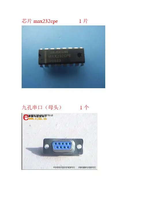
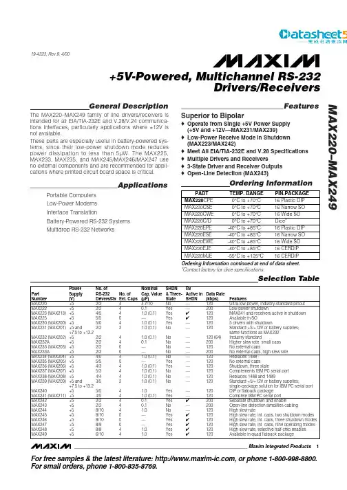
max232串口通信电路清单
- 格式:doc
- 大小:206.00 KB
- 文档页数:2
General DescriptionThe MAX220–MAX249 family of line drivers/receivers is intended for all EIA/TIA-232E and V.28/V.24 communica-tions interfaces, particularly applications where ±12V is not available.These parts are especially useful in battery-powered sys-tems, since their low-power shutdown mode reduces power dissipation to less than 5µW. The MAX225,MAX233, MAX235, and MAX245/MAX246/MAX247 use no external components and are recommended for appli-cations where printed circuit board space is critical.________________________ApplicationsPortable Computers Low-Power Modems Interface TranslationBattery-Powered RS-232 Systems Multidrop RS-232 Networks____________________________Features Superior to Bipolaro Operate from Single +5V Power Supply (+5V and +12V—MAX231/MAX239)o Low-Power Receive Mode in Shutdown (MAX223/MAX242)o Meet All EIA/TIA-232E and V.28 Specifications o Multiple Drivers and Receiverso 3-State Driver and Receiver Outputs o Open-Line Detection (MAX243)Ordering InformationOrdering Information continued at end of data sheet.*Contact factory for dice specifications.MAX220–MAX249+5V-Powered, Multichannel RS-232Drivers/Receivers________________________________________________________________Maxim Integrated Products 1Selection Table19-4323; Rev 9; 4/00Power No. ofNominalSHDN RxPart Supply RS-232No. of Cap. Value & Three-Active in Data Rate Number (V)Drivers/Rx Ext. Caps (µF)State SHDN (kbps)FeaturesMAX220+52/24 4.7/10No —120Ultra-low-power, industry-standard pinout MAX222+52/2 4 0.1Yes —200Low-power shutdownMAX223 (MAX213)+54/54 1.0 (0.1)Yes ✔120MAX241 and receivers active in shutdown MAX225+55/50—Yes ✔120Available in SOMAX230 (MAX200)+55/04 1.0 (0.1)Yes —120 5 drivers with shutdownMAX231 (MAX201)+5 and2/2 2 1.0 (0.1)No —120Standard +5/+12V or battery supplies; +7.5 to +13.2same functions as MAX232MAX232 (MAX202)+52/24 1.0 (0.1)No —120 (64)Industry standardMAX232A+52/240.1No —200Higher slew rate, small caps MAX233 (MAX203)+52/20— No —120No external capsMAX233A+52/20—No —200No external caps, high slew rate MAX234 (MAX204)+54/04 1.0 (0.1)No —120Replaces 1488MAX235 (MAX205)+55/50—Yes —120No external capsMAX236 (MAX206)+54/34 1.0 (0.1)Yes —120Shutdown, three stateMAX237 (MAX207)+55/34 1.0 (0.1)No —120Complements IBM PC serial port MAX238 (MAX208)+54/44 1.0 (0.1)No —120Replaces 1488 and 1489MAX239 (MAX209)+5 and3/52 1.0 (0.1)No —120Standard +5/+12V or battery supplies;+7.5 to +13.2single-package solution for IBM PC serial port MAX240+55/54 1.0Yes —120DIP or flatpack package MAX241 (MAX211)+54/54 1.0 (0.1)Yes —120Complete IBM PC serial port MAX242+52/240.1Yes ✔200Separate shutdown and enableMAX243+52/240.1No —200Open-line detection simplifies cabling MAX244+58/104 1.0No —120High slew rateMAX245+58/100—Yes ✔120High slew rate, int. caps, two shutdown modes MAX246+58/100—Yes ✔120High slew rate, int. caps, three shutdown modes MAX247+58/90—Yes ✔120High slew rate, int. caps, nine operating modes MAX248+58/84 1.0Yes ✔120High slew rate, selective half-chip enables MAX249+56/1041.0Yes✔120Available in quad flatpack packageFor free samples & the latest literature: , or phone 1-800-998-8800.For small orders, phone 1-800-835-8769.M A X 220–M A X 249+5V-Powered, Multichannel RS-232Drivers/ReceiversABSOLUTE MAXIMUM RATINGS—MAX220/222/232A/233A/242/243ELECTRICAL CHARACTERISTICS—MAX220/222/232A/233A/242/243(V CC = +5V ±10%, C1–C4 = 0.1µF‚ MAX220, C1 = 0.047µF, C2–C4 = 0.33µF, T A = T MIN to T MAX ‚ unless otherwise noted.)Note 1:Input voltage measured with T OUT in high-impedance state, SHDN or V CC = 0V.Note 2:For the MAX220, V+ and V- can have a maximum magnitude of 7V, but their absolute difference cannot exceed 13V.Stresses beyond those listed under “Absolute Maximum Ratings” may cause permanent damage to the device. These are stress ratings only, and functional operation of the device at these or any other conditions beyond those indicated in the operational sections of the specifications is not implied. Exposure to absolute maximum rating conditions for extended periods may affect device reliability.Supply Voltage (V CC )...............................................-0.3V to +6V Input VoltagesT IN ..............................................................-0.3V to (V CC - 0.3V)R IN (Except MAX220)........................................................±30V R IN (MAX220).....................................................................±25V T OUT (Except MAX220) (Note 1).......................................±15V T OUT (MAX220)...............................................................±13.2V Output VoltagesT OUT ...................................................................................±15V R OUT .........................................................-0.3V to (V CC + 0.3V)Driver/Receiver Output Short Circuited to GND.........Continuous Continuous Power Dissipation (T A = +70°C)16-Pin Plastic DIP (derate 10.53mW/°C above +70°C)....842mW 18-Pin Plastic DIP (derate 11.11mW/°C above +70°C)....889mW20-Pin Plastic DIP (derate 8.00mW/°C above +70°C)..440mW 16-Pin Narrow SO (derate 8.70mW/°C above +70°C)...696mW 16-Pin Wide SO (derate 9.52mW/°C above +70°C)......762mW 18-Pin Wide SO (derate 9.52mW/°C above +70°C)......762mW 20-Pin Wide SO (derate 10.00mW/°C above +70°C)....800mW 20-Pin SSOP (derate 8.00mW/°C above +70°C)..........640mW 16-Pin CERDIP (derate 10.00mW/°C above +70°C).....800mW 18-Pin CERDIP (derate 10.53mW/°C above +70°C).....842mW Operating Temperature RangesMAX2_ _AC_ _, MAX2_ _C_ _.............................0°C to +70°C MAX2_ _AE_ _, MAX2_ _E_ _..........................-40°C to +85°C MAX2_ _AM_ _, MAX2_ _M_ _.......................-55°C to +125°C Storage Temperature Range.............................-65°C to +160°C Lead Temperature (soldering, 10sec).............................+300°CMAX220–MAX249+5V-Powered, Multichannel RS-232Drivers/Receivers_______________________________________________________________________________________3Note 3:MAX243 R2OUT is guaranteed to be low when R2IN is ≥0V or is floating.ELECTRICAL CHARACTERISTICS—MAX220/222/232A/233A/242/243 (continued)(V= +5V ±10%, C1–C4 = 0.1µF‚ MAX220, C1 = 0.047µF, C2–C4 = 0.33µF, T = T to T ‚ unless otherwise noted.)M A X 220–M A X 249+5V-Powered, Multichannel RS-232Drivers/Receivers 4_________________________________________________________________________________________________________________________________Typical Operating CharacteristicsMAX220/MAX222/MAX232A/MAX233A/MAX242/MAX243108-1051525OUTPUT VOLTAGE vs. LOAD CURRENT-4-6-8-2642LOAD CURRENT (mA)O U T P U T V O L T A G E (V )1002011104104060AVAILABLE OUTPUT CURRENTvs. DATA RATE65798DATA RATE (kbits/sec)O U T P U T C U R R E N T (m A )203050+10V-10VMAX222/MAX242ON-TIME EXITING SHUTDOWN+5V +5V 0V0V 500µs/div V +, V - V O L T A G E (V )MAX220–MAX249+5V-Powered, Multichannel RS-232Drivers/Receivers_______________________________________________________________________________________5V CC ...........................................................................-0.3V to +6V V+................................................................(V CC - 0.3V) to +14V V-............................................................................+0.3V to -14V Input VoltagesT IN ............................................................-0.3V to (V CC + 0.3V)R IN ......................................................................................±30V Output VoltagesT OUT ...................................................(V+ + 0.3V) to (V- - 0.3V)R OUT .........................................................-0.3V to (V CC + 0.3V)Short-Circuit Duration, T OUT ......................................Continuous Continuous Power Dissipation (T A = +70°C)14-Pin Plastic DIP (derate 10.00mW/°C above +70°C)....800mW 16-Pin Plastic DIP (derate 10.53mW/°C above +70°C)....842mW 20-Pin Plastic DIP (derate 11.11mW/°C above +70°C)....889mW 24-Pin Narrow Plastic DIP(derate 13.33mW/°C above +70°C)..........1.07W24-Pin Plastic DIP (derate 9.09mW/°C above +70°C)......500mW 16-Pin Wide SO (derate 9.52mW/°C above +70°C).........762mW20-Pin Wide SO (derate 10 00mW/°C above +70°C).......800mW 24-Pin Wide SO (derate 11.76mW/°C above +70°C).......941mW 28-Pin Wide SO (derate 12.50mW/°C above +70°C) .............1W 44-Pin Plastic FP (derate 11.11mW/°C above +70°C).....889mW 14-Pin CERDIP (derate 9.09mW/°C above +70°C)..........727mW 16-Pin CERDIP (derate 10.00mW/°C above +70°C)........800mW 20-Pin CERDIP (derate 11.11mW/°C above +70°C)........889mW 24-Pin Narrow CERDIP(derate 12.50mW/°C above +70°C)..............1W24-Pin Sidebraze (derate 20.0mW/°C above +70°C)..........1.6W 28-Pin SSOP (derate 9.52mW/°C above +70°C).............762mW Operating Temperature RangesMAX2 _ _ C _ _......................................................0°C to +70°C MAX2 _ _ E _ _...................................................-40°C to +85°C MAX2 _ _ M _ _ ...............................................-55°C to +125°C Storage Temperature Range.............................-65°C to +160°C Lead Temperature (soldering, 10sec).............................+300°CABSOLUTE MAXIMUM RATINGS—MAX223/MAX230–MAX241ELECTRICAL CHARACTERISTICS—MAX223/MAX230–MAX241(MAX223/230/232/234/236/237/238/240/241, V CC = +5V ±10; MAX233/MAX235, V CC = 5V ±5%‚ C1–C4 = 1.0µF; MAX231/MAX239,V CC = 5V ±10%; V+ = 7.5V to 13.2V; T A = T MIN to T MAX ; unless otherwise noted.)Stresses beyond those listed under “Absolute Maximum Ratings” may cause permanent damage to the device. These are stress ratings only, and functional operation of the device at these or any other conditions beyond those indicated in the operational sections of the specifications is not implied. Exposure to absolute maximum rating conditions for extended periods may affect device reliability.M A X 220–M A X 249+5V-Powered, Multichannel RS-232Drivers/Receivers 6_______________________________________________________________________________________ELECTRICAL CHARACTERISTICS—MAX223/MAX230–MAX241 (continued)(MAX223/230/232/234/236/237/238/240/241, V CC = +5V ±10; MAX233/MAX235, V CC = 5V ±5%‚ C1–C4 = 1.0µF; MAX231/MAX239,V CC = 5V ±10%; V+ = 7.5V to 13.2V; T A = T MIN to T MAX ; unless otherwise noted.)MAX220–MAX249+5V-Powered, Multichannel RS-232Drivers/Receivers_______________________________________________________________________________________78.56.54.55.5TRANSMITTER OUTPUT VOLTAGE (V OH ) vs. V CC7.08.0V CC (V)V O H (V )5.07.57.46.02500TRANSMITTER OUTPUT VOLTAGE (V OH )vs. LOAD CAPACITANCE AT DIFFERENT DATA RATES6.46.27.27.0LOAD CAPACITANCE (pF)V O H (V )1500100050020006.86.612.04.02500TRANSMITTER SLEW RATE vs. LOAD CAPACITANCE6.05.011.09.010.0LOAD CAPACITANCE (pF)S L E W R A T E (V /µs )1500100050020008.07.0-6.0-9.04.55.5TRANSMITTER OUTPUT VOLTAGE (V OL ) vs. V CC-8.0-8.5-6.5-7.0V CC (V)V O L (V )5.0-7.5-6.0-7.62500TRANSMITTER OUTPUT VOLTAGE (V OL )vs. LOAD CAPACITANCE AT DIFFERENT DATA RATES-7.0-7.2-7.4-6.2-6.4LOAD CAPACITANCE (pF)V O L (V )150010005002000-6.6-6.810-105101520253035404550TRANSMITTER OUTPUT VOLTAGE (V+, V-)vs. LOAD CURRENT-2-6-4-886CURRENT (mA)V +, V- (V )420__________________________________________Typical Operating CharacteristicsMAX223/MAX230–MAX241*SHUTDOWN POLARITY IS REVERSED FOR NON MAX241 PARTSV+, V- WHEN EXITING SHUTDOWN(1µF CAPACITORS)MAX220-13SHDN*V-O V+500ms/divM A X 220–M A X 249+5V-Powered, Multichannel RS-232Drivers/Receivers 8_______________________________________________________________________________________ABSOLUTE MAXIMUM RATINGS—MAX225/MAX244–MAX249ELECTRICAL CHARACTERISTICS—MAX225/MAX244–MAX249(MAX225, V CC = 5.0V ±5%; MAX244–MAX249, V CC = +5.0V ±10%, external capacitors C1–C4 = 1µF; T A = T MIN to T MAX ; unless oth-erwise noted.)Note 4:Input voltage measured with transmitter output in a high-impedance state, shutdown, or V CC = 0V.Stresses beyond those listed under “Absolute Maximum Ratings” may cause permanent damage to the device. These are stress ratings only, and functional operation of the device at these or any other conditions beyond those indicated in the operational sections of the specifications is not implied. Exposure to absolute maximum rating conditions for extended periods may affect device reliability.Supply Voltage (V CC )...............................................-0.3V to +6V Input VoltagesT IN ‚ ENA , ENB , ENR , ENT , ENRA ,ENRB , ENTA , ENTB ..................................-0.3V to (V CC + 0.3V)R IN .....................................................................................±25V T OUT (Note 3).....................................................................±15V R OUT ........................................................-0.3V to (V CC + 0.3V)Short Circuit (one output at a time)T OUT to GND............................................................Continuous R OUT to GND............................................................ContinuousContinuous Power Dissipation (T A = +70°C)28-Pin Wide SO (derate 12.50mW/°C above +70°C).............1W 40-Pin Plastic DIP (derate 11.11mW/°C above +70°C)...611mW 44-Pin PLCC (derate 13.33mW/°C above +70°C)...........1.07W Operating Temperature RangesMAX225C_ _, MAX24_C_ _ ..................................0°C to +70°C MAX225E_ _, MAX24_E_ _ ...............................-40°C to +85°C Storage Temperature Range.............................-65°C to +160°C Lead Temperature (soldering,10sec)..............................+300°CMAX220–MAX249+5V-Powered, Multichannel RS-232Drivers/Receivers_______________________________________________________________________________________9Note 5:The 300Ωminimum specification complies with EIA/TIA-232E, but the actual resistance when in shutdown mode or V CC =0V is 10M Ωas is implied by the leakage specification.ELECTRICAL CHARACTERISTICS—MAX225/MAX244–MAX249 (continued)(MAX225, V CC = 5.0V ±5%; MAX244–MAX249, V CC = +5.0V ±10%, external capacitors C1–C4 = 1µF; T A = T MIN to T MAX ; unless oth-erwise noted.)M A X 220–M A X 249+5V-Powered, Multichannel RS-232Drivers/Receivers 10________________________________________________________________________________________________________________________________Typical Operating CharacteristicsMAX225/MAX244–MAX24918212345TRANSMITTER SLEW RATE vs. LOAD CAPACITANCE86416LOAD CAPACITANCE (nF)T R A N S M I T T E R S L E W R A T E (V /µs )14121010-105101520253035OUTPUT VOLTAGEvs. LOAD CURRENT FOR V+ AND V--2-4-6-88LOAD CURRENT (mA)O U T P U T V O L T A G E (V )64209.05.012345TRANSMITTER OUTPUT VOLTAGE (V+, V-)vs. LOAD CAPACITANCE AT DIFFERENT DATA RATES6.05.58.5LOAD CAPACITANCE (nF)V +, V (V )8.07.57.06.5MAX220–MAX249+5V-Powered, Multichannel RS-232Drivers/ReceiversFigure 1. Transmitter Propagation-Delay Timing Figure 2. Receiver Propagation-Delay TimingFigure 3. Receiver-Output Enable and Disable Timing Figure 4. Transmitter-Output Disable TimingM A X 220–M A X 249+5V-Powered, Multichannel RS-232Drivers/Receivers ENT ENR OPERATION STATUS TRANSMITTERSRECEIVERS00Normal Operation All Active All Active 01Normal Operation All Active All 3-State10Shutdown All 3-State All Low-Power Receive Mode 11ShutdownAll 3-StateAll 3-StateTable 1a. MAX245 Control Pin ConfigurationsENT ENR OPERATION STATUS TRANSMITTERS RECEIVERSTA1–TA4TB1–TB4RA1–RA5RB1–RB500Normal Operation All Active All Active All Active All Active 01Normal Operation All Active All Active RA1–RA4 3-State,RA5 Active RB1–RB4 3-State,RB5 Active 1ShutdownAll 3-StateAll 3-StateAll Low-Power Receive Mode All Low-Power Receive Mode 11Shutdown All 3-State All 3-StateRA1–RA4 3-State,RA5 Low-Power Receive ModeRB1–RB4 3-State,RB5 Low-Power Receive ModeTable 1b. MAX245 Control Pin ConfigurationsTable 1c. MAX246 Control Pin ConfigurationsENA ENB OPERATION STATUS TRANSMITTERS RECEIVERSTA1–TA4TB1–TB4RA1–RA5RB1–RB500Normal Operation All Active All Active All Active All Active 01Normal Operation All Active All 3-State All Active RB1–RB4 3-State,RB5 Active 1ShutdownAll 3-StateAll ActiveRA1–RA4 3-State,RA5 Active All Active 11Shutdown All 3-State All 3-StateRA1–RA4 3-State,RA5 Low-Power Receive ModeRB1–RB4 3-State,RA5 Low-Power Receive ModeMAX220–MAX249+5V-Powered, Multichannel RS-232Drivers/ReceiversTable 1d. MAX247/MAX248/MAX249 Control Pin ConfigurationsM A X 220–M A X 249_______________Detailed DescriptionThe MAX220–MAX249 contain four sections: dual charge-pump DC-DC voltage converters, RS-232 dri-vers, RS-232 receivers, and receiver and transmitter enable control inputs.Dual Charge-Pump Voltage ConverterThe MAX220–MAX249 have two internal charge-pumps that convert +5V to ±10V (unloaded) for RS-232 driver operation. The first converter uses capacitor C1 to dou-ble the +5V input to +10V on C3 at the V+ output. The second converter uses capacitor C2 to invert +10V to -10V on C4 at the V- output.A small amount of power may be drawn from the +10V (V+) and -10V (V-) outputs to power external circuitry (see the Typical Operating Characteristics section),except on the MAX225 and MAX245–MAX247, where these pins are not available. V+ and V- are not regulated,so the output voltage drops with increasing load current.Do not load V+ and V- to a point that violates the mini-mum ±5V EIA/TIA-232E driver output voltage when sourcing current from V+ and V- to external circuitry. When using the shutdown feature in the MAX222,MAX225, MAX230, MAX235, MAX236, MAX240,MAX241, and MAX245–MAX249, avoid using V+ and V-to power external circuitry. When these parts are shut down, V- falls to 0V, and V+ falls to +5V. For applica-tions where a +10V external supply is applied to the V+pin (instead of using the internal charge pump to gen-erate +10V), the C1 capacitor must not be installed and the SHDN pin must be tied to V CC . This is because V+is internally connected to V CC in shutdown mode.RS-232 DriversThe typical driver output voltage swing is ±8V when loaded with a nominal 5k ΩRS-232 receiver and V CC =+5V. Output swing is guaranteed to meet the EIA/TIA-232E and V.28 specification, which calls for ±5V mini-mum driver output levels under worst-case conditions.These include a minimum 3k Ωload, V CC = +4.5V, and maximum operating temperature. Unloaded driver out-put voltage ranges from (V+ -1.3V) to (V- +0.5V). Input thresholds are both TTL and CMOS compatible.The inputs of unused drivers can be left unconnected since 400k Ωinput pull-up resistors to V CC are built in (except for the MAX220). The pull-up resistors force the outputs of unused drivers low because all drivers invert.The internal input pull-up resistors typically source 12µA,except in shutdown mode where the pull-ups are dis-abled. Driver outputs turn off and enter a high-imped-ance state—where leakage current is typically microamperes (maximum 25µA)—when in shutdownmode, in three-state mode, or when device power is removed. Outputs can be driven to ±15V. The power-supply current typically drops to 8µA in shutdown mode.The MAX220 does not have pull-up resistors to force the ouputs of the unused drivers low. Connect unused inputs to GND or V CC .The MAX239 has a receiver three-state control line, and the MAX223, MAX225, MAX235, MAX236, MAX240,and MAX241 have both a receiver three-state control line and a low-power shutdown control. Table 2 shows the effects of the shutdown control and receiver three-state control on the receiver outputs.The receiver TTL/CMOS outputs are in a high-imped-ance, three-state mode whenever the three-state enable line is high (for the MAX225/MAX235/MAX236/MAX239–MAX241), and are also high-impedance whenever the shutdown control line is high.When in low-power shutdown mode, the driver outputs are turned off and their leakage current is less than 1µA with the driver output pulled to ground. The driver output leakage remains less than 1µA, even if the transmitter output is backdriven between 0V and (V CC + 6V). Below -0.5V, the transmitter is diode clamped to ground with 1k Ωseries impedance. The transmitter is also zener clamped to approximately V CC + 6V, with a series impedance of 1k Ω.The driver output slew rate is limited to less than 30V/µs as required by the EIA/TIA-232E and V.28 specifica-tions. Typical slew rates are 24V/µs unloaded and 10V/µs loaded with 3Ωand 2500pF.RS-232 ReceiversEIA/TIA-232E and V.28 specifications define a voltage level greater than 3V as a logic 0, so all receivers invert.Input thresholds are set at 0.8V and 2.4V, so receivers respond to TTL level inputs as well as EIA/TIA-232E and V.28 levels.The receiver inputs withstand an input overvoltage up to ±25V and provide input terminating resistors with+5V-Powered, Multichannel RS-232Drivers/ReceiversTable 2. Three-State Control of ReceiversMAX220–MAX249+5V-Powered, Multichannel RS-232Drivers/Receiversnominal 5k Ωvalues. The receivers implement Type 1interpretation of the fault conditions of V.28 and EIA/TIA-232E.The receiver input hysteresis is typically 0.5V with a guaranteed minimum of 0.2V. This produces clear out-put transitions with slow-moving input signals, even with moderate amounts of noise and ringing. The receiver propagation delay is typically 600ns and is independent of input swing direction.Low-Power Receive ModeThe low-power receive-mode feature of the MAX223,MAX242, and MAX245–MAX249 puts the IC into shut-down mode but still allows it to receive information. This is important for applications where systems are periodi-cally awakened to look for activity. Using low-power receive mode, the system can still receive a signal that will activate it on command and prepare it for communi-cation at faster data rates. This operation conserves system power.Negative Threshold—MAX243The MAX243 is pin compatible with the MAX232A, differ-ing only in that RS-232 cable fault protection is removed on one of the two receiver inputs. This means that control lines such as CTS and RTS can either be driven or left floating without interrupting communication. Different cables are not needed to interface with different pieces of equipment.The input threshold of the receiver without cable fault protection is -0.8V rather than +1.4V. Its output goes positive only if the input is connected to a control line that is actively driven negative. If not driven, it defaults to the 0 or “OK to send” state. Normally‚ the MAX243’s other receiver (+1.4V threshold) is used for the data line (TD or RD)‚ while the negative threshold receiver is con-nected to the control line (DTR‚ DTS‚ CTS‚ RTS, etc.). Other members of the RS-232 family implement the optional cable fault protection as specified by EIA/TIA-232E specifications. This means a receiver output goes high whenever its input is driven negative‚ left floating‚or shorted to ground. The high output tells the serial communications IC to stop sending data. To avoid this‚the control lines must either be driven or connected with jumpers to an appropriate positive voltage level.Shutdown—MAX222–MAX242On the MAX222‚ MAX235‚ MAX236‚ MAX240‚ and MAX241‚ all receivers are disabled during shutdown.On the MAX223 and MAX242‚ two receivers continue to operate in a reduced power mode when the chip is in shutdown. Under these conditions‚ the propagation delay increases to about 2.5µs for a high-to-low input transition. When in shutdown, the receiver acts as a CMOS inverter with no hysteresis. The MAX223 and MAX242 also have a receiver output enable input (EN for the MAX242 and EN for the MAX223) that allows receiver output control independent of SHDN (SHDN for MAX241). With all other devices‚ SHDN (SH DN for MAX241) also disables the receiver outputs.The MAX225 provides five transmitters and five receivers‚ while the MAX245 provides ten receivers and eight transmitters. Both devices have separate receiver and transmitter-enable controls. The charge pumps turn off and the devices shut down when a logic high is applied to the ENT input. In this state, the supply cur-rent drops to less than 25µA and the receivers continue to operate in a low-power receive mode. Driver outputs enter a high-impedance state (three-state mode). On the MAX225‚ all five receivers are controlled by the ENR input. On the MAX245‚ eight of the receiver out-puts are controlled by the ENR input‚ while the remain-ing two receivers (RA5 and RB5) are always active.RA1–RA4 and RB1–RB4 are put in a three-state mode when ENR is a logic high.Receiver and Transmitter EnableControl InputsThe MAX225 and MAX245–MAX249 feature transmitter and receiver enable controls.The receivers have three modes of operation: full-speed receive (normal active)‚ three-state (disabled)‚ and low-power receive (enabled receivers continue to function at lower data rates). The receiver enable inputs control the full-speed receive and three-state modes. The transmitters have two modes of operation: full-speed transmit (normal active) and three-state (disabled). The transmitter enable inputs also control the shutdown mode. The device enters shutdown mode when all transmitters are disabled. Enabled receivers function inthe low-power receive mode when in shutdown.M A X 220–M A X 249Tables 1a–1d define the control states. The MAX244has no control pins and is not included in these tables. The MAX246 has ten receivers and eight drivers with two control pins, each controlling one side of the device. A logic high at the A-side control input (ENA )causes the four A-side receivers and drivers to go into a three-state mode. Similarly, the B-side control input (ENB ) causes the four B-side drivers and receivers to go into a three-state mode. As in the MAX245, one A-side and one B-side receiver (RA5 and RB5) remain active at all times. The entire device is put into shut-down mode when both the A and B sides are disabled (ENA = ENB = +5V).The MAX247 provides nine receivers and eight drivers with four control pins. The ENRA and ENRB receiver enable inputs each control four receiver outputs. The ENTA and ENTB transmitter enable inputs each control four drivers. The ninth receiver (RB5) is always active.The device enters shutdown mode with a logic high on both ENTA and ENTB .The MAX248 provides eight receivers and eight drivers with four control pins. The ENRA and ENRB receiver enable inputs each control four receiver outputs. The ENTA and ENTB transmitter enable inputs control four drivers each. This part does not have an always-active receiver. The device enters shutdown mode and trans-mitters go into a three-state mode with a logic high on both ENTA and ENTB .The MAX249 provides ten receivers and six drivers with four control pins. The ENRA and ENRB receiver enable inputs each control five receiver outputs. The ENTA and ENTB transmitter enable inputs control three dri-vers each. There is no always-active receiver. The device enters shutdown mode and transmitters go into a three-state mode with a logic high on both ENTA and ENTB . In shutdown mode, active receivers operate in a low-power receive mode at data rates up to 20kbits/sec.__________Applications InformationFigures 5 through 25 show pin configurations and typi-cal operating circuits. In applications that are sensitive to power-supply noise, V CC should be decoupled to ground with a capacitor of the same value as C1 and C2 connected as close as possible to the device.+5V-Powered, Multichannel RS-232Drivers/Receivers。

_______________General DescriptionThe MAX202E–MAX213E, MAX232E/MAX241E line drivers/receivers are designed for RS-232 and V.28communications in harsh environments. Each transmitter output and receiver input is protected against ±15kV electrostatic discharge (ESD) shocks,without latchup. The various combinations of features are outlined in the Selection Guide.The drivers and receivers for all ten devices meet all EIA/TIA-232E and CCITT V.28 specifications at data rates up to 120kbps,when loaded in accordance with the EIA/TIA-232E specification.The MAX211E/MAX213E/MAX241E are available in 28-pin SO packages, as well as a 28-pin SSOP that uses 60% less board space. The MAX202E/MAX232E come in 16-pin narrow SO, wide SO, and DIP packages. The MAX203E comes in a 20-pin DIP/SO package, and needs no external charge-pump capacitors. The MAX205E comes in a 24-pin wide DIP package, and also eliminates external charge-pump capacitors. The MAX206E/MAX207E/MAX208E come in 24-pin SO,SSOP, and narrow DIP packages. The MAX232E/MAX241E operate with four 1µF capacitors, while the MAX202E/MAX206E/MAX207E/MAX208E/MAX211E/MAX213E operate with four 0.1µF capacitors, further reducing cost and board space.________________________ApplicationsNotebook, Subnotebook, and Palmtop Computers Battery-Powered Equipment Hand-Held Equipment____________________________Featureso ESD Protection for RS-232 I/O Pins:±15kV—Human Body Model±8kV—IEC1000-4-2, Contact Discharge ±15kV—IEC1000-4-2, Air-Gap Discharge o Latchup Free (unlike bipolar equivalents)o Guaranteed 120kbps Data Rate—LapLink™Compatible o Guaranteed 3V/µs Min Slew Rate o Operate from a Single +5V Power SupplyMAX202E–MAX213E, MAX232E/MAX241E±15kV ESD-Protected, +5V RS-232 Transceivers________________________________________________________________Maxim Integrated Products1_________________Pin Configurations_____________________________________________________________Selection Guide19-0175; Rev 3; 5/96LapLink is a registered trademark of Traveling Software, Inc.Ordering Information appears at end of data sheet.For free samples & the latest literature: , or phone 1-800-998-8800YesPART No. of RS-232DRIVERSNo. of RS-232RECEIVERSRECEIVERS ACTIVE IN SHUTDOWNNo. of EXTERNAL CAPACITORS LOW-POWER SHUTDOWNTTL THREE-STATEMAX202E 220 4 (0.1µF)No No MAX203E 220None No No MAX205E 550None Yes Yes MAX206E 430 4 (0.1µF)Yes Yes MAX207E 530 4 (0.1µF)No No MAX208E 440 4 (0.1µF)No No MAX211E 450 4 (0.1µF)Yes Yes MAX213E 452 4 (0.1µF)Yes Yes MAX232E 220 4 (1µF)No No MAX241E454 (1µF)YesM A X 202E –M A X 213E , M A X 232E /M A X 241E±15kV ESD-Protected, +5V RS-232 Transceivers 2_______________________________________________________________________________________ABSOLUTE MAXIMUM RATINGSV CC ...........................................................................-0.3V to +6V V+................................................................(V CC - 0.3V) to +14V V-............................................................................-14V to +0.3V Input VoltagesT_IN............................................................-0.3V to (V+ + 0.3V)R_IN...................................................................................±30V Output VoltagesT_OUT.................................................(V- - 0.3V) to (V+ + 0.3V)R_OUT......................................................-0.3V to (V CC + 0.3V)Short-Circuit Duration, T_OUT....................................Continuous Continuous Power Dissipation (T A = +70°C)16-Pin Plastic DIP (derate 10.53mW/°C above +70°C)....842mW 16-Pin Narrow SO (derate 8.70mW/°C above +70°C).....696mW 16-Pin Wide SO (derate 9.52mW/°C above +70°C)......762mW 20-Pin Plastic DIP (derate 11.11mW/°C above +70°C)...889mW20-Pin SO (derate 10.00mW/°C above +70°C).............800mW 24-Pin Narrow Plastic DIP(derate 13.33mW/°C above +70°C) ...............................1.07W 24-Pin Wide Plastic DIP(derate 14.29mW/°C above +70°C)................................1.14W 24-Pin SO (derate 11.76mW/°C above +70°C).............941mW 24-Pin SSOP (derate 8.00mW/°C above +70°C)..........640mW 28-Pin SO (derate 12.50mW/°C above +70°C)....................1W 28-Pin SSOP (derate 9.52mW/°C above +70°C)..........762mW Operating Temperature RangesMAX2_ _EC_ _.....................................................0°C to +70°C MAX2_ _EE_ _...................................................-40°C to +85°C Storage Temperature Range.............................-65°C to +165°C Lead Temperature (soldering, 10sec).............................+300°CELECTRICAL CHARACTERISTICS(V CC = +5V ±10% for MAX202E/206E/208E/211E/213E/232E/241E; V CC = +5V ±5% for MAX203E/205E/207E; C1–C4 = 0.1µF for MAX202E/206E/207E/208E/211E/213E; C1–C4 = 1µF for MAX232E/241E; T A = T MIN to T MAX ; unless otherwise noted. Typical values are at T A = +25°C.)Stresses beyond those listed under “Absolute Maximum Ratings” may cause permanent damage to the device. These are stress ratings only, and functional operation of the device at these or any other conditions beyond those indicated in the operational sections of the specifications is not implied. Exposure to absolute maximum rating conditions for extended periods may affect device reliability.MAX202E–MAX213E, MAX232E/MAX241E±15kV ESD-Protected, +5V RS-232 Transceivers_______________________________________________________________________________________3ELECTRICAL CHARACTERISTICS (continued)(V CC = +5V ±10% for MAX202E/206E/208E/211E/213E/232E/241E; V CC = +5V ±5% for MAX203E/205E/207E; C1–C4 = 0.1µF for MAX202E/206E/207E/208E/211E/213E; C1–C4 = 1µF for MAX232E/241E; T A = T MIN to T MAX ; unless otherwise noted. Typical values are at T A = +25°C.)Note 1:MAX211EE_ _ tested with V CC = +5V ±5%.M A X 202E –M A X 213E , M A X 232E /M A X 241E±15kV ESD-Protected, +5V RS-232 Transceivers 4_________________________________________________________________________________________________________________________________Typical Operating Characteristics(Typical Operating Circuits, V CC = +5V, T A = +25°C, unless otherwise noted.)5.0MAX211E/MAX213ETRANSMITTER OUTPUT VOLTAGEvs. LOAD CAPACITANCELOAD CAPACITANCE (pF)V O H , -V O L (V )5.56.06.57.07.58.0100020003000400050000MAX211E/MAX213E/MAX241E TRANSMITTER SLEW RATE vs. LOAD CAPACITANCELOAD CAPACITANCE (pF)S L E W R A T E ( V /µs )5101520253010002000300040005000MAX202E–MAX213E, MAX232E/MAX241E±15kV ESD-Protected, +5V RS-232 Transceivers_______________________________________________________________________________________5____________________________Typical Operating Characteristics (continued)(Typical Operating Circuits, V CC = +5V, T A = +25°C, unless otherwise noted.)2MAX202E/MAX203E/MAX232E TRANSMITTER SLEW RATELOAD CAPACITANCE (pF)S L E W R A T E ( V /µs )468101214100020003000400050005.07.5-7.53000MAX205E–MAX208ETRANSMITTER OUTPUT VOLTAGEvs. LOAD CAPACITANCE-5.02.5LOAD CAPACITANCE (pF)O U T P U T V O L T A G E (V )1000200040000-2.54550203000MAX205E–MAX208E SUPPLY CURRENT vs. LOAD CAPACITANCE2540LOAD CAPACITANCE (pF)S U P P L Y C U R R E N T (m A )10002000400050003530 2.55.0-10.0180MAX205E–MAX208EOUTPUT VOLTAGE vs. DATA RATE-7.50DATA RATE (kbps)O U T P U T V O L T A G E (V )601202401503090210-2.5-5.010.07.5M A X 202E –M A X 213E , M A X 232E /M A X 241E±15kV ESD-Protected, +5V RS-232 Transceivers 6_______________________________________________________________________________________MAX203EMAX205E_____________________________________________________________Pin DescriptionsMAX202E/MAX232EMAX202E–MAX213E, MAX232E/MAX241E±15kV ESD-Protected, +5V RS-232 Transceivers_______________________________________________________________________________________7MAX208E________________________________________________Pin Descriptions (continued)MAX206EMAX207EM A X 202E –M A X 213E , M A X 232E /M A X 241E±15kV ESD-Protected, +5V RS-232 Transceivers 8_______________________________________________________________________________________MAX211E/MAX213E/MAX241E)(MAX205E/MAX206E/MAX211E/MAX213E/MAX241E)________________________________________________Pin Descriptions (continued)MAX211E/MAX213E/MAX241EMAX202E–MAX213E, MAX232E/MAX241E±15kV ESD-Protected, +5V RS-232 Transceivers_______________________________________________________________________________________9Figure 3. Transition Slew-Rate Circuit_______________Detailed DescriptionThe MAX202E–MAX213E, MAX232E/MAX241E consist of three sections: charge-pump voltage converters,drivers (transmitters), and receivers. These E versions provide extra protection against ESD. They survive ±15kV discharges to the RS-232 inputs and outputs,tested using the Human Body Model. When tested according to IEC1000-4-2, they survive ±8kV contact-discharges and ±15kV air-gap discharges. The rugged E versions are intended for use in harsh environments or applications where the RS-232 connection is frequently changed (such as notebook computers). The standard (non-“E”) MAX202, MAX203, MAX205–MAX208, MAX211, MAX213, MAX232, and MAX241 are recommended for applications where cost is critical.+5V to ±10V Dual Charge-PumpVoltage ConverterThe +5V to ±10V conversion is performed by dual charge-pump voltage converters (Figure 4). The first charge-pump converter uses capacitor C1 to double the +5V into +10V, storing the +10V on the output filter capacitor, C3. The second uses C2 to invert the +10Vinto -10V, storing the -10V on the V- output filter capacitor, C4.In shutdown mode, V+ is internally connected to V CC by a 1k Ωpull-down resistor, and V- is internally connected to ground by a 1k Ωpull-up resistor.RS-232 DriversWith V CC = 5V, the typical driver output voltage swing is ±8V when loaded with a nominal 5k ΩRS-232receiver. The output swing is guaranteed to meet EIA/TIA-232E and V.28 specifications that call for ±5V minimum output levels under worst-case conditions.These include a 3k Ωload, minimum V CC , and maximum operating temperature. The open-circuit output voltage swings from (V+ - 0.6V) to V-.Input thresholds are CMOS/TTL compatible. The unused drivers’ inputs on the MAX205E–MAX208E,MAX211E, MAX213E, and MAX241E can be left unconnected because 400k Ωpull-up resistors to V CC are included on-chip. Since all drivers invert, the pull-up resistors force the unused drivers’ outputs low. The MAX202E, MAX203E, and MAX232E do not have pull-up resistors on the transmitter inputs.M A X 202E –M A X 213E , M A X 232E /M A X 241E±15kV ESD-Protected, +5V RS-232 Transceivers 10______________________________________________________________________________________When in low-power shutdown mode, the MAX205E/MAX206E/MAX211E/MAX213E/MAX241E driver outputs are turned off and draw only leakage currents—even if they are back-driven with voltages between 0V and 12V. Below -0.5V in shutdown, the transmitter output is diode-clamped to ground with a 1k Ωseries impedance.RS-232 ReceiversThe receivers convert the RS-232 signals to CMOS-logic output levels. The guaranteed 0.8V and 2.4V receiver input thresholds are significantly tighter than the ±3V thresholds required by the EIA/TIA-232E specification.This allows the receiver inputs to respond to TTL/CMOS-logic levels, as well as RS-232 levels.The guaranteed 0.8V input low threshold ensures that receivers shorted to ground have a logic 1 output. The 5k Ωinput resistance to ground ensures that a receiver with its input left open will also have a logic 1 output. Receiver inputs have approximately 0.5V hysteresis.This provides clean output transitions, even with slow rise/fall-time signals with moderate amounts of noise and ringing.In shutdown, the MAX213E’s R4 and R5 receivers have no hysteresis.Shutdown and Enable Control (MAX205E/MAX206E/MAX211E/MAX213E/MAX241E)In shutdown mode, the charge pumps are turned off,V+ is pulled down to V CC , V- is pulled to ground, and the transmitter outputs are disabled. This reduces supply current typically to 1µA (15µA for the MAX213E).The time required to exit shutdown is under 1ms, as shown in Figure 5.ReceiversAll MAX213E receivers, except R4 and R5, are put into a high-impedance state in shutdown mode (see Tables 1a and 1b). The MAX213E’s R4 and R5 receivers still function in shutdown mode. These two awake-in-shutdown receivers can monitor external activity while maintaining minimal power consumption.The enable control is used to put the receiver outputs into a high-impedance state, to allow wire-OR connection of two EIA/TIA-232E ports (or ports of different types) at the UART. It has no effect on the RS-232 drivers or the charge pumps.Note: The enable control pin is active low for the MAX211E/MAX241E (EN ), but is active high for the MAX213E (EN). The shutdown control pin is active high for the MAX205E/MAX206E/MAX211E/MAX241E (SHDN), but is active low for the MAX213E (SHDN ).Figure 4. Charge-Pump DiagramMAX202E–MAX213E, MAX232E/MAX241E±15kV ESD-Protected, +5V RS-232 Transceivers______________________________________________________________________________________11V+V-200µs/div3V 0V 10V 5V 0V -5V -10VSHDNMAX211EFigure 5. MAX211E V+ and V- when Exiting Shutdown (0.1µF capacitors)X = Don't Care*Active = active with reduced performanceSHDN EN OPERATION STATUS Tx Rx 00Normal Operation All Active All Active 01Normal Operation All Active All High-Z 1XShutdownAll High-ZAll High-ZTable 1a. MAX205E/MAX206E/MAX211E/MAX241E Control Pin ConfigurationsTable 1b. MAX213E Control Pin ConfigurationsThe MAX213E’s receiver propagation delay is typically 0.5µs in normal operation. In shutdown mode,propagation delay increases to 4µs for both rising and falling transitions. The MAX213E’s receiver inputs have approximately 0.5V hysteresis, except in shutdown,when receivers R4 and R5 have no hysteresis.When entering shutdown with receivers active, R4 and R5 are not valid until 80µs after SHDN is driven low.When coming out of shutdown, all receiver outputs are invalid until the charge pumps reach nominal voltage levels (less than 2ms when using 0.1µF capacitors).±15kV ESD ProtectionAs with all Maxim devices, ESD-protection structures are incorporated on all pins to protect against electrostatic discharges encountered during handling and assembly. The driver outputs and receiver inputs have extra protection against static electricity. Maxim’s engineers developed state-of-the-art structures to protect these pins against ESD of ±15kV without damage. The ESD structures withstand high ESD in all states: normal operation, shutdown, and powered down. After an ESD event, Maxim’s E versions keep working without latchup, whereas competing RS-232products can latch and must be powered down to remove latchup.ESD protection can be tested in various ways; the transmitter outputs and receiver inputs of this product family are characterized for protection to the following limits:1)±15kV using the Human Body Model2)±8kV using the contact-discharge method specifiedin IEC1000-4-23)±15kV using IEC1000-4-2’s air-gap method.ESD Test ConditionsESD performance depends on a variety of conditions.Contact Maxim for a reliability report that documents test set-up, test methodology, and test results.Human Body ModelFigure 6a shows the Human Body Model, and Figure 6b shows the current waveform it generates when discharged into a low impedance. This model consists of a 100pF capacitor charged to the ESD voltage of interest, which is then discharged into the test device through a 1.5k Ωresistor.SHDN EN OPERATION STATUS Tx 1–400Shutdown All High-Z 01Shutdown All High-Z 10Normal Operation 11Normal OperationAll ActiveAll Active Active1–34, 5High-Z ActiveHigh-Z High-Z High-Z Active*High-Z RxM A X 202E –M A X 213E , M A X 232E /M A X 241E±15kV ESD-Protected, +5V RS-232 Transceivers 12______________________________________________________________________________________IEC1000-4-2The IEC1000-4-2 standard covers ESD testing and performance of finished equipment; it does not specifically refer to integrated circuits. The MAX202E/MAX203E–MAX213E, MAX232E/MAX241E help you design equipment that meets level 4 (the highest level) of IEC1000-4-2, without the need for additional ESD-protection components.The major difference between tests done using the Human Body Model and IEC1000-4-2 is higher peak current in IEC1000-4-2, because series resistance is lower in the IEC1000-4-2 model. Hence, the ESD withstand voltage measured to IEC1000-4-2 is generally lower than that measured using the Human Body Model. Figure 7b shows the current waveform for the 8kV IEC1000-4-2 level-four ESD contact-discharge test.The air-gap test involves approaching the device with a charged probe. The contact-discharge method connects the probe to the device before the probe is energized.Machine ModelThe Machine Model for ESD tests all pins using a 200pF storage capacitor and zero discharge resistance. Its objective is to emulate the stress caused by contact that occurs with handling and assembly during manufacturing. Of course, all pins require this protection during manufacturing, not just RS-232 inputs and outputs. Therefore,after PC board assembly,the Machine Model is less relevant to I/O ports.Figure 7a. IEC1000-4-2 ESD Test ModelFigure 7b. IEC1000-4-2 ESD Generator Current WaveformFigure 6a. Human Body ESD Test ModelFigure 6b. Human Body Model Current WaveformMAX202E–MAX213E, MAX232E/MAX241E±15kV ESD-Protected, +5V RS-232 Transceivers______________________________________________________________________________________13__________Applications InformationCapacitor SelectionThe capacitor type used for C1–C4 is not critical for proper operation. The MAX202E, MAX206–MAX208E,MAX211E, and MAX213E require 0.1µF capacitors,and the MAX232E and MAX241E require 1µF capacitors, although in all cases capacitors up to 10µF can be used without harm. Ceramic, aluminum-electrolytic, or tantalum capacitors are suggested for the 1µF capacitors, and ceramic dielectrics are suggested for the 0.1µF capacitors. When using the minimum recommended capacitor values, make sure the capacitance value does not degrade excessively as the operating temperature varies. If in doubt, use capacitors with a larger (e.g., 2x) nominal value. The capacitors’ effective series resistance (ESR), which usually rises at low temperatures, influences the amount of ripple on V+ and V-.Use larger capacitors (up to 10µF) to reduce the output impedance at V+ and V-. This can be useful when “stealing” power from V+ or from V-. The MAX203E and MAX205E have internal charge-pump capacitors.Bypass V CC to ground with at least 0.1µF. In applications sensitive to power-supply noise generated by the charge pumps, decouple V CC to ground with acapacitor the same size as (or larger than) the charge-pump capacitors (C1–C4).V+ and V- as Power SuppliesA small amount of power can be drawn from V+ and V-,although this will reduce both driver output swing and noise margins. Increasing the value of the charge-pump capacitors (up to 10µF) helps maintain performance when power is drawn from V+ or V-.Driving Multiple ReceiversEach transmitter is designed to drive a single receiver.Transmitters can be paralleled to drive multiple receivers.Driver Outputs when Exiting Shutdown The driver outputs display no ringing or undesirable transients as they come out of shutdown.High Data RatesThese transceivers maintain the RS-232 ±5.0V minimum driver output voltages at data rates of over 120kbps. For data rates above 120kbps, refer to the Transmitter Output Voltage vs. Load Capacitance graphs in the Typical Operating Characteristics .Communication at these high rates is easier if the capacitive loads on the transmitters are small; i.e.,short cables are best.Table 2. Summary of EIA/TIA-232E, V.28 SpecificationsPARAMETERCONDITIONSEIA/TIA-232E, V.28SPECIFICATIONS 0 Level 3k Ωto 7k Ωload +5V to +15V Data Rate3k Ω≤R L ≤7k Ω, C L ≤2500pFUp to 20kbps +3V to +15V Instantaneous Slew Rate, Max3k Ω≤R L ≤7k Ω, C L ≤2500pF30V/µs Driver Output Short-Circuit Current, Max 100mATransition Rate on Driver Output V.281ms or 3% of the period Driver Output Resistance-2V < V OUT < +2V300ΩEIA/TIA-232E 4% of the period Driver Output Level, Max No load±25V Driver Output Voltage 3k Ωto 7k Ωload -5V to -15V 0 Level 1 Level1 LevelReceiver Input Level±25VReceiver Input Voltage -3V to -15VM A X 202E –M A X 213E , M A X 232E /M A X 241E±15kV ESD-Protected, +5V RS-232 Transceivers____________Pin Configurations and Typical Operating Circuits (continued)Table 3. DB9 Cable ConnectionsCommonly Used for EIA/TIAE-232E and V.24 Asynchronous InterfacesMAX202E–MAX213E, MAX232E/MAX241E±15kV ESD-Protected, +5V RS-232 Transceivers______________________________________________________________________________________15____________Pin Configurations and Typical Operating Circuits (continued)M A X 202E –M A X 213E , M A X 232E /M A X 241E±15kV ESD-Protected, +5V RS-232 Transceivers____________Pin Configurations and Typical Operating Circuits (continued)MAX202E–MAX213E, MAX232E/MAX241E±15kV ESD-Protected, +5V RS-232 Transceivers____________Pin Configurations and Typical Operating Circuits (continued)M A X 202E –M A X 213E , M A X 232E /M A X 241E±15kV ESD-Protected, +5V RS-232 Transceivers____________Pin Configurations and Typical Operating Circuits (continued)MAX202E–MAX213E, MAX232E/MAX241E±15kV ESD-Protected, +5V RS-232 Transceivers____________Pin Configurations and Typical Operating Circuits (continued)M A X 202E –M A X 213E , M A X 232E /M A X 241E±15kV ESD-Protected, +5V RS-232 Transceivers____________Pin Configurations and Typical Operating Circuits (continued)MAX202E–MAX213E, MAX232E/MAX241E±15kV ESD-Protected, +5V RS-232 Transceivers______________________________________________________________________________________21________________________________________________________Ordering InformationAM A X 202E –M A X 213E , M A X 232E /M A X 241E±15kV ESD-Protected, +5V RS-232 Transceivers 22________________________________________________________________________________________________________________________________________________Chip Topographies___________________Chip InformationC1-V+C1+V CC R2INT2OUT R2OUT0.117" (2.972mm)0.080" (2.032mm)V-C2+ C2-T2IN T1OUT R1INR1OUT T1INGNDR5INV-C2-C2+C1-V+C1+V CC T4OUTR3IN T3OUTT1OUT 0.174" (4.420mm)0.188" (4.775mm)T4IN R5OUT R4OUT T3IN R4IN EN (EN) SHDN (SHDN)R3OUT T2OUT GNDR1IN R1OUT T2INR2OUTR2IN T1IN( ) ARE FOR MAX213E ONLYTRANSISTOR COUNT: 123SUBSTRATE CONNECTED TO GNDTRANSISTOR COUNT: 542SUBSTRATE CONNECTED TO GNDMAX202E/MAX232EMAX211E/MAX213E/MAX241EMAX205E/MAX206E/MAX207E/MAX208E TRANSISTOR COUNT: 328SUBSTRATE CONNECTED TO GNDMAX202E–MAX213E, MAX232E/MAX241E±15kV ESD-Protected, +5V RS-232 Transceivers________________________________________________________Package InformationMaxim cannot assume responsibility for use of any circuitry other than circuitry entirely embodied in a Maxim product. No circuit patent licenses are implied. Maxim reserves the right to change the circuitry and specifications without notice at any time.24__________________Maxim Integrated Products, 120 San Gabriel Drive, Sunnyvale, CA 94086 (408) 737-7600©1996 Maxim Integrated ProductsPrinted USAis a registered trademark of Maxim Integrated Products.M A X 202E –M A X 213E , M A X 232E /M A X 241E±15kV ESD-Protected, +5V RS-232 Transceivers ___________________________________________Package Information (continued)。
General DescriptionThe MAX220–MAX249 family of line drivers/receivers is intended for all EIA/TIA-232E and V.28/V.24 communica-tions interfaces, particularly applications where ±12V is not available.These parts are especially useful in battery-powered sys-tems, since their low-power shutdown mode reduces power dissipation to less than 5µW. The MAX225,MAX233, MAX235, and MAX245/MAX246/MAX247 use no external components and are recommended for appli-cations where printed circuit board space is critical.________________________ApplicationsPortable Computers Low-Power Modems Interface TranslationBattery-Powered RS-232 Systems Multidrop RS-232 Networks____________________________Features Superior to Bipolaro Operate from Single +5V Power Supply (+5V and +12V—MAX231/MAX239)o Low-Power Receive Mode in Shutdown (MAX223/MAX242)o Meet All EIA/TIA-232E and V.28 Specifications o Multiple Drivers and Receiverso 3-State Driver and Receiver Outputs o Open-Line Detection (MAX243)Ordering InformationOrdering Information continued at end of data sheet.*Contact factory for dice specifications.MAX220–MAX249+5V-Powered, Multichannel RS-232Drivers/Receivers________________________________________________________________Maxim Integrated Products 1Selection Table19-4323; Rev 9; 4/00Power No. ofNominalSHDN RxPart Supply RS-232No. of Cap. Value & Three-Active in Data Rate Number (V)Drivers/Rx Ext. Caps (µF)State SHDN (kbps)FeaturesMAX220+52/24 4.7/10No —120Ultra-low-power, industry-standard pinout MAX222+52/2 4 0.1Yes —200Low-power shutdownMAX223 (MAX213)+54/54 1.0 (0.1)Yes ✔120MAX241 and receivers active in shutdown MAX225+55/50—Yes ✔120Available in SOMAX230 (MAX200)+55/04 1.0 (0.1)Yes —120 5 drivers with shutdownMAX231 (MAX201)+5 and2/2 2 1.0 (0.1)No —120Standard +5/+12V or battery supplies; +7.5 to +13.2same functions as MAX232MAX232 (MAX202)+52/24 1.0 (0.1)No —120 (64)Industry standardMAX232A+52/240.1No —200Higher slew rate, small caps MAX233 (MAX203)+52/20— No —120No external capsMAX233A+52/20—No —200No external caps, high slew rate MAX234 (MAX204)+54/04 1.0 (0.1)No —120Replaces 1488MAX235 (MAX205)+55/50—Yes —120No external capsMAX236 (MAX206)+54/34 1.0 (0.1)Yes —120Shutdown, three stateMAX237 (MAX207)+55/34 1.0 (0.1)No —120Complements IBM PC serial port MAX238 (MAX208)+54/44 1.0 (0.1)No —120Replaces 1488 and 1489MAX239 (MAX209)+5 and3/52 1.0 (0.1)No —120Standard +5/+12V or battery supplies;+7.5 to +13.2single-package solution for IBM PC serial port MAX240+55/54 1.0Yes —120DIP or flatpack package MAX241 (MAX211)+54/54 1.0 (0.1)Yes —120Complete IBM PC serial port MAX242+52/240.1Yes ✔200Separate shutdown and enableMAX243+52/240.1No —200Open-line detection simplifies cabling MAX244+58/104 1.0No —120High slew rateMAX245+58/100—Yes ✔120High slew rate, int. caps, two shutdown modes MAX246+58/100—Yes ✔120High slew rate, int. caps, three shutdown modes MAX247+58/90—Yes ✔120High slew rate, int. caps, nine operating modes MAX248+58/84 1.0Yes ✔120High slew rate, selective half-chip enables MAX249+56/1041.0Yes✔120Available in quad flatpack packageFor free samples & the latest literature: , or phone 1-800-998-8800.For small orders, phone 1-800-835-8769.M A X 220–M A X 249+5V-Powered, Multichannel RS-232Drivers/ReceiversABSOLUTE MAXIMUM RATINGS—MAX220/222/232A/233A/242/243ELECTRICAL CHARACTERISTICS—MAX220/222/232A/233A/242/243(V CC = +5V ±10%, C1–C4 = 0.1µF‚ MAX220, C1 = 0.047µF, C2–C4 = 0.33µF, T A = T MIN to T MAX ‚ unless otherwise noted.)Note 1:Input voltage measured with T OUT in high-impedance state, SHDN or V CC = 0V.Note 2:For the MAX220, V+ and V- can have a maximum magnitude of 7V, but their absolute difference cannot exceed 13V.Stresses beyond those listed under “Absolute Maximum Ratings” may cause permanent damage to the device. These are stress ratings only, and functional operation of the device at these or any other conditions beyond those indicated in the operational sections of the specifications is not implied. Exposure to absolute maximum rating conditions for extended periods may affect device reliability.Supply Voltage (V CC )...............................................-0.3V to +6V Input VoltagesT IN ..............................................................-0.3V to (V CC - 0.3V)R IN (Except MAX220)........................................................±30V R IN (MAX220).....................................................................±25V T OUT (Except MAX220) (Note 1).......................................±15V T OUT (MAX220)...............................................................±13.2V Output VoltagesT OUT ...................................................................................±15V R OUT .........................................................-0.3V to (V CC + 0.3V)Driver/Receiver Output Short Circuited to GND.........Continuous Continuous Power Dissipation (T A = +70°C)16-Pin Plastic DIP (derate 10.53mW/°C above +70°C)....842mW 18-Pin Plastic DIP (derate 11.11mW/°C above +70°C)....889mW20-Pin Plastic DIP (derate 8.00mW/°C above +70°C)..440mW 16-Pin Narrow SO (derate 8.70mW/°C above +70°C)...696mW 16-Pin Wide SO (derate 9.52mW/°C above +70°C)......762mW 18-Pin Wide SO (derate 9.52mW/°C above +70°C)......762mW 20-Pin Wide SO (derate 10.00mW/°C above +70°C)....800mW 20-Pin SSOP (derate 8.00mW/°C above +70°C)..........640mW 16-Pin CERDIP (derate 10.00mW/°C above +70°C).....800mW 18-Pin CERDIP (derate 10.53mW/°C above +70°C).....842mW Operating Temperature RangesMAX2_ _AC_ _, MAX2_ _C_ _.............................0°C to +70°C MAX2_ _AE_ _, MAX2_ _E_ _..........................-40°C to +85°C MAX2_ _AM_ _, MAX2_ _M_ _.......................-55°C to +125°C Storage Temperature Range.............................-65°C to +160°C Lead Temperature (soldering, 10sec).............................+300°CMAX220–MAX249+5V-Powered, Multichannel RS-232Drivers/Receivers_______________________________________________________________________________________3Note 3:MAX243 R2OUT is guaranteed to be low when R2IN is ≥0V or is floating.ELECTRICAL CHARACTERISTICS—MAX220/222/232A/233A/242/243 (continued)(V= +5V ±10%, C1–C4 = 0.1µF‚ MAX220, C1 = 0.047µF, C2–C4 = 0.33µF, T = T to T ‚ unless otherwise noted.)M A X 220–M A X 249+5V-Powered, Multichannel RS-232Drivers/Receivers 4_________________________________________________________________________________________________________________________________Typical Operating CharacteristicsMAX220/MAX222/MAX232A/MAX233A/MAX242/MAX243108-1051525OUTPUT VOLTAGE vs. LOAD CURRENT-4-6-8-2642LOAD CURRENT (mA)O U T P U T V O L T A G E (V )1002011104104060AVAILABLE OUTPUT CURRENTvs. DATA RATE65798DATA RATE (kbits/sec)O U T P U T C U R R E N T (m A )203050+10V-10VMAX222/MAX242ON-TIME EXITING SHUTDOWN+5V +5V 0V0V 500µs/div V +, V - V O L T A G E (V )MAX220–MAX249+5V-Powered, Multichannel RS-232Drivers/Receivers_______________________________________________________________________________________5V CC ...........................................................................-0.3V to +6V V+................................................................(V CC - 0.3V) to +14V V-............................................................................+0.3V to -14V Input VoltagesT IN ............................................................-0.3V to (V CC + 0.3V)R IN ......................................................................................±30V Output VoltagesT OUT ...................................................(V+ + 0.3V) to (V- - 0.3V)R OUT .........................................................-0.3V to (V CC + 0.3V)Short-Circuit Duration, T OUT ......................................Continuous Continuous Power Dissipation (T A = +70°C)14-Pin Plastic DIP (derate 10.00mW/°C above +70°C)....800mW 16-Pin Plastic DIP (derate 10.53mW/°C above +70°C)....842mW 20-Pin Plastic DIP (derate 11.11mW/°C above +70°C)....889mW 24-Pin Narrow Plastic DIP(derate 13.33mW/°C above +70°C)..........1.07W24-Pin Plastic DIP (derate 9.09mW/°C above +70°C)......500mW 16-Pin Wide SO (derate 9.52mW/°C above +70°C).........762mW20-Pin Wide SO (derate 10 00mW/°C above +70°C).......800mW 24-Pin Wide SO (derate 11.76mW/°C above +70°C).......941mW 28-Pin Wide SO (derate 12.50mW/°C above +70°C) .............1W 44-Pin Plastic FP (derate 11.11mW/°C above +70°C).....889mW 14-Pin CERDIP (derate 9.09mW/°C above +70°C)..........727mW 16-Pin CERDIP (derate 10.00mW/°C above +70°C)........800mW 20-Pin CERDIP (derate 11.11mW/°C above +70°C)........889mW 24-Pin Narrow CERDIP(derate 12.50mW/°C above +70°C)..............1W24-Pin Sidebraze (derate 20.0mW/°C above +70°C)..........1.6W 28-Pin SSOP (derate 9.52mW/°C above +70°C).............762mW Operating Temperature RangesMAX2 _ _ C _ _......................................................0°C to +70°C MAX2 _ _ E _ _...................................................-40°C to +85°C MAX2 _ _ M _ _ ...............................................-55°C to +125°C Storage Temperature Range.............................-65°C to +160°C Lead Temperature (soldering, 10sec).............................+300°CABSOLUTE MAXIMUM RATINGS—MAX223/MAX230–MAX241ELECTRICAL CHARACTERISTICS—MAX223/MAX230–MAX241(MAX223/230/232/234/236/237/238/240/241, V CC = +5V ±10; MAX233/MAX235, V CC = 5V ±5%‚ C1–C4 = 1.0µF; MAX231/MAX239,V CC = 5V ±10%; V+ = 7.5V to 13.2V; T A = T MIN to T MAX ; unless otherwise noted.)Stresses beyond those listed under “Absolute Maximum Ratings” may cause permanent damage to the device. These are stress ratings only, and functional operation of the device at these or any other conditions beyond those indicated in the operational sections of the specifications is not implied. Exposure to absolute maximum rating conditions for extended periods may affect device reliability.M A X 220–M A X 249+5V-Powered, Multichannel RS-232Drivers/Receivers 6_______________________________________________________________________________________ELECTRICAL CHARACTERISTICS—MAX223/MAX230–MAX241 (continued)(MAX223/230/232/234/236/237/238/240/241, V CC = +5V ±10; MAX233/MAX235, V CC = 5V ±5%‚ C1–C4 = 1.0µF; MAX231/MAX239,V CC = 5V ±10%; V+ = 7.5V to 13.2V; T A = T MIN to T MAX ; unless otherwise noted.)MAX220–MAX249+5V-Powered, Multichannel RS-232Drivers/Receivers_______________________________________________________________________________________78.56.54.55.5TRANSMITTER OUTPUT VOLTAGE (V OH ) vs. V CC7.08.0V CC (V)V O H (V )5.07.57.46.02500TRANSMITTER OUTPUT VOLTAGE (V OH )vs. LOAD CAPACITANCE AT DIFFERENT DATA RATES6.46.27.27.0LOAD CAPACITANCE (pF)V O H (V )1500100050020006.86.612.04.02500TRANSMITTER SLEW RATE vs. LOAD CAPACITANCE6.05.011.09.010.0LOAD CAPACITANCE (pF)S L E W R A T E (V /µs )1500100050020008.07.0-6.0-9.04.55.5TRANSMITTER OUTPUT VOLTAGE (V OL ) vs. V CC-8.0-8.5-6.5-7.0V CC (V)V O L (V )5.0-7.5-6.0-7.62500TRANSMITTER OUTPUT VOLTAGE (V OL )vs. LOAD CAPACITANCE AT DIFFERENT DATA RATES-7.0-7.2-7.4-6.2-6.4LOAD CAPACITANCE (pF)V O L (V )150010005002000-6.6-6.810-105101520253035404550TRANSMITTER OUTPUT VOLTAGE (V+, V-)vs. LOAD CURRENT-2-6-4-886CURRENT (mA)V +, V- (V )420__________________________________________Typical Operating CharacteristicsMAX223/MAX230–MAX241*SHUTDOWN POLARITY IS REVERSED FOR NON MAX241 PARTSV+, V- WHEN EXITING SHUTDOWN(1µF CAPACITORS)MAX220-13SHDN*V-O V+500ms/divM A X 220–M A X 249+5V-Powered, Multichannel RS-232Drivers/Receivers 8_______________________________________________________________________________________ABSOLUTE MAXIMUM RATINGS—MAX225/MAX244–MAX249ELECTRICAL CHARACTERISTICS—MAX225/MAX244–MAX249(MAX225, V CC = 5.0V ±5%; MAX244–MAX249, V CC = +5.0V ±10%, external capacitors C1–C4 = 1µF; T A = T MIN to T MAX ; unless oth-erwise noted.)Note 4:Input voltage measured with transmitter output in a high-impedance state, shutdown, or V CC = 0V.Stresses beyond those listed under “Absolute Maximum Ratings” may cause permanent damage to the device. These are stress ratings only, and functional operation of the device at these or any other conditions beyond those indicated in the operational sections of the specifications is not implied. Exposure to absolute maximum rating conditions for extended periods may affect device reliability.Supply Voltage (V CC )...............................................-0.3V to +6V Input VoltagesT IN ‚ ENA , ENB , ENR , ENT , ENRA ,ENRB , ENTA , ENTB ..................................-0.3V to (V CC + 0.3V)R IN .....................................................................................±25V T OUT (Note 3).....................................................................±15V R OUT ........................................................-0.3V to (V CC + 0.3V)Short Circuit (one output at a time)T OUT to GND............................................................Continuous R OUT to GND............................................................ContinuousContinuous Power Dissipation (T A = +70°C)28-Pin Wide SO (derate 12.50mW/°C above +70°C).............1W 40-Pin Plastic DIP (derate 11.11mW/°C above +70°C)...611mW 44-Pin PLCC (derate 13.33mW/°C above +70°C)...........1.07W Operating Temperature RangesMAX225C_ _, MAX24_C_ _ ..................................0°C to +70°C MAX225E_ _, MAX24_E_ _ ...............................-40°C to +85°C Storage Temperature Range.............................-65°C to +160°C Lead Temperature (soldering,10sec)..............................+300°CMAX220–MAX249+5V-Powered, Multichannel RS-232Drivers/Receivers_______________________________________________________________________________________9Note 5:The 300Ωminimum specification complies with EIA/TIA-232E, but the actual resistance when in shutdown mode or V CC =0V is 10M Ωas is implied by the leakage specification.ELECTRICAL CHARACTERISTICS—MAX225/MAX244–MAX249 (continued)(MAX225, V CC = 5.0V ±5%; MAX244–MAX249, V CC = +5.0V ±10%, external capacitors C1–C4 = 1µF; T A = T MIN to T MAX ; unless oth-erwise noted.)M A X 220–M A X 249+5V-Powered, Multichannel RS-232Drivers/Receivers 10________________________________________________________________________________________________________________________________Typical Operating CharacteristicsMAX225/MAX244–MAX24918212345TRANSMITTER SLEW RATE vs. LOAD CAPACITANCE86416LOAD CAPACITANCE (nF)T R A N S M I T T E R S L E W R A T E (V /µs )14121010-105101520253035OUTPUT VOLTAGEvs. LOAD CURRENT FOR V+ AND V--2-4-6-88LOAD CURRENT (mA)O U T P U T V O L T A G E (V )64209.05.012345TRANSMITTER OUTPUT VOLTAGE (V+, V-)vs. LOAD CAPACITANCE AT DIFFERENT DATA RATES6.05.58.5LOAD CAPACITANCE (nF)V +, V (V )8.07.57.06.5MAX220–MAX249+5V-Powered, Multichannel RS-232Drivers/ReceiversFigure 1. Transmitter Propagation-Delay Timing Figure 2. Receiver Propagation-Delay TimingFigure 3. Receiver-Output Enable and Disable Timing Figure 4. Transmitter-Output Disable TimingM A X 220–M A X 249+5V-Powered, Multichannel RS-232Drivers/Receivers ENT ENR OPERATION STATUS TRANSMITTERSRECEIVERS00Normal Operation All Active All Active 01Normal Operation All Active All 3-State10Shutdown All 3-State All Low-Power Receive Mode 11ShutdownAll 3-StateAll 3-StateTable 1a. MAX245 Control Pin ConfigurationsENT ENR OPERATION STATUS TRANSMITTERS RECEIVERSTA1–TA4TB1–TB4RA1–RA5RB1–RB500Normal Operation All Active All Active All Active All Active 01Normal Operation All Active All Active RA1–RA4 3-State,RA5 Active RB1–RB4 3-State,RB5 Active 1ShutdownAll 3-StateAll 3-StateAll Low-Power Receive Mode All Low-Power Receive Mode 11Shutdown All 3-State All 3-StateRA1–RA4 3-State,RA5 Low-Power Receive ModeRB1–RB4 3-State,RB5 Low-Power Receive ModeTable 1b. MAX245 Control Pin ConfigurationsTable 1c. MAX246 Control Pin ConfigurationsENA ENB OPERATION STATUS TRANSMITTERS RECEIVERSTA1–TA4TB1–TB4RA1–RA5RB1–RB500Normal Operation All Active All Active All Active All Active 01Normal Operation All Active All 3-State All Active RB1–RB4 3-State,RB5 Active 1ShutdownAll 3-StateAll ActiveRA1–RA4 3-State,RA5 Active All Active 11Shutdown All 3-State All 3-StateRA1–RA4 3-State,RA5 Low-Power Receive ModeRB1–RB4 3-State,RA5 Low-Power Receive ModeMAX220–MAX249+5V-Powered, Multichannel RS-232Drivers/ReceiversTable 1d. MAX247/MAX248/MAX249 Control Pin ConfigurationsM A X 220–M A X 249_______________Detailed DescriptionThe MAX220–MAX249 contain four sections: dual charge-pump DC-DC voltage converters, RS-232 dri-vers, RS-232 receivers, and receiver and transmitter enable control inputs.Dual Charge-Pump Voltage ConverterThe MAX220–MAX249 have two internal charge-pumps that convert +5V to ±10V (unloaded) for RS-232 driver operation. The first converter uses capacitor C1 to dou-ble the +5V input to +10V on C3 at the V+ output. The second converter uses capacitor C2 to invert +10V to -10V on C4 at the V- output.A small amount of power may be drawn from the +10V (V+) and -10V (V-) outputs to power external circuitry (see the Typical Operating Characteristics section),except on the MAX225 and MAX245–MAX247, where these pins are not available. V+ and V- are not regulated,so the output voltage drops with increasing load current.Do not load V+ and V- to a point that violates the mini-mum ±5V EIA/TIA-232E driver output voltage when sourcing current from V+ and V- to external circuitry. When using the shutdown feature in the MAX222,MAX225, MAX230, MAX235, MAX236, MAX240,MAX241, and MAX245–MAX249, avoid using V+ and V-to power external circuitry. When these parts are shut down, V- falls to 0V, and V+ falls to +5V. For applica-tions where a +10V external supply is applied to the V+pin (instead of using the internal charge pump to gen-erate +10V), the C1 capacitor must not be installed and the SHDN pin must be tied to V CC . This is because V+is internally connected to V CC in shutdown mode.RS-232 DriversThe typical driver output voltage swing is ±8V when loaded with a nominal 5k ΩRS-232 receiver and V CC =+5V. Output swing is guaranteed to meet the EIA/TIA-232E and V.28 specification, which calls for ±5V mini-mum driver output levels under worst-case conditions.These include a minimum 3k Ωload, V CC = +4.5V, and maximum operating temperature. Unloaded driver out-put voltage ranges from (V+ -1.3V) to (V- +0.5V). Input thresholds are both TTL and CMOS compatible.The inputs of unused drivers can be left unconnected since 400k Ωinput pull-up resistors to V CC are built in (except for the MAX220). The pull-up resistors force the outputs of unused drivers low because all drivers invert.The internal input pull-up resistors typically source 12µA,except in shutdown mode where the pull-ups are dis-abled. Driver outputs turn off and enter a high-imped-ance state—where leakage current is typically microamperes (maximum 25µA)—when in shutdownmode, in three-state mode, or when device power is removed. Outputs can be driven to ±15V. The power-supply current typically drops to 8µA in shutdown mode.The MAX220 does not have pull-up resistors to force the ouputs of the unused drivers low. Connect unused inputs to GND or V CC .The MAX239 has a receiver three-state control line, and the MAX223, MAX225, MAX235, MAX236, MAX240,and MAX241 have both a receiver three-state control line and a low-power shutdown control. Table 2 shows the effects of the shutdown control and receiver three-state control on the receiver outputs.The receiver TTL/CMOS outputs are in a high-imped-ance, three-state mode whenever the three-state enable line is high (for the MAX225/MAX235/MAX236/MAX239–MAX241), and are also high-impedance whenever the shutdown control line is high.When in low-power shutdown mode, the driver outputs are turned off and their leakage current is less than 1µA with the driver output pulled to ground. The driver output leakage remains less than 1µA, even if the transmitter output is backdriven between 0V and (V CC + 6V). Below -0.5V, the transmitter is diode clamped to ground with 1k Ωseries impedance. The transmitter is also zener clamped to approximately V CC + 6V, with a series impedance of 1k Ω.The driver output slew rate is limited to less than 30V/µs as required by the EIA/TIA-232E and V.28 specifica-tions. Typical slew rates are 24V/µs unloaded and 10V/µs loaded with 3Ωand 2500pF.RS-232 ReceiversEIA/TIA-232E and V.28 specifications define a voltage level greater than 3V as a logic 0, so all receivers invert.Input thresholds are set at 0.8V and 2.4V, so receivers respond to TTL level inputs as well as EIA/TIA-232E and V.28 levels.The receiver inputs withstand an input overvoltage up to ±25V and provide input terminating resistors with+5V-Powered, Multichannel RS-232Drivers/ReceiversTable 2. Three-State Control of ReceiversMAX220–MAX249+5V-Powered, Multichannel RS-232Drivers/Receiversnominal 5k Ωvalues. The receivers implement Type 1interpretation of the fault conditions of V.28 and EIA/TIA-232E.The receiver input hysteresis is typically 0.5V with a guaranteed minimum of 0.2V. This produces clear out-put transitions with slow-moving input signals, even with moderate amounts of noise and ringing. The receiver propagation delay is typically 600ns and is independent of input swing direction.Low-Power Receive ModeThe low-power receive-mode feature of the MAX223,MAX242, and MAX245–MAX249 puts the IC into shut-down mode but still allows it to receive information. This is important for applications where systems are periodi-cally awakened to look for activity. Using low-power receive mode, the system can still receive a signal that will activate it on command and prepare it for communi-cation at faster data rates. This operation conserves system power.Negative Threshold—MAX243The MAX243 is pin compatible with the MAX232A, differ-ing only in that RS-232 cable fault protection is removed on one of the two receiver inputs. This means that control lines such as CTS and RTS can either be driven or left floating without interrupting communication. Different cables are not needed to interface with different pieces of equipment.The input threshold of the receiver without cable fault protection is -0.8V rather than +1.4V. Its output goes positive only if the input is connected to a control line that is actively driven negative. If not driven, it defaults to the 0 or “OK to send” state. Normally‚ the MAX243’s other receiver (+1.4V threshold) is used for the data line (TD or RD)‚ while the negative threshold receiver is con-nected to the control line (DTR‚ DTS‚ CTS‚ RTS, etc.). Other members of the RS-232 family implement the optional cable fault protection as specified by EIA/TIA-232E specifications. This means a receiver output goes high whenever its input is driven negative‚ left floating‚or shorted to ground. The high output tells the serial communications IC to stop sending data. To avoid this‚the control lines must either be driven or connected with jumpers to an appropriate positive voltage level.Shutdown—MAX222–MAX242On the MAX222‚ MAX235‚ MAX236‚ MAX240‚ and MAX241‚ all receivers are disabled during shutdown.On the MAX223 and MAX242‚ two receivers continue to operate in a reduced power mode when the chip is in shutdown. Under these conditions‚ the propagation delay increases to about 2.5µs for a high-to-low input transition. When in shutdown, the receiver acts as a CMOS inverter with no hysteresis. The MAX223 and MAX242 also have a receiver output enable input (EN for the MAX242 and EN for the MAX223) that allows receiver output control independent of SHDN (SHDN for MAX241). With all other devices‚ SHDN (SH DN for MAX241) also disables the receiver outputs.The MAX225 provides five transmitters and five receivers‚ while the MAX245 provides ten receivers and eight transmitters. Both devices have separate receiver and transmitter-enable controls. The charge pumps turn off and the devices shut down when a logic high is applied to the ENT input. In this state, the supply cur-rent drops to less than 25µA and the receivers continue to operate in a low-power receive mode. Driver outputs enter a high-impedance state (three-state mode). On the MAX225‚ all five receivers are controlled by the ENR input. On the MAX245‚ eight of the receiver out-puts are controlled by the ENR input‚ while the remain-ing two receivers (RA5 and RB5) are always active.RA1–RA4 and RB1–RB4 are put in a three-state mode when ENR is a logic high.Receiver and Transmitter EnableControl InputsThe MAX225 and MAX245–MAX249 feature transmitter and receiver enable controls.The receivers have three modes of operation: full-speed receive (normal active)‚ three-state (disabled)‚ and low-power receive (enabled receivers continue to function at lower data rates). The receiver enable inputs control the full-speed receive and three-state modes. The transmitters have two modes of operation: full-speed transmit (normal active) and three-state (disabled). The transmitter enable inputs also control the shutdown mode. The device enters shutdown mode when all transmitters are disabled. Enabled receivers function inthe low-power receive mode when in shutdown.M A X 220–M A X 249Tables 1a–1d define the control states. The MAX244has no control pins and is not included in these tables. The MAX246 has ten receivers and eight drivers with two control pins, each controlling one side of the device. A logic high at the A-side control input (ENA )causes the four A-side receivers and drivers to go into a three-state mode. Similarly, the B-side control input (ENB ) causes the four B-side drivers and receivers to go into a three-state mode. As in the MAX245, one A-side and one B-side receiver (RA5 and RB5) remain active at all times. The entire device is put into shut-down mode when both the A and B sides are disabled (ENA = ENB = +5V).The MAX247 provides nine receivers and eight drivers with four control pins. The ENRA and ENRB receiver enable inputs each control four receiver outputs. The ENTA and ENTB transmitter enable inputs each control four drivers. The ninth receiver (RB5) is always active.The device enters shutdown mode with a logic high on both ENTA and ENTB .The MAX248 provides eight receivers and eight drivers with four control pins. The ENRA and ENRB receiver enable inputs each control four receiver outputs. The ENTA and ENTB transmitter enable inputs control four drivers each. This part does not have an always-active receiver. The device enters shutdown mode and trans-mitters go into a three-state mode with a logic high on both ENTA and ENTB .The MAX249 provides ten receivers and six drivers with four control pins. The ENRA and ENRB receiver enable inputs each control five receiver outputs. The ENTA and ENTB transmitter enable inputs control three dri-vers each. There is no always-active receiver. The device enters shutdown mode and transmitters go into a three-state mode with a logic high on both ENTA and ENTB . In shutdown mode, active receivers operate in a low-power receive mode at data rates up to 20kbits/sec.__________Applications InformationFigures 5 through 25 show pin configurations and typi-cal operating circuits. In applications that are sensitive to power-supply noise, V CC should be decoupled to ground with a capacitor of the same value as C1 and C2 connected as close as possible to the device.+5V-Powered, Multichannel RS-232Drivers/Receivers。
M A X232原理及应用RS232 (DB9)引脚定义1 :DCD :载波检测。
主要用于Modem通知计算机其处于在线状态,即Modem检测到拨号音,处于在线状态。
2 :RXD:此引脚用于接收外部设备送来的数据;在你使用Modem时,你会发现RXD指示灯在闪烁,说明RXD引脚上有数据进入。
3 :TXD:此引脚将计算机的数据发送给外部设备;在你使用Modem 时,你会发现TXD指示灯在闪烁,说明计算机正在通过TXD引脚发送数据。
4 :DTR:数据终端就绪;当此引脚高电平时,通知Modem可以进行数据传输,计算机已经准备好。
5 :GND:信号地;此位不做过多解释。
6 :DSR:数据设备就绪;此引脚高电平时,通知计算机Modem已经准备好,可以进行数据通讯了。
7 :RTS:请求发送;此脚由计算机来控制,用以通知Modem马上传送数据至计算机;否则,Modem将收到的数据暂时放入缓冲区中。
8 :CTS: 清除发送;此脚由Modem控制,用以通知计算机将欲传的数据送至Modem。
9 :RI : Modem通知计算机有呼叫进来,是否接听呼叫由计算机决定MAX232原理MAX232芯片是专门为电脑的RS-232标准串口设计的接口电路,使用+5v单电源供电。
内部结构基本可分三个部分:第一部分是电荷泵电路。
由1、2、3、4、5、6脚和4只电容构成。
功能是产生+12v和-12v两个电源,提供给RS-232串口电平的需要。
第二部分是数据转换通道。
由7、8、9、10、11、12、13、14脚构成两个数据通道。
其中13脚(R1IN)、12脚(R1OUT)、11脚(T1IN)、14脚(T1OUT)为第一数据通道。
8脚(R2IN)、9脚(R2OUT)、10脚(T2IN)、7脚(T2OUT)为第二数据通道。
TTL/CMOS数据从T1IN、T2IN输入转换成RS-232数据从T1OUT、T2OUT送到电脑DP9插头;DP9插头的RS-232数据从R1IN、R2IN 输入转换成TTL/CMOS数据后从R1OUT、R2OUT输出。