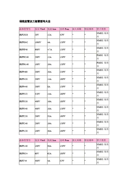
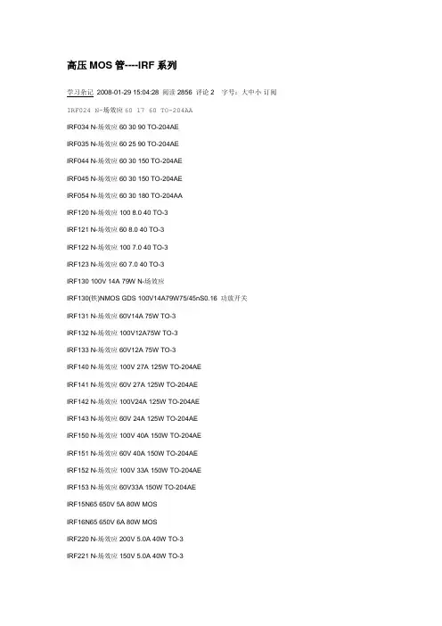
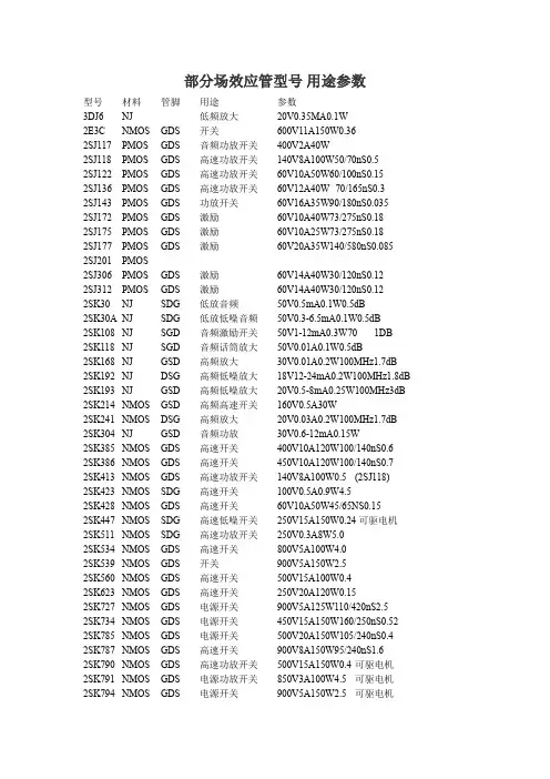
IRF830A
- 格式:pdf
- 大小:141.49 KB
- 文档页数:8
www.irf.com13/20/03
IRF830ASMPS MOSFET
HEXFET® Power MOSFETlSwitch Mode Power Supply ( SMPS )lUninterruptable Power Supply
lHigh speed power switching
Benefits
Applications
lLow Gate Charge Qg results in Simple Drive RequirementlImproved Gate, Avalanche and dynamic dv/dt RuggednesslFully Characterized Capacitance and Avalanche Voltage and CurrentlEffective Coss specified ( See AN 1001)
VDSSRds(on) maxID
500V1.40Ω5.0A
Typical SMPS Topologies:l Two transistor Forwardl Half Bridge and Full Bridge
ParameterMax.UnitsID @ TC = 25°CContinuous Drain Current, VGS @ 10V5.0ID @ TC = 100°CContinuous Drain Current, VGS @ 10V3.2AIDMPulsed Drain Current 20PD @TC = 25°CPower Dissipation74WLinear Derating Factor0.59W/°CVGSGate-to-Source Voltage ± 30Vdv/dtPeak Diode Recovery dv/dt 5.3V/nsTJOperating Junction and-55 to + 150TSTGStorage Temperature RangeSoldering Temperature, for 10 seconds300 (1.6mm from case )°C
Mounting torqe, 6-32 or M3 screw 10 lbf•in (1.1N•m)
Absolute Maximum RatingsTO-220ABSDG
PD- 91878D
Notes through are on page 8IRF830A
2www.irf.comParameterMin.Typ.Max.Units ConditionsgfsForward Transconductance2.8––––––SVDS = 50V, ID = 3.0AQgTotal Gate Charge–––––– 24 ID = 5.0A
QgsGate-to-Source Charge––––––6.3nCVDS = 400VQgdGate-to-Drain ("Miller") Charge––––––11VGS = 10V, See Fig. 6 and 13 td(on)Turn-On Delay Time–––10–––VDD = 250VtrRise Time–––21–––ID = 5.0Atd(off)Turn-Off Delay Time–––21–––RG = 14Ω
tfFall Time–––15–––RD = 49Ω,See Fig. 10 CissInput Capacitance–––620–––VGS = 0VCossOutput Capacitance–––93–––VDS = 25VCrssReverse Transfer Capacitance–––4.3–––pFƒ = 1.0MHz, See Fig. 5CossOutput Capacitance–––886–––VGS = 0V, VDS = 1.0V, ƒ = 1.0MHz
CossOutput Capacitance–––27–––VGS = 0V, VDS = 400V, ƒ = 1.0MHzCoss eff.Effective Output Capacitance–––39–––VGS = 0V, VDS = 0V to 400V
Dynamic @ TJ = 25°C (unless otherwise specified)ns
ParameterTyp.Max.UnitsEASSingle Pulse Avalanche Energy–––230mJIARAvalanche Current–––5.0AEARRepetitive Avalanche Energy–––7.4mJ
Avalanche Characteristics
SDG
ParameterMin.Typ.Max.Units ConditionsISContinuous Source CurrentMOSFET symbol(Body Diode)––––––showing theISM
Pulsed Source Currentintegral reverse
(Body Diode) ––––––p-n junction diode.VSDDiode Forward Voltage––––––1.5VTJ = 25°C, IS = 5.0A, VGS = 0V trrReverse Recovery Time–––430650nsTJ = 25°C, IF = 5.0AQrrReverse RecoveryCharge–––1.622.4µCdi/dt = 100A/µs tonForward Turn-On TimeIntrinsic turn-on time is negligible (turn-on is dominated by LS+LD)
Diode Characteristics5.020A
ParameterTyp.Max.UnitsRθJCJunction-to-Case–––1.7RθCSCase-to-Sink, Flat, Greased Surface0.50–––°C/WRθJAJunction-to-Ambient–––62
Thermal Resistance
Static @ TJ = 25°C (unless otherwise specified)ParameterMin.Typ.Max.Units ConditionsV(BR)DSSDrain-to-Source Breakdown Voltage500––––––VVGS = 0V, ID = 250µA∆V(BR)DSS/∆TJ
Breakdown Voltage Temp. Coefficient ––– 0.60 ––– V/°C Reference to 25°C, ID = 1mA
RDS(on)Static Drain-to-Source On-Resistance––––––1.4ΩVGS = 10V, ID = 3.0A VGS(th)Gate Threshold Voltage2.0–––4.5VVDS = VGS, ID = 250µA––––––25µAVDS = 500V, VGS = 0V––––––250VDS = 400V, VGS = 0V, TJ = 125°CGate-to-Source Forward Leakage––––––100VGS = 30VGate-to-Source Reverse Leakage––––––-100nAVGS = -30V
IGSS
IDSSDrain-to-Source Leakage CurrentIRF830A
www.irf.com3Fig 4. Normalized On-ResistanceVs. Temperature
Fig 2. Typical Output CharacteristicsFig 1. Typical Output CharacteristicsFig 3. Typical Transfer Characteristics0.010.1 1 10 1000.1 1 10 10020µs PULSE WIDTHT = 25CJ
°
TOPBOTTOMVGS15V10V8.0V7.0V6.0V5.5V5.0V4.5V
V , Drain-to-Source Voltage (V)I , Drain-to-Source Cur
r
ent (A)
DSD4.5V0.1
1
10 100
1 10 10020µs PULSE WIDTHT = 150CJ
°
TOPBOTTOMVGS15V10V8.0V7.0V6.0V5.5V5.0V4.5V
V , Drain-to-Source Voltage (V)I , Drain-to-Source Cur
r
ent (A)
DSD4.5V
0.1 1 10 1004.05.06.07.08.0V = 50V20µs PULSE WIDTHDS
V , Gate-to-Source Voltage (V)
I , Drain-to-Source Current (A)
GSDT = 25 CJ°
T = 150 CJ°
-60-40-200204060801001201401600.00.51.01.5
2.02.5
T , Junction Temperature( C)R , Drain-to-Source On Resistance
(Normalized)
JDS(on)°V=I=GSD10V
5.0A