Properties of Nanostractured Solar Cell Prepared at Different Etching Time
- 格式:pdf
- 大小:278.95 KB
- 文档页数:5
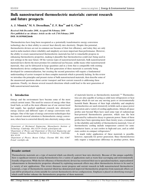
Bulk nanostructured thermoelectric materials:current research and future prospectsA.J.Minnich,a M.S.Dresselhaus,b Z.F.Ren *c and G.Chen *aReceived 16th December 2008,Accepted 5th February 2009First published as an Advance Article on the web 27th February 2009DOI:10.1039/b822664bThermoelectrics have long been recognized as a potentially transformative energy conversion technology due to their ability to convert heat directly into electricity.Despite this potential,thermoelectric devices are not in common use because of their low efficiency,and today they are only used in niche markets where reliability and simplicity are more important than performance.However,the ability to create nanostructured thermoelectric materials has led to remarkable progress inenhancing thermoelectric properties,making it plausible that thermoelectrics could start being used in new settings in the near future.Of the various types of nanostructured materials,bulk nanostructured materials have shown the most promise for commercial use because,unlike many other nanostructured materials,they can be fabricated in large quantities and in a form that is compatible with existing thermoelectric device configurations.The first generation of these materials is currently being developed for commercialization,but creating the second generation will require a fundamentalunderstanding of carrier transport in these complex materials which is presently lacking.In this review we introduce the principles and present status of bulk nanostructured materials,then describe some of the unanswered questions about carrier transport and how current research is addressing these questions.Finally,we discuss several research directions which could lead to the next generation of bulk nanostructured materials.I.IntroductionEnergy and the environment have become some of the most critical current issues.The need for sources of energy other than fossil fuels,as well as the most efficient use of our current fossil fuel supply,has sparked significant research into alternative energy sources and different types of energy conversion tech-nologies.One of the types of energy conversion technologies that has received renewed attention is thermoelectric energy conver-sion,where heat is converted directly into electricity using a classof materials known as thermoelectric materials.1–6Thermoelec-trics are also capable of acting as solid state refrigerators or heat pumps which do not use any moving parts or environmentally harmful fluids.Because of their high reliability and simplicity thermoelectrics are used extensively in fields such as space power generation and a variety of cooling applications.Almost all space probes sent beyond Mars have used some type of radioisotope heat-powered thermoelectric generator,which uses the heat generated by radioactive decay to generate power.Some of these probes have been operating more than twenty years,a testament to the reliability and stability of thermoelectric es of thermoelectric cooling include temperature control for semi-conductor lasers,as seat coolers in high-end cars,and as solid-state coolers in compact refrigerators.7A much wider application of these materials is possible,however,especially for power generation.Since thermoelectrics only require a temperature difference to produce power,theseaDepartment of Mechanical Engineering,Massachusetts Institute of Technology,Cambridge,MA,02139.E-mail:gchen2@ bDepartment of Physics and Department of Electrical Engineering and Computer Science,Massachusetts Institute of Technology,Cambridge,MA,02139cDepartment of Physics,Boston College,Chestnut Hill,MA,02467.E-mail:renzh@REVIEW /ees |Energy &Environmental Sciencematerials can easily extract energy from waste heat streams or other low-grade sources of energy.One example application currently under study is using thermoelectrics to extract elec-tricity from the hot exhaust stream of cars,8a very attractive application for automakers as consumers are increasingly inter-ested in cars with higher gas mileage.Another interesting application uses thermoelectrics to enhance the combustion efficiency of wood stoves used in developing countries, decreasing smoke output and reducing the amount of wood needed to cook.9Thermoelectrics are also able to generate power from the sun by using solar energy to create a temperature difference across a thermoelectric material;this is known as solar thermal energy conversion.10–13Given the applications just described,it is clear that there is a large potential market for thermoelectrics far beyond the few applications discussed here.However,today thermoelectric devices are not in common use.This is partly because they have a low efficiency relative to mechanical cycles,and partly because there are engineering challenges related to using ther-moelectric devices for general applications.7Thus economic and engineering considerations currently restrict the use of thermoelectrics.This could soon change.The thermoelectricsfield has seen remarkable progress in improving thermoelectric properties due to the recently gained ability to create nanostructured materials such as superlattices,14quantum dots,15nanowires,16,17and nanocomposites.18–21By exploiting nanoscale effects,these materials are able to obtain enhancements in thermoelectric properties which cannot be achieved in traditional bulk mate-rials,resulting in large increases in the thermoelectricfigure of merit,14–18,22which is traditionally denoted by ZT and will be further discussed in the next section.Some enhancements in the figure of merit ZT made in recent years are shown in Fig.1. Many different material systems exhibit enhancedfigures of merit,and most have broken the ZT z1barrier which was the maximum ZT of any material for overfifty years.It should also be mentioned that there are several efforts currently under way to solve engineering challenges related to creating thermoelectric devices,although that is not the focus of this review.7 Although a high ZT has been reported in nanostructured materials such as superlattices,quantum dots,and nanowires, many of these materials are not practical for large-scale commercial use because they are fabricated by atomic layer deposition processes such as molecular beam epitaxy,making Austin Minnich is a PhD candi-date in the Department ofMechanical Engineering at theMassachusetts Institute ofTechnology.His research inter-ests focus on modeling of trans-port processes in nanocompositethermoelectric materials andexperimental characterizationofthermoelectrics.Dr Mildred Dresselhaus,anInstitute Professor of electricalengineering and physics at theMassachusetts Institute ofTechnology,started work on lowdimensional thermoelectricityaround1990as a new approachto enhance the thermoelectricfigure of merit.She also headedup a DOE/BES study on BasicResearch Needs for theHydrogen Economy and servedas Director for the Office ofScience of the DOE during thelast year of the Clinton Admin-istration.Dr Z. F.Ren,professor ofphysics at Boston College,specializes in high performancethermoelectric materials andsolar thermoelectric systems,solar photovoltaic systems,mechanics of nanotubes/nano-wires and nanocomposites,water splitting and purification,bio agent delivery,and biosensors.Dr Gang Chen is currentlya professor at MassachusettsInstitute of Technology.Heobtained his PhD degree fromUC Berkeley in1993.He was anassistant professor at DukeUniversity from1993–1997,anassociate professor at Universityof California at Los Angelesfrom1997–2000,and moved toMIT in2000.He is a recipient ofthe NSF Young InvestigatorAward,a Guggenheim Fellow,the ASME Heat TransferMemorial Award,and theR&D100Award.He has pub-lished extensively in the area of nanoscale energy transport andconversion and nanoscale heat transfer.He currently serves on theeditorial boards for four journals in heat transfer and nanotech-nology and is the chair of ASME Nano Institute.them slow and expensive to fabricate and restricting the amount of material that can be produced.Another type of nano-structured material,known as a bulk nanostructured material,is a material which is fabricated using a bulk process rather than a nanofabrication process,and has the important advantage of being able to be produced in large quantities and in a form that is compatible with commercially available devices.Thus far,of all the nanostructured materials only bulk nanostructured materials have been produced in enough quantity to be used in this manner;superlattice or quantum dot structures are currently only able to be produced as thinfilms.This practicality is a key reason why there is significant interest in bulk nanostructured materials and optimism that they can be used in a commercial setting.Indeed,efforts to commercialize thefirst generation of these materials are ongoing.Nanostructured materials and thermoelectrics have been the subject of significant research in recent years and there are many reviews available.6,7,27,28Interested readers are encouraged to look at these additional references for more detail about the topics discussed here.Instead of doing a detailed review,we focus on discussing challenges in creating the next generation of bulk nanostructured materials,which will require both a higher level of control in producing bulk nanostructures and a fundamental understanding of carrier transport processes in these complex materials.The organization of the review is as follows.First,we discuss the principles of thermoelectric energy conversion and introduce the concept of bulk nanostructured materials,along with some of the details of their properties and fabrication methods.We then describe the challenges in understanding carrier transport in these materials and review the current research focused on addressing these challenges.Finally,we identify strategies and research directions which could lead to the next generation of bulk nanostructured thermoelectric materials.II.Principles of thermoelectric energy conversion Thermoelectric materials are capable of converting heat directly into electricity.They are based on the Seebeck effect,discovered by Thomas Johann Seebeck in1821.Seebeck showed that a compass needle is deflected when a temperature gradient is imposed on two different metals electrically connected in a closed loop;the deflec-tion of the compass needle was later realized to be caused by the generation of a magneticfield due to an electrical current in the loop.The phenomenon of an electrical current induced by a temperature gradient was termed‘‘thermoelectricity.’’Today we have a physical explanation for this phenomenon: mobile charge carriers(electrons or holes)at the hot side of the material have more thermal energy than carriers at the cold side,causing a net diffusion of mobile carriers to the cold side. Since there are more mobile carriers at the cold side than the hot side,the inhomogeneous charge distribution forms an electricfield which opposes the diffusion.If the material is in an open circuit,equilibrium will be reached when the rate at which carriers move from the hot side to the cold side due to diffusion is balanced by the rate at which carriers move from the cold side to the hot side due to the electricfield.Thus in equilibrium an electrochemical potential will form in response to a temper-ature gradient;this electrochemical potential is known as the Seebeck voltage,and the amount of voltage generated per unit temperature gradient is called the Seebeck coefficient.If the material is connected to a circuit,the electrochemical potential will drive a current which can be used to perform electrical work,which is the basis for thermoelectric power generation.1,2 This is illustrated in Fig.2(a).In Seebeck’s case,the tempera-ture gradient-induced electrochemical potential created a current in the circuit,which in turn generated a magneticfield which deflected the compass needle.A typical thermoelectric device is shown in Fig.2(b).Modern devices consist of many legs of alternating n-type and p-type materials,allowing a current toflow through each leg sequen-tially while heatflows through each leg in parallel.For power generation applications,modules are subjected to atemperature Fig.2(a)Schematic of thermoelectric power generation;(b)a typical thermoelectric device;and(c)an example demonstration of thermoelectric powergeneration.Fig.1Figure of merit ZT of current state of the art thermoelectricmaterials versus temperature.The dashed lines show the maximum ZTvalues for bulk state of the art materials,and the solid lines show recentlyreported ZT values,many of which were obtained in bulk nanostructuredmaterials.(BiSbTe,Ref.[18];Na0.95Pb20SbTe22,Ref.[23];PbTe/PbS,Ref.[24];Pb0.98Tl0.02Te,Ref.[25];Pb1+x Sb y Te,Ref.[26];n-SiGe,Ref.[20];p-SiGe,Ref.[21]).gradient over the length of the legs and connected to a circuit,as in Fig.2(c).Here a commercial thermoelectric module is sub-jected to a temperature difference using aflame as a heat source and a large aluminum block as the cold side heat sink.The imposed temperature gradient creates an electrochemical potential difference between the hot side and the cold side of the thermoelectric material which drives a current around the circuit, lighting up the LEDs.Thermoelectrics can also be used as solid-state refrigerators or heat pumps by driving a current in a circuit with two dissimilar materials.This mode exploits the Peltier effect, discovered by Jean-Charles Peltier in1834,where heat is absorbed or rejected at the interface of two dissimilar materials when a current is injected around a circuit.This is explained by introducing the Peltier coefficient,which is a material dependent parameter that is related to the Seebeck coefficient and which describes how much thermal energy is carried per charge carrier.Since the heat current must be continuous across the interface of two materials,if the materials have different Peltier coefficients heat will be either rejected or absorbed at the interface,depending on the sign of the difference between the Peltier coefficients and the direction of the current.If the current is injected in one direction the junction will extract heat,1,2,29which is the basis for thermoelectric refrigeration;a current in the other direction will produce heat at the junc-tion,and the device is acting as a heat ually the two materials are chosen to be thermoelectric materials with the opposite majority carrier(one n-type leg and one p-type leg)to maximize the difference between the Peltier coefficients and hence the amount of heat absorbed or generated.III.Thermoelectric materialsMaterials which are able to efficiently generate power using the Seebeck effect or refrigerate using the Peltier effect are known as thermoelectric materials.We would like a way to determine whether a given material will be a good thermoelectric material based on its properties.We can make educated guesses as to which properties will be important based on intuition:since the material has to pass electrical current in both the power gener-ation and refrigeration mode we expect to need a material with high electrical conductivity.Since we want a large voltage to be generated per unit temperature gradient a large Seebeck coeffi-cient is important.Finally,as we need to be able to maintain a temperature difference across the material,it seems reasonable to look for materials that also have low thermal conductivity.A simple heat transfer analysis yields the dimensionless parameter we seek,which is denoted ZT:ZT¼S2sT(1)S is the Seebeck coefficient,which was defined earlier,s is the electrical conductivity,k is the thermal conductivity,and T is the absolute temperature at which the properties are measured.1,2 For a material to be an efficient thermoelectric material we want ZT as high as possible.This equation shows our initial guesses were correct:we desire materials with high electrical conduc-tivity,high Seebeck coefficient,and low thermal conductivity. Unfortunately,nature does not provide many materials with these properties.Metals have very high electrical conductivity but also very high thermal conductivity.Glasses are the opposite, having very low thermal conductivity but also very low electrical conductivity.The material which would have the best thermo-electric properties was termed a‘‘phonon glass,electron crystal,’’because it would have a low thermal conductivity,as in a glass, but still conduct electricity,as in a well-ordered crystal.30After much experimentation,it was eventually determined that alloyed semiconductors with high carrier concentration are the most efficient bulk thermoelectric materials.31The high carrier concentration allows for a good electrical conductivity,and the electrical properties can be optimized by varying the carrier concentration.Alloying disrupts the transport of phonons (quantized lattice vibrations which carry heat),resulting in a reduced thermal conductivity.The lattice thermal conductivity can be further reduced by using heavy elements with low sound velocities,such as Bi,Te,and Pb.Examples of commercial thermoelectric materials are Bi2Te3and alloys such as Bi x Sb2Àx Te3at room temperature,PbTe and alloys such as PbTe–PbSe at moderate temperature,and the alloy Si80Ge20at high temperature.Despite having multiple parameters to adjust,optimizing all the parameters together turns out to be very difficult because the properties are interdependent.For example,if wefind the elec-trical conductivity is too low,we might want to increase the carrier concentration.However,while increasing the carrier concentration will increase the electrical conductivity,it will also decrease the Seebeck coefficient and increase the electronic contribution to the thermal conductivity.From Eqn1,we see that these changes in properties will most likely not lead to a net increase in ZT,since any favorable change in one property is accompanied by an unfavorable change in the other properties. These conflicting trends are illustrated in Fig.3for n-type Si80Ge20.This type of dilemma caused the maximum ZT of any thermoelectric material to remain at ZT z1for almostfiftyyears.Fig.3Normalized thermoelectric properties and ZT versus doping concentration at300K for n-type Si80Ge20.Curves are calculated from a numerical model developed by the authors.In thefigure k refers to thermal conductivity,S refers to the Seebeck coefficient,and s refers to the electrical conductivity.IV.Nanostructured materialsThere have been two primary approaches taken to overcome these challenges.The first approach focuses on creating new materials:researchers try to synthesize complex solid solutions which have the desired properties.These materials have very complex crystal structures which can exhibit a low lattice thermal conductivity.An excellent review on this approach was recently published.27The other approach,which is the focus of this review,is to create nanostructured materials.By using the same materials but in a nanostructured form,it is possible to modify thermoelectric properties in ways that are not possible with bulk materials,which can lead to an enhancement in ZT.6,18,22,32–34The idea of selectively modifying material properties using lower dimensional structures was introduced by Hicks and Dresselhaus in 1993.22They theoretically showed that by using two-,one-,or even zero-dimensional structures one could obtain significant increases in electronic properties,far beyond what was believed possible in bulk materials.Others later theoretically showed a significant reduction in lattice thermal conductivity is possible by using nanostructures.33,34Stimulated by these predictions,researchers were able to fabricate nanostructures such as superlattices (2D structures),nanowires (1D structures),and quantum dots (0D structures),forming thin-film materials for which thermoelectric properties could be measured.Soon thereafter,high ZTs were reported in a thin-film superlattice 14and a quantum dot superlattice.15Silicon nanowires were also reported to have a high ZT.16,17All of these materials exhibited a decrease in lattice thermal conductivity.Others have reported that another type of nanostructure consisting of In 0.53Ga 0.47As with embedded ErAs nanoparticles can have a very low thermal conductivity below that of the corresponding bulk alloy.35These researchers have also tried to use these particles to increase the Seebeck coefficient by filtering out low energy electrons,36but a net increase in ZT from this method has not been confirmed.These reports of enhanced ZT on thin film structures and nanowires have demonstrated the principle of nanostructuring to enhance ZT,although questions linger regarding the accuracy of the ZT reported due to experimental difficulties in measuring the properties accurately.However,even if these results can be confirmed,materials fabricated by atomic layer deposition techniques are not easily incorporated into commercial devices because they are slow and expensive to fabricate,and they cannot be fabricated in sufficient quantities.Fortunately,theoretical results obtained from studying superlattices provided a solutionto this dilemma.Modeling of phonon transport in superlattices indicated that the primary benefit from nanostructures,a reduced lattice thermal conductivity,does not require an atomically perfect interface or an exact geometry.34All that is required is a material with a high density of interfaces,which can be present in any geometry.37This discovery led to the idea of a nanocomposite,which retains the high density of interfaces but does not have a special geometry or structure,significantly simplifying the fabrication process and allowing the material to be produced in large quantities.38A nanocomposite is thus a type of bulk nanostructured material and will be the focus of this review.V.NanocompositesA.ConceptThe term ‘‘nanocomposite’’has been used to describe several different types of structures.The original concept was for either nanoparticles embedded in a host or a heterostructure geometry with nanoparticles of different materials adjacent to each other.38,39For the heterostructure geometry,when the two materials are the same the nanocomposite is essentially a mate-rial with nanometer sized grains.A TEM image of a typical Si 80Ge 20nanocomposite 20is shown in Fig.4.From the scale bars we can see that the grain size is only ten or twenty nanometers,much smaller than a typical Si 80Ge 20grain size of one micron and larger.40–42Because these nanostructures have a size smaller than the phonon mean free path but greater than the electron or hole mean free path,phonons are more strongly scattered by the interfaces than are electrons or holes,resulting in a net increase in ZT.As might be expected,because nanocomposites are not formed by atomic layer deposition methods,they are significantly quicker and cheaper to fabricate than superlattices or other nanostructures,yet retain the same enhancements in thermo-electric properties.The nanocomposite concept has been vali-dated in several material systems:an increase in ZT for n-type Si 80Ge 20,20p-type Si 80Ge 20,21and p-type Bi x Sb 2Àx Te 318,19has been experimentally demonstrated.Perhaps more importantly,the Bi x Sb 2Àx Te 3nanocomposite was able to be incorporated into a macroscale device with record performance.18B.FabricationWhen the nanocomposite concept was still being developed,nanostructured materials which exhibited enhanced thermo-electric properties had only been created using atomic layer deposition techniques,and it was unclear whether any bulk process could create a thermodynamically stable,nanostructured material with an improved figure of merit.The first challenge is to create a material with nanoscale structures throughout using only a bulk process.While several techniques are available to create nanoparticles,43,44combining the nanoparticles into a fully dense solid is not as straightforward.Once the bulk material has been fabricated,the next challenge is to adjust the fabrication conditions so that the figure of merit is improved.This is more difficult because the effects of the fabrication conditions on the nanostructures formed and the material’s thermoelectric prop-erties are not always clear.A still unresolved question is whyFig.4(a)TEM and (b)HRTEM images of a Si 80Ge 20nanocomposite (from Ref.[20]).certain nanostructured materials exhibit improved properties while others do not.Some fabrication methods,while capable of creating a nanostructured material,cannot produce a material with an improved ZT no matter how the fabrication conditions are adjusted.Thefinal challenge is to produce a thermodynamically stable material which can retain its nanoscale structures while being used in a practical device.If the nanostructures spontaneously dissolve during the course of operation the thermoelectric properties will return to those of the bulk material,removing any increase in efficiency that the nanostructured material was supposed to give.Creating a thermodynamically stable nano-structured material is difficult because the nanostructured form is not an equilibrium state of the material.Diffusion and energies associated with interfaces often act to remove nanoscale struc-tures or variations in composition;in PbTe,for example,nano-sized grains are not stable at elevated temperatures due to their high surface energy.Since in practice thermoelectrics must operate for years at high temperatures to maximize thermody-namic efficiency,thermal stability of nanostructured materials is an important issue and is a topic of ongoing research.Despite these difficulties,several bulk processes have been developed in recent years which have successfully created stable nanocomposites with improved properties over those of their bulk counterparts.One method uses ball milling and hot pressing to create nanograined materials.In this technique,raw compo-nent elements,such as Bi and Te or Si and Ge,are ground into a nano-particle dust using a ball milling machine.The resulting mixture is then hot pressed at an appropriate temperature and pressure.If the pressing temperature and duration are adjusted correctly,the nanoparticles will fuse together but leave the interface between each particle intact,creating a fully dense solid material with nanosize grains,as shown in Fig.4.This technique has been successfully implemented on n-type Si80Ge20,20p-type Si80Ge20,21and different types of Bi x Sb2Àx Te3.18,19The advan-tages of this method are that it is simple and inexpensive to fabricate the materials,and the technique can be applied to any material system.Another method to create a bulk nanocomposite is to use thermal processing techniques to induce the formation of nanoscale precipitates,an approach which has been successfully used by the Kanatzidis group in several material systems.23,24,45,46 By choosing the appropriate compounds and subjecting the material to a thermal processing procedure,a metastable solid solution of different elements can be made to undergo spinodal decomposition or nucleation and growth mechanisms to create nanoscale features.24A related technique,known as matrix encapsulation,uses the fact that some materials are soluble in others in the liquid state but not in the solid state.By rapidly cooling the liquid mixture,the insoluble minority phase will precipitate,forming nanoparticles embedded in the host phase.45 These techniques have been applied with considerable success to several different solid solutions.High ZTs have been reported in n-type AgPbTe2/PbTe,46n-type Pb1Àx Sn x Te/PbS,24and p-type Na1Àx Pb m Sb y Te m+2.23All of these materials achieved their high ZT values by exhibiting a markedly reduced thermal conduc-tivity.To give an idea of the magnitude of the reduction,bulk PbTe has a thermal conductivity of about2.4W mÀ1KÀ1at300 K,while PbTe with two percent Sb that is matrix encapsulated has a thermal conductivity of about0.8W mÀ1KÀ1,a remarkable decrease.VI.Challenges in understanding carrier transport Nanocomposites have been successful in increasing ZT by reducing the thermal conductivity below that of the bulk material while allowing for large scale,quick,and inexpensive fabrication. Thefirst generation of nanocomposites has been developed,and efforts to use the materials in commercial devices are currently under way.However,as discussed in the introduction,devel-oping the second generation of nanocomposites will require a more controlled design process where the thermoelectric properties of different nanostructures can be predicted and the desired structure created using a bulk procedure.The current design process of trial and error will not be sufficient.This goal can only be achieved with a fundamental understanding of transport in these complex materials and how their nanoscale structure affects bulk properties.In the next section we discuss the difficulties in analyzing carrier transport in nanocomposites and what research is taking place to address these difficulties.While most of our discussion is focused on scattering processes caused by grain boundaries,it is important to note that as the grains become smaller and smaller the volume fraction of grain boundaries becomes comparable to the volume fraction of the material itself,making the grain boundaries essentially another phase inside a host material.The properties of the overall material are determined not just by scattering processes but by the presence of the grain boundary phase.Since the properties and composition of the grain boundary are almost completely unknown and not easily deter-mined,transport in nanocomposites is usually explained in terms of grain boundary scattering processes,which is the approach we will follow.This dilemma already illustrates how much is unknown about carrier transport in nanocomposites.A.Phonon transportSince most nanocomposites to date have achieved their high ZT values by a reduction in lattice thermal conductivity(in this section just termed‘‘thermal conductivity’’),one might expect that phonon transport in nanocomposites is fairly well under-stood.However,the situation turns out to be just the opposite. Even in bulk materials,there is much uncertainty regarding the values of key quantities such as the phonon mean free path. Furthermore,the precise way in which interfaces affect phonon transport to reduce thermal conductivity in nanocomposites remains poorly understood.Theoretical predictions for the lower limit of thermal conductivity in nanostructured materials also turn out to be wrong,as was experimentally demonstrated by Cahill.47This physical understanding is crucial to further reducing the thermal conductivity,however,and so here we highlight what is known about phonon transport and what we seek to understand.First,let us discuss what is known.Nanocomposites have shown that they are able to achieve a thermal conductivity lower than that of their bulk counterparts.Before the creation of nanostructured materials it was believed that the lower limit to the thermal conductivity was set by the value obtained by an。

纳米结构材料及其技术在太阳能电池中的应用和发展现状王二垒,张秀霞,杨小聪,张绍慧(北方民族大学电信学院,宁夏银川750021)摘要:太阳能电池的发展和利用离不开太阳能电池材料和技术的发展,文中对纳米结构材料及其技术在太阳能电池和太阳能光电转化技术中的应用和发展现状做了简要综述。
介绍了多元化合物太阳电池纳米材料、染料敏化太阳电池纳米材料和有机聚合物太阳电池结构纳米材料的研究现状和技术创新,并指出其发展趋势。
关键词:太阳能电池;阳能电池材料;纳米结构材料;光电转化中图分类号:O 484.4文献标识码:A文章编号:1674-6236(2012)24-0184-04Application and development of NANO -structured materials andtechnologies for solar cellsWANG Er -lei ,ZHANG Xiu -xia ,YANG Xiao -cong ,ZHANG Shao -hui(School of Electronics and Information Engineering ,North National University ,Yinchuan 750021,China )Abstract:The development and use of solar cells can not be separated from the development of solar materials and technologies ,this paper summarized the application and development of NANO -structured material and technologies for solar cells and solar photoelectric conversion.The study status and technology innovation for multi -element compounds solar cells of NANO -structured materials ,dye -sensitized solar cells of NANO -structured materials and organic polymer solar cells of NANO -structured materials were introduced ,the development tendency were also been pointed out.Key words:solar cells ;solar cell material ;NANO -structured material ;photoelectric conversion收稿日期:2012-08-28稿件编号:201208157基金项目:国家自然科学基金资助项目(60844006);北方民族大学研究生创新项目(2012XYC040;2012XYC041);宁夏高等学校科学研究项目基金(2011JY002);北方民族大学科学研究专项任务项目基金(2011XJZKJ02);北方民族大学大学生创新项目(CJJ-CX-DX-40;CJJ-CX-DX-39)作者简介:王二垒(1985—),男,河南商水人,硕士研究生。

Lyso-Tracker Red (溶酶体红色荧光探针)产品简介:Lyso-Tracker Red 是一种溶酶体(lysosome)红色荧光探针,能通透细胞膜,可以用于活细胞溶酶体特异性荧光染色。
Lyso-Tracker Red 为采用Molecular Probes 公司的DND-99进行了荧光标记的带有弱碱性的荧光探针,其中仅弱碱可部分提供质子,以维持pH 在中性,可以选择性地滞留在偏酸性的溶酶体中,从而实现对于溶酶体的特异性荧光标记。
中性红(Neutral Red)和吖啶橙(Acridine Orange)也都可以对溶酶体进行荧光染色,但中性红和吖啶橙的染色缺乏特异性。
Lyso-Tracker Red 适用于活细胞溶酶体的荧光染色,但不适合用于固定细胞溶酶体的荧光染色。
Lyso-Tracker Red 分子的化学结构式参考图1。
图1. Lyso-Tracker Red 的化学结构式。
Lyso-Tracker Red 的分子式为C 20H 24BF 2N 5O ,分子量为399.25,最大激发波长为577nm ,最大发射波长为590nm 。
Lyso-Tracker Red 的激发光谱和发射光谱参考图2。
图2. Lyso-Tracker Red的激发光谱和发射光谱。
Lyso-Tracker Red 是嗜酸性荧光探针,用于活细胞内酸性细胞器的标记和示踪。
这些探针具有几个重要特征,包括高度选择靶向酸性细胞器和在纳摩尔浓度有效标记活细胞。
Lyso-Tracker Red 必须在极低浓度(通常约50nM)下才能获得优异的选择性。
这些探针的滞留(retention)机制虽然没有被研究清楚,但很可能与酸性细胞器的质子化和滞留性有关,Lyso-Tracker Red 探针的内吞作用动力学研究显示染料进入活细胞的摄入时间仅几秒即可。
然而,这些溶酶体探针会导致溶酶体被碱化,长期孵育会诱使溶酶体pH 值的增加。

DOI: 10.13822/ki.hxsj.2020007577j综述与进展化学试剂,2020,42(11) ,1309〜1317二茂铁染料在敏化太阳能电池的研究进展王磊、李耀龙2,陈瑜“(1.天津理工大学,化学化工学院,天津300384;2.天津大格科技有限公司,天津301700)摘要:染料敏化太阳能电池(DSSC)已成为低成本光伏最有前途的技术之一,也是作为基于传统太阳能电池的有前途的替代品,引起了相当大的研究兴趣。
目前为止,为制作高效率的染料敏化太阳能电池,许多研究学者制作出了各种各样的敏化剂。
染料敏化剂对光收集和电子注入效率都起着至关重要的作用。
染料敏化剂可分为两种:金属有机染料敏化剂和非金属染料敏化剂。
二茂铁或二茂铁衍生物可作为供电子基的有机染料敏化剂,可以提高太阳能电池的光电转化效率,受到越来越多的关注。
关键词:有机光伏;太阳能电池;染料敏化剂;二茂铁;光电转换效率中图分类号:062丨.3 文献标识码:A文章编号:0258-3283( 2020) 11 -丨309-09Progress of Ferrocene Dyes in Sensitized Solar Cells WANG Lei' ,L I Yao-long1 ?CHEN Y u*\ 1.School of Chemistry a n d C h e mical Engineering,Tianjin University of Te c h n o l o g y,Tianjin 300384,C h i n a;2.Tianjin D a g Technology C o.,Ltd.,Tianjin 301700, C h i n a) ,H u a x u e Shiji,2020,42(11) , 1309 ~ 1317Abstract:Dye-sensitized solar cells (D S S C)have b e c o m e one of the most promising technologies for low-cost photovoltaics,and as promising alternatives to traditional solar cells,have attracted considerable research interest.So f a r,m a n y researchers have prod u c e d a variety of sensitizers to produce highly efficient dye-sensitized solar cells.Dye sensitizers play a vital role in both light collection and electron injection efficiency.There are two types of dye sensitizers :metal-organic dye sensitizers and non-metallic or- ganic dye sensitizers.Ferrocene a n d ferrocene derivatives can be used as electron-donor-based organic dye sensitizers to improve the photoelectric conversion efficiency of solar cells,which is receiving increasing attention.Key w ords:organic photochemistry;solar cells;dye sensitizers;ferrocene;photoelectric conversion efficiency随着科技的进步和人民生活水平的逐渐提高,越来越多的人开始关注国家的能源发展问题,然而随之出现的能源和燃料的危机,使得人类社会需要寻找一种可以代替化石燃料的能源。

Solar CellIntroductionA solar cell, also known as a photovoltaic cell, is an electrical device that converts sunlight into electricity by the photovoltaic effect. It is a key component in solar panels and plays a crucial role in harnessing solar energy. Solar cells are widely used to generate clean and renewable energy for various applications including residential, commercial, and industrial sectors.Working PrincipleSolar cells are based on the principle of the photovoltaic effect. This effect occurs when certain materials, known as semiconductors, absorb photons from sunlight, which then excite the electrons within the material. The excited electrons create an electric current when they flow through the material. This current can be harnessed and used as a source of electrical energy.Types of Solar CellsThere are several types of solar cells that vary in their material composition and efficiency. The most common types include:1.Monocrystalline Silicon Solar Cells:–These solar cells are made from a single crystal structure, resulting in high efficiency.–They have a uniform dark color and are easily recognizable by their rounded edges.–Monocrystalline solar cells tend to be more expensive due to the manufacturing process.2.Polycrystalline (Multicrystalline) Silicon Solar Cells:–These solar cells are made from multiple crystal structures, which makes them less efficient compared to monocrystalline cells.–They have a bluish color and a granular appearance.–Polycrystalline solar cells are more cost-effective compared to monocrystalline cells.3.Thin-Film Solar Cells:–These solar cells are made by depositing a thin layer of semiconductor material onto a substrate.–Thin-film solar cells are flexible and lightweight, making them suitable for various applications.–They have a lower efficiency compared to crystalline silicon solar cells but are cheaper toproduce.anic Solar Cells:–Also known as organic photovoltaic cells (OPV), these solar cells use organic materials as thesemiconductor.–Organic solar cells have the advantage of being printable and can be manufactured using low-costprocesses.–However, their efficiency is currently lower compared to other types of solar cells.Manufacturing ProcessThe manufacturing process of solar cells involves several steps, including:1.Silicon Production:–The primary material used in most solar cells is silicon, which is obtained through a complex process.–Pure silicon is extracted from silica (SiO2), which is then refined and purified to reach the desiredlevel of purity.2.Wafer Production:–The purified silicon is transformed into solid blocks called ingots.–The ingots are then sliced into thin wafers using a diamond saw.–These wafers serve as the base for the solar cells.3.Doping:–Doping is a process in which impurities are added to the silicon wafer to create a p-n junction, which is necessary for the photovoltaic effect.–The addition of phosphorous or boron atoms introduces extra electrons or electron holes into the silicon structure, respectively.4.Formation of Layers:–Several layers are formed on the surface of the silicon wafer to enhance the solar cell’s efficiency.–These layers include anti-reflective coatings and metal contacts.5.Assembly into Modules:–The individual solar cells are interconnected and assembled into modules or panels.–The modules are then encapsulated to protect the solar cells from environmental factors.Efficiency and LimitationsThe efficiency of a solar cell refers to the percentage of sunlight converted into electrical energy. The efficiency varies depending on the type of solar cell and its manufacturing process. Currently, the most efficient solar cells on the market can achieve efficiencies of over 20%.Solar cells, however, have certain limitations, including:1.Efficiency Drop with Temperature:–Solar cells become less efficient as their temperature increases.–High temperatures can reduce the voltage and current output, lowering the overall performance.2.Dependency on Sunlight:–Solar cells rely on sunlight and their efficiency decreases in cloudy or shaded conditions.–The placement and orientation of solar panels play a crucial role in maximizing energy output.3.Cost:–The initial cost of solar cell production is relatively high, although it has been decreasing inrecent years.–The cost of solar cells is influenced by factors such as material type, manufacturing process, andmarket demand.ApplicationsSolar cells have a wide range of applications, including:1.Residential Solar Power Systems:–Solar panels installed on rooftops can generate electricity for residential use.–Excess energy can be fed back into the grid or stored in batteries for later use.mercial and Industrial Solar Power Systems:–Large-scale solar power plants generate electricity for commercial and industrial applications.–These systems can supply power to factories, offices, and other commercial buildings.3.Portable Solar Chargers:–Solar cells can be used to power handheld devices such as smartphones, tablets, and laptops.–Portable solar chargers provide a convenient and renewable source of energy for outdoor activities.4.Solar Lighting:–Solar cells are used in outdoor lighting systems, including streetlights, garden lights, and pathwaylights.–These systems eliminate the need fortraditional electrical wiring and reduce energyconsumption.5.Space Applications:–Solar cells are extensively used in spaceapplications such as satellites and spacecraft.–In space, solar cells provide the necessary power for various onboard systems and equipment.ConclusionSolar cells are vital components in the generation of clean and renewable energy. They utilize the photovoltaic effect to convert sunlight into electricity, making them an environmentally friendly alternative to traditional energy sources. With advancements in technology and decreasing costs, solar cells are becoming increasingly popular and are expected to play a significant role in meeting our future energy needs.。
纳米防晒霜英语作文两百字Nanotech Sunscreen: A Revolutionary Approach to Sun Protection.In the realm of sun protection, the advent of nanotechnology has heralded a groundbreaking advancement: nanoformulated sunscreens. These innovative products leverage the unique properties of nanoparticles to offer unparalleled efficacy and benefits that surpass conventional chemical and mineral sunscreens.Nanoformulated sunscreens utilize nanoparticles, particles with sizes ranging from 1 to 100 nanometers, as their active ingredients. These nanoparticles are typically composed of inorganic materials such as zinc oxide or titanium dioxide, which inherently possess UV-absorbing properties. By reducing the particle size to the nanoscale, these sunscreens achieve remarkable sun protection while addressing the drawbacks of traditional formulations.Enhanced Sun Protection:The diminutive size of nanoparticles enables them to interact with UV radiation more effectively than larger particles. This increased surface area enhances their UV-absorbing capacity, resulting in superior sun protection. Nanoscale particles can effectively scatter, absorb, and reflect both UVA and UVB rays, providing broad-spectrum protection against the full range of harmful solar radiation.Improved Transparency:Conventional sunscreens often leave an unsightly white cast on the skin, particularly when applied in sufficient quantities to achieve adequate protection. This unappealing effect arises from the larger particle size of these formulations, which can scatter visible light. In contrast, nanoscale particles are too small to interact significantly with visible light, rendering them virtually transparent. Nanoformulated sunscreens can therefore provide high levels of sun protection without compromising aesthetics.Reduced Chemical Penetration:Chemical sunscreens rely on organic compounds that penetrate the skin to absorb UV radiation. However, some of these chemicals have raised concerns about potentialtoxicity and skin irritation. Nanoparticles, on the other hand, are designed to remain on the skin's surface, forming a physical barrier that deflects UV rays. This minimized chemical penetration reduces the risk of adverse reactions and ensures the safety of nanoformulated sunscreens.Broader Applications:Nanoformulated sunscreens offer unique advantages for a wider range of applications. They can be incorporated into clothing, cosmetics, and other products that are not traditionally associated with sun protection. This versatility extends their utility to situations where traditional sunscreen use is impractical or ineffective.In conclusion, nanoformulated sunscreens represent asignificant advancement in sun protection technology. Their enhanced efficacy, improved transparency, reduced chemical penetration, and broader applications make them a highly effective and convenient solution for protecting skin from the harmful effects of solar radiation. As research continues, the potential of nanotechnology in the realm of sunscreens is bound to expand even further, providing even greater protection and benefits for years to come.。
太阳电池solar cell通常是指将太阳光能直接转换成电能的一种器件。
硅太阳电池silicon solar cell硅太阳电池是以硅为基体材料的太阳电池。
单晶硅太阳电池single crystalline silicon solar cell单晶硅太阳电池是以单晶硅为基体材料的太阳电池。
非晶硅太阳电池(a—si太阳电池)amorphous silicon solar cell用非晶硅材料及其合金制造的太阳电池称为非晶硅太阳电池,亦称无定形硅太阳电池,简称a—si太阳电池。
多晶硅太阳电池polycrystalline silicon solar cell多晶硅太阳电池是以多晶硅为基体材料的太阳电池。
聚光太阳电池组件photovoltaic concentrator module?系指组成聚光太阳电池,方阵的中间组合体,由聚光器、太阳电池、散热器、互连引线和壳体等组成。
电池温度cell temperature系指太阳电池中P-n结的温度。
太阳电池组件表面温度solar cell module surface temperature系指太阳电池组件背表面的温度。
大气质量(AM)Air Mass (AM)直射阳光光束透过大气层所通过的路程,以直射太阳光束从天顶到达海平面所通过的路程的倍数来表示。
太阳高度角solar太阳高度角solar elevation angle太阳光线与观测点处水平面的夹角,称为该观测点的太阳高度角。
辐照度irradiance系指照射到单位表面积上的辐射功率(W/m2)。
总辐照(总的太阳辐照)total irradiation (total insolation)在一段规定的时间内,(根据具体情况而定为每小时,每天、每周、每月、每年)照射到某个倾斜表面的单位面积上的太阳辐照。
直射辐照度direct irradiance照射到单位面积上的,来自太阳圆盘及其周围对照射点所张的圆锥半顶角为8o的天空辐射功率。
The Properties of Carbon Nanotubes andGrapheneCarbon nanotubes (CNTs) and graphene are two of the most fascinating materials in the world of science and engineering. Both are made of carbon atoms, but they have unique properties that make them useful for a variety of applications in fields such as electronics, medicine, and materials science. In this article, we will explore the properties of CNTs and graphene in detail.StructureCarbon nanotubes are made of a single layer of graphene, which is a two-dimensional sheet of carbon atoms arranged in a hexagonal lattice. However, this sheet is rolled up into a tube, giving the CNT its distinctive cylindrical shape. CNTs can be single-walled or multi-walled, depending on the number of graphene layers that make up the tube.Graphene, on the other hand, is a flat sheet of carbon atoms that is only one atom thick. This makes graphene the thinnest material in the world, but it is also incredibly strong because of its tightly-packed hexagonal lattice structure. Graphene can be produced in large sheets through a process called chemical vapor deposition (CVD).Electrical PropertiesOne of the most important properties of CNTs and graphene is their electrical conductivity. Both materials are excellent conductors of electricity, with graphene being one of the best known conductors in the world.Graphene has a unique band structure that allows electrons to move freely through the material without any resistance, making it a perfect candidate for electronic devices such as transistors, sensors, and solar cells. CNTs also have high electrical conductivity, but their properties depend on their diameter, chirality (twist), and the number of graphene layers that make up the tube.Mechanical PropertiesWhile both CNTs and graphene are strong materials, they have different mechanical properties due to their unique structures. CNTs are some of the strongest materials in the world, with tensile strengths that are many times greater than that of steel. This is because CNTs have a strong covalent bond between carbon atoms that gives them exceptional stability.Graphene, on the other hand, is not as strong as CNTs, but it has excellent flexibility and elasticity. Because it is only one atom thick, graphene can be stretched and bent without losing its structural integrity. This makes it useful in applications such as membranes, where a thin, flexible but strong material is necessary.Thermal PropertiesAnother important property of both CNTs and graphene is their thermal conductivity. Both materials have high thermal conductivity, meaning they can transfer heat very efficiently. This makes them useful in applications such as thermal management, where they can be used as heat sinks or as filler materials in thermal interface materials.ApplicationsBecause of their unique properties, CNTs and graphene have numerous applications in a variety of fields. Some of these applications include:Electronics: Both CNTs and graphene have high electrical conductivity and can be used in electronic devices such as transistors, displays, and sensors.Medicine: Graphene and CNTs have potential applications in drug delivery, biomedical imaging, and tissue engineering.Materials science: CNTs and graphene can be used as fillers or reinforcements in composite materials, or as membranes in water purification and desalination.Energy: Graphene and CNTs have potential applications in energy storage and conversion, such as in batteries and fuel cells.ConclusionIn conclusion, CNTs and graphene are fascinating materials with unique properties that make them useful in a variety of applications. From electronics to medicine, materials science, and energy, these materials have the potential to revolutionize numerous industries. As researchers continue to explore their properties and develop new applications, the possibilities for CNTs and graphene are seemingly endless.。