可焊性wetting balance-资料
- 格式:ppt
- 大小:6.70 MB
- 文档页数:15
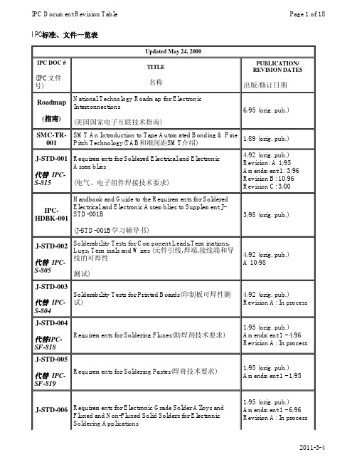
IPC标准、文件一览表Updated May 24, 2000IPC DOC # (IPC文件号) TITLE名称PUBLICATION/REVISION DATES出版/修订日期Roadmap (指南)National Technology Roadmap for ElectronicInterconnections(美国国家电子互联技术指南)6/95 (orig. pub.)SMC-TR-001SMT An Introduction to Tape Automated Bonding & FinePitch Technology(TAB和细间距SMT介绍)1/89 (orig. pub.)J-STD-001代替IPC-S-815Requirements for Soldered Electrical and ElectronicAssemblies(电气、电子组件焊接技术要求)4/92 (orig. pub.)Revision: A 1/95Amendment 1: 3/96Revision B: 10/96Revision C: 3/00IPC-HDBK-001Handbook and Guide to the Requirements for SolderedElectrical and Electronic Assemblies to Supplement J-STD-001B(J-STD-001B学习辅导书)3/98 (orig. pub.)J-STD-002代替IPC-S-805Solderability Tests for Component Leads,Terminations,Lugs, Terminals and Wires (元件引线,焊端,接线端和导线的可焊性测试)4/92 (orig. pub.)A 10/98J-STD-003代替IPC-S-804Solderability Tests for Printed Boards(印制板可焊性测试)4/92 (orig. pub.)Revision A: In processJ-STD-004代替IPC-SF-818Requirements for Soldering Fluxes(助焊剂技术要求)1/95 (orig. pub.)Amendment 1 - 4/96Revision A: In processJ-STD-005代替IPC-SF-819Requirements for Soldering Pastes(焊膏技术要求)1/95 (orig. pub.)Amendment 1 - 1/95J-STD-006Requirements for Electronic Grade Solder Alloys and Fluxed and Non-Fluxed Solid Solders for ElectronicSoldering Applications 1/95 (orig. pub.) Amendment 1 - 6/96 Revision A: In process(电子级固态焊料技术要求)J-STD-012Implementation of Flip Chip and Chip Scale Technology(FC和CSP器件的安装)1/96 (orig. pub.)J-STD-013Implementation of Ball Grid Array and Other HighDensity Technology(BGA和HDI器件的安装)7/96 (orig. pub.)IPC-DRM-18Component Identification Desk Reference Manual(元器件封装辨认手册)9/95 (orig. pub.)Revision A: 4/96Revision B: 2/97Revision C: 7/98J-STD-020Moisture/Reflow Sensitivity Classification of PlasticSurface Mount Devices(塑封表面器件对潮湿和再流焊的敏感度要求)October 1996 (orig.pub.)Revision A: 3/99IPC-DRM-40Through-Hole Solder Joint Evaluation Desk Reference Manual(通孔引线焊点评估参考手册)IPC-DRM-SMT Surface Mount Solder Joint Evaluation Desk Reference Manual(表面组装焊点评估参考手册)8/98IPC-T-50Terms and Definitions Interconnecting and PackagingElectronic Circuits(电子电路互连及封装术语和定义)8/75 (orig. pub.)A - 8/76B - 6/80C - 3/85D - 11/88E - 7/92F - 6/96IPC-SC-60Post Solder Solvent Cleaning Handbook (焊后溶剂清洗手册)4/87 (orig. pub.)Revision A: In processIPC-SA-61Post-Solder Semi-Aqueous Cleaning Handbook(焊后半水清洗手册)7/95 (orig. pub.)IPC-AC-62Post Solder Aqueous Cleaning Handbook (焊后水清洗手册)12/86 (orig. pub.)IPC-CH-65Guidelines for Cleaning of Printed Boards and Assemblies(印制板及其组件清洗导则) 12/90 (orig. pub.) Revision A: In processIPC-CS-70Guidelines for Chemical Handling Safety in Printed Board Manufacturing(印制板制造化学处理安全准则)8/88 (orig. pub.)IPC-CM-78被IPC-SM-780替代Guidelines for Surface Mounting and InterconnectingChip Carriers11/83 (orig. pub.)C - 3/88IPC-MP-83IPC Policy on Metrication(IPC公制化导则) 8/85 (orig. pub.)IPC-PC-90General Requirements for Implementation of StatisticalProcess Control(实施SPC的总技术规范)10/90 (orig. pub.)IPC-QS-95General Requirements for Implementation of ISO 9000Quality Systems(实施ISO 9000质量体系的总技术规范)4/93 (orig. pub.)IPC-L-108被IPC-4101替代Specification for Thin Metal Clad Base Materials forMultilayer Printed Boards3/76 (orig. pub.)A 10/80B 6/90IPC-L-109被IPC-4101替代Specification for Resin Impregnated Fabric (Pregreg) forMultilayer Printed Boards3/76 (orig. pub.)A 10/80B 7/92IPC-L-110 (已作废)Preimpregnated, B-Stage Epoxy-Glass Cloth forMultilayer Printed Cicuit BoardsAIPC-CC-110 被IPC-4121替代Guidelines for Selecting Core Constructions forMultilayer Printed Wiring Board Applications1/94 (orig. pub.)Revision A: 12/97IPC-L-112 被IPC-4101替代Specification for Composite Metal Clad Base materials forPrinted Boards7/81 (orig. pub.)A 6/92IPC-L-115 被IPC-4101替代Specification for Rigid Metal Clad Base Materials forPrinted Boards3/77 (orig. pub.)A 10/80B 4/90IPC-L-120 (己作废)Inspection Procedure for Chemical Processing Suitability of Copper-Clad Epoxy-Glass LaminatesIPC-L-125Specifications for Plastic Substrates Clad or Unclad forHigh Speed/High Frequency Interconnections(高速/高频塑性基板特性规范)8/83 (orig. pub.)A 7/92IPC-L-130(已作废)被IPC-L-108替代Specificaitons for Thin Laminates, Metal Clad, Primarilyfor General-Purpose Multilayer Printed Boards1/77 (orig. pub.)IPC-EG-140Specification for Finished Fabric Woven from "E" Glassfor Printed Boards("E"纤维织物印制板特性规范)3/88 (orig. pub.)A 6/97*IPC-SG-141Specification for Finished Fabric Woven from "S" Glassfor Printed Boards ("S"纤维织物印制板特性规范)2/92 (orig. pub.)IPC-A-142Specification for Finished Fabric Woven from Aramid forPrinted Boards(Aramid纤维织物印制板特性规范)6/90 (orig. pub.)IPC-QF-143General Specification for Finished Fabric Woven fromQuartz (Pure Fused Silica) for Printed Boards(石英纤维织物印制板特性规范)2/92 (orig. pub.)IPC-CF-148Resin Coated Metal for Printed Boards (印制板涂树脂金属箔)6/90 (orig. pub.)A 9/98IPC-MF-150Metal Foil for Printed Wiring Applications(印制线路金属箔)8/66 (orig.pub.)A 9/67B 2/71C 8/74D 3/76E 5/81F 10/91 , 8/92G 5/99IPC-CF-152Composite Metallic Material Specification for PrintedWiring Boards (印制板复合金属材料特性规范)6/90 (orig. pub.)A 1/94B 3/98IPC-FC-203 (已作废)Specification for Flat Cable, Round Conductor, GroundPlane7/85 (orig. pub.)IPC-FC-210 (已作废)Performance Specification for Flat-ConductorUndercarpet Power Cable (Type FCC)9/85 (orig. pub.)IPC-FC-213 (已作废)Performance Specification for Flat Undercarpet TelephoneCable9/84 (orig. pub.)IPC-FC-217 (已作废)General Document for Connectors, Electric, Header,Receptacle,Insulation Displacement for Use with RoundConductor Flat Cable8/82 (orig. pub.)Reaffirmed 4/90IPC-FC-218B/ EIA-RS-429 (已作废)General Specification for Connectors, Electrical FlatCable Type7/76 (orig. pub.)Reaffirmed 11/81Reaffirmed 05/91IPC-FC-219Environment Sealed Flat Cable Connectors for use in(已作废)Aerospace Applications 5/84 (orig. pub.) IPC-FC-220 (已作废)Specification for Flat Cable, Flat Conductor, Unshieldedorig. pub 5/70A 1/74B 8/75C 7/85IPC-FC-221 (已作废)Specification for Flat-Copper Conductors for Flat Cables8/75 (orig. pub.)A 5/84IPC-FC-222 (已作废)Specification of Flat Cable Round Conductor, Unshielded6/80 (orig. pub.)5/91 ReaffirmedIPC-FC-225 (已作废)Flat Cable Design Guide8/75 (orig. pub.)10/85 ReaffirmedIPC-FC-231Flexible Base Dielectrics for Use in Flexible PrintedWiring(柔性印制线路的绝缘基材)orig. pub. 7/74A 5/83B 2/86C 4/92Amendment 10/95IPC-FC-232 代替IPC-FC-233A Adhesive Coated Dielectric Films for Use as Cover Sheetsfor Flexible Printed Wiring and Flexible Bonding Films(柔性电路绝缘涂覆胶粘剂)7/74 (orig. pub.)A 5/83B 2/86C 4/92Amendment 10/95IPC-FC-233 (作废)-Incorporated into IPC-FC-232BIPC-FC-241 Flexible Metal-Clad Dielectrics for Use in Fabrication ofFlexible Printed Wiring(柔性印制电路镶嵌金属夹层的绝缘基材)7/74 (orig. pub.)A 5/83B 2/86C 4/92Amendment 10/95IPC-RF-245被IPC-6013替代Performance Specification for Rigid-Flex Printed Boards 4/87 (orig. pub.) IPC-D-249被IPC-2223替代Design Standard for Flexible Single-and Double-SidedPrinted Boards1/87 (orig. pub.)IPC-FC-250A被IPC-6013替代Specification for Single - and Double-Sided FlexiblePrinted Wiring9/86 (orig. pub.)A 9/86IPC-FA-251Guidelines for Single and Double Sided Flex Circuits(单、双面柔性电路指南)2/92 (orig. pub.)IPC-D-275 被IPC-2221 and 2222替代Design Standard for Rigid Printed Boards and RigidPrinted Board Assemblies9/91 (orig. pub.)Amend.1 4/96IPC-RB-276被IPC-6011 和IPC-6012替代Qualification and Performance Specification for RigidPrinted Boards3/92 (orig. pub.)IPC-D-279Design Guidelines for Reliable Surface MountTechnology Printed Board Assemblies(可靠的印制板SMT设计指南)7/96 (orig. pub.)IPC-D-300Printed Board Dimensions and Tolerances(印制板的尺寸和容差) 8/60 (orig. pub.)A 7/61B 1/64C 10/65D 1/70E 10/70F 11/74 Editorial revisionG 1/84IPC-D-310Guidelines for Phototool Generation and MeasurementTechniques (照相底板生成和测量技术指南)9/69 (orig. pub.)A 12/77B 12/85C 06/91IPC-A-311Process Control Guidelines for Phototool Generation andUse(照相底板生成和使用过程的控制指南)3/96 (orig. pub.)IPC-D-316Design Guide for Microwave Circuit Boards Utilizing SoftSubstrates (软质基材的微波电路设计指南)5/95 (orig. pub.)IPC-D-317Design Guidelines for Electronic Packaging UtilizingHigh-Speed Techniques(电子封装用于高速技术的设计指南)4/90 (orig. pub)A 1/95IPC-HF-318被IPC-6018替代Microwave End Product Board Inspection and Test6/85 (orig. pub.)A 12/91IPC-D-319 (作废)Design Standard for Rigid Single-and Double-SidedPrinted Boards1/87 (orig. pub.)superseded by IPC-D-275IPC-D-320A (作废)Printed Board, Rigid, Single- and Double-Side, EndProduct Standard1/77 (orig. pub.)A 3/81IPC-SD-320B (作废)Performance Specification for Rigid Single- and Double-Sided Printed Boards(incorporates/supersedesIPC-TC-500superseded by IPC-RB-2761/77 (orig. pub.)A 3/81B 11/86IPC-D-322Guidelines for Selecting Printed Wiring Board SizesUsing Standard Panel Sizes(拼板中印制板迭用尺寸指南)8/84 orig. pub.Reaffirmed 9/91IPC-MC-324Performance Specifications for Metal Core Boards(金属芯电路板性能规范)10/88 (orig. pub.)IPC-D-325Documentation Requirements for Printed Boards,Assemblies and Support Drawings (印制板、组件和支撑件图纸文件要求)1/87 (orig. pub.)A 5/95IPC-D-326Information Requirements for Manufacturing PrintedBoard Assemblies(印制板组装制造的文件资料要求)4/91 (orig. pub.)IPC-D-330Design Guide Manual(设计指导手册)IPC-PD-335(作废)Electronic Packaging Handbook 12/89 (orig. pub.)IPC-NC-349Computer Numerical Control Formatting for Drillers andRouters(钻孔和布线器的计算机控制数据格式)8/85 (orig. pub.)IPC-D-350Printed Board Description in Digital Form(印制板的数字化表述) 8/72 (orig. pub.)A 2/75B 8/77C 10/85 ReaffirmedD7/92 Technical Content Identical to IEC-1182-1IPC-D-351Printed Board Drawings in Digital Form(印制板图形的数字化表述)8/85 (orig. pub.)IPC-D-352Electronic Design Data Description for Printed Boards inDigital Form (印制板电子设计数椐的数字化表述)8/85 (orig. pub.)IPC-D-354Library Format Description for Printed Boards in DigitalForm(印制板文件格式的数字化表述)2/87 (orig. pub.)IPC-D-355Printed Board Assembly Description in Digital Form(印制板组件的数字化表述)1/95 (orig. pub.)IPC-D-356Bare Board Electrical Test Information in Digital Form(印制裸板电测信息的数字化表述) 3/92 (orig. pub.)A 1/98IPC-AM-361 (作废)Specification for Rigid Substrates for Additive ProcessPrinted Boards1/82 (orig. pub.)IPC-MB-380Guidelines for Molded Interconnection Devices(模制器件互连指南)10/90 (orig. pub.)IPC-D-390Automated Design Guidelines(自动设计指南) 7/74 (orig. pub.)A 2/88IPC-C-406Design and Application Guidelines for Surface MountConnectors (表面组装连接器设计和应用指南)1/90 (orig. pub.)IPC-CI-408Design and Application Guidelines for the Use ofSolderless Surface Mount Connectors(非焊接表面组装连接器设计和应用指南)1/94 orig. pub.IPC-BP-General Specification for Rigid Printed Board Backplaneswith Press-Fit Contacts 10/80 (orig. pub.)421(带压接连接器的刚性印制背板通用技术规范) Reaffirmed 4/90IPC-D-422Design Guide for Press Fit Rigid Printed BoardBackplanes(刚性压接印制背板设计指南)9/82 (orig. pub.)IPC-DW-424General Specification for Encapsulated Discrete WireInterconnection Boards(印制板分立包皮导线互连通用技术规范)1/95 (orig. pub.)IPC-DW-425Design and End Product Requirements for DiscreteWiring Boards(分立线路板设计和成品技术规范)9/82 (orig. pub.)A 5/90IPC-DW-426Specifications for Assembly of Discrete Wiring(分立线路组装技术规范)12/87 (orig. pub.)IPC-TR-460Trouble-Shooting Checklist for Wave Soldering PrintedWiring Boards (印制板波峰焊故障检查表)1973 (orig. pub)A 2/84IPC-TR-461Solderability Evaluation of Thick and Thin FusedCoatings(厚、薄热涂层的可焊性评估)3/79 (orig. pub.)IPC-TR-462Solderability Evaluation of Printed Boards with ProtectiveCoatings Over Long Term Storage(具有持效保护涂层的印制板可焊性评估)10/87 (orig. pub.)IPC-TR-464Accelerated Aging for Solderability Evaluations(可焊性的加速老化评估)orig. pub.4/84A 12/87IPC-TR-465-1Round Robin Test on Steam Ager Temperature Control Stability(恒温蒸汽老化的联合测试报告)1993IPC-TR-465-2The Effect of Steam Aging Time and Temperature on Solderability Test Results(蒸汔老化时间和温度对可焊性测试结果的影响)1993IPC-TR-465-3Evaluation of Steam Aging on Alternative Finishes, PhaseIIA( 对不同处理剂的蒸汽老化评估,Phase IIA)7/96IPC-TR-466Wetting Balance Standard Weight Comparison Test(润湿平衡标准称重比较测试)4/95 (orig. pub.)IPC-TR-467Supporting Data and Numerical Examples for ANSI/J-STD-001 Appendix D(ANSI/J-STD-001附件D的支持数据和数字举例)10/96 (orig. pub.)IPC-TR-468Factors Affecting Insulation Resistance Performance ofPrinted Boards(印制板绝缘电阻的影响因素)3/79 (orig. pub.)IPC-TR-470Thermal Characteristics of Multilayer InterconnectionBoards(多层互连板的热特性)1/74 (orig. pub.)IPC-TR-474An Overview of Discrete Wiring Techniques(分立线路综观)3/79 (orig. pub.)Reprint 1984IPC-TR-476How to Avoid Metallic Growth Problems on ElectronicHardware(如何避免电子硬件的合金化生长)9/77 (orig. pub.)A 6/84IPC-TR-480 (作废)Results of Multilayer Test Program Round Robin IVPhase I9/75 (orig. pub.)IPC-TR-481Results of Multilayer Test Program Round Robin V(多层V循环测试程序的结果)4/81 (orig. pub.)IPC-TR-483Dimensional Stability Testing of Thin Laminates - Reporton Phase I International Round Robin Test Program(薄层压板尺寸稳定性测试---- )4/84 (orig. pub.)10/87 AddendumsRevised 3/91IPC-TR-484Results of IPC Cooper Foil Ductility Round Robin Study(IPC Cooper 箔延展性研究联合报告)4/86 (orig. pub.)IPC-TR-485Results of Cooper Foil Rupture Strength Test RoundRobin Study (Cooper 箔断裂强度研究联合报告)3/85 (orig. pub.)IPC-TR-549Measles in Printed Wiring Boards(印制板内的粉点) 11/73 (orig. pub.)IPC-TR-551Quality Assessment of Printed Boards Used for Mountingand Interconnecting Electronic Components(电子元件安装互连印制板的质量评定)7/93 (orig. pub.)IPC-DR-570General Specification for 1/8 Inch Diameter ShankCarbide Drills for Printed Boards(1/8英寸印制板硬质合金钻头总技术规范)1/79 (orig. pub.)A 4/84IPC-DR-572Drilling Guidelines for Printed Boards(印制板钻孔指南) 4/88 (orig. pub.) IPC-TR-576(已作废)Additive Process Evaluation 9/77 (orig. pub.)IPC-TR-578Leading Edge Manufacturing Technology Report -Resulting of a Round Robin Study on MinimumConductor Width and Plated-Through Holes in Rigid,Bare Copper, Double-Sided Printed Wiring Boards(前沿制造技术报告---- )9/84 (orig. pub.)IPC-TR-579Round Robin Reliability Evaluation of Small DiameterPlated Through Holes in Printed Wiring Boards(印制板小孔金属化可靠性评估联合报告)9/88 (orig. pub.)IPC-TR-580Cleaning and Cleanliness Test Program Phase 1 TestResults(清洗和洁净度测试程序第1阶段测试结果)10/89 (orig. pub.)IPC-TR-581IPC Phase 3 Controlled Atmosphere Soldering StudyIPC Phase 3 可控气氛焊接研究)8/94 (orig. pub.)IPC-TR-582IPC Phase 3 No-Clean Flux Study(IPC Phase 3免洗助焊剂研究)11/94 (orig pub.)IPC-A-600Acceptability of Printed Boards(印制板可接收条件) orig pub. '64A '70B '74C '78D '89E 8/95F 11/99IPC-QE-605A Printed Board Quality Evaluation Handbook(印制板质量评定手册)Revision A: 2/99IPC-SS-605Printed Board Quality Evaluation Slide Set (印制板质量评定,幻灯片)IPC-A-610Acceptability of Electronic Assemblies(电子组装的可接收条件) 8/83 (orig. pub.) 2nd printing 1/86 3rd printing 5/88A 3/90B 12/94 Amendment 1/96 Revision C: 1/00IPC-QE-615Assembly Quality Evaluation Handbook(组装质量评定手册)3/93 (orig. pub.)IPC-SS-Assembly Quality Evaluation Slide Set(组装质量评定,幻3/93 (orig. pub.)615灯片) Revision A: 2/99IPC-AI-640 (已作废)User's Guidelines for Automated Inspection ofUnpopulated Thick Film Hybrid Substrates1/87 (orig. pub.)IPC-AI-641User's Guidelines for Automated Solder Joint Inspection(自动焊点检查用户指南)1/87 (orig. pub.)IPC-AI-642User's Guidelines for Automated Inspection of Artwork,Interlayers, and Unpopulated PWB's(照相底图,内层和PCB裸板自动检查用户指南)10/88 (orig. pub.)IPC-OI-645Standard for Visual Optical Inspection Aids(光学检查目测标准)10/93 (orig. pub.)IPC-TM-650Test Methods Manual(测试方法手册) Updated per test methodIPC-ET-652Guidelines and Requirements for Electrical Testing ofUnpopulated Printed Boards(PCB裸板电气测试要求和导则)10/90 (orig. pub.)IPC-QL-653Qualification of Facilities that Inspect/Test PrintedBoards, Components, and Material(检查/测试印制板,元件和材料的设备鉴定)8/88 (orig. pub.)A 11/97IPC-MI-660Incoming Inspection of Raw Materials Manual(原材料来料检查手册)2/84 (orig. pub.)IPC-R-700C被IPC-7711 and 7721替代Suggested Guidelines for Modification, Rework andRepair of Printed Boards and Assemblies9/67 (orig. pub.)A 12/71B 9/77C 1/88IPC-TA-720Technology Assessment Handbook on Laminates (层压板技术评估手册)IPC-TA-721Technology Assessment Handbook on Multilayer Boards (多层板技术评估手册)IPC-TA-722Technology Assessment of Soldering(焊接技术评估)IPC-TA-723Technology Assessment Handbook on Surface Mounting (表面组装技术评估手册)IPC-TA-724Technology Assessment Series on Cleanrooms(净化间技术评估)4/98IPC-PE-740Troubleshooting Guide for Printed Board Manufactureand Assembly(印制板制造及组装故障修理指南)1/85 (orig pub.)A 12/97IPC-CM-770Printed Board Component Mounting(印制板元件安装)9/68 (orig. pub.)A 3/76B 10/80C 1/87D 1/96IPC-SM-780Component Packaging and Interconnecting with Emphasison Surface Mounting(片式元件SMC的封装和互连)3/88 (orig. pub.)IPC-SM-782Surface Mount Design and Land Pattern Standard(表面组装设计和焊盘图形标准)3/87 (orig. pub.)9/89A 8/93Amendment 1 10/96IPC-EM-782Surface Mount Design and Land Pattern Spreadsheet(表面组装设计和焊盘图形电子表格)9/94 (orig. pub.)Addendum 12/95IPC-SM-784Guidelines for Chip-on-Board TechnologyImplementation(COB技术应用指南)11/90 (orig. pub.)IPC-SM-785Guidelines for Accelerated Reliability Test of SurfaceMount Solder Attachments (表面组装焊接可靠性加速试验指南)11/92 (orig. pub.)IPC-SM-786已被J-STD-020替代Procedures for Characterizing and Handling of Moisture/Reflow Sensitive ICs12/90 (orig. pub.)A 1/95IPC-MC-790Guidelines for Multichip Module Technology Utilization(多芯片模块技术应用指南)8/92 (orig. pub.)IPC-S-804(已作废) 被J-STD-003替代Solderability Test Methods for Printed Wiring Boards1/82 (orig. pub.)A 1/87IPC-S-805(已作废)被J-STD-002替代Solderability Tests for Component Leads andTerminations1/85 (orig. pub.)IPC-MS-810Guidelines for High Volume Microsection( 显微切面指南)10/93 (orig. pub.)IPC-S-815(已作废) 被J-STD-001替代General Requirements for Soldering ElectronicInterconnections(已废除,由J-STD-001替代)11/77 (orig. pub.)A 6/81B 12/87IPC-S-816SMT Process Guideline and Checklist( SMT工艺指南和检查表)7/93 (orig. pub.)IPC-SM-817General Requirements for Dielectric Surface MountingAdhesives (绝缘性表面组装胶粘剂通用规范)11/89 (orig. pub.)IPC-SF-818(作废)被J-STD-004替代General Requirement for Electronic Soldering Fluxes(用于电子组件焊接的助焊剂通用技术要求)2/88 (orig. pub.)12/91IPC-SP-819(作废)被J-STD-005替代General Requirements and Test Methods for ElectronicGrade Solder Paste10/88 (orig. pub.)IPC-AJ-820Assembly and Joining Manual(组装和连接手册) 8/96 (orig. pub.)IPC-CA-821General Requirements for Thermally ConductiveAdhesives(热导胶粘剂通用技术要求)1/95 (orig. pub.)IPC-CC-830Qualification and Performance of Electronic InsulatingCompound for Printed Board Assemblies(印制板组装电绝缘材料的鉴定和性能)1/84 (orig. pub.)4/90 ReaffirmedA 10/98Pre and Post Solder Mask Application CleaningIPC-SM-839Guidelines(焊接前,后阻焊膜的清洗指南)4/90 (orig. pub.)IPC-SM-840Qualification and Performance of Permanent PolymerCoating (Solder Mask) for Printed Boards(印制板阻焊膜的鉴定和性能)11/77 (orig. pub.)A 7/83B 5/88C 1/96IPC-H-855(己作废)Hybrid Microcircuit Design Guide 10/82 (orig. pub.)IPC-D-859Design Standard for Thick Film Multilayer HybridCircuits(厚膜多层混合电路设计标准)12/89 (orig. pub.)IPC-HM-860Specification for Multilayer Hybrid Circuits(多层厚膜电路技术规范)1/87 (orig. pub.)IPC-TF-870Qualification and Performance of Polymer Thick FilmPrinted Boards(聚合物厚膜印制板的鉴定和性能)11/89 (orig. pub.)IPC-D-949(作废)被IPC-D-275替代Design Standard for Rigid Multilayer Printed Boards1/87 (orig. pub.)IPC-ML-950(已作废) 被IPC-RB-276替代Performance Specification for Rigid Multilayer PrintedBoards1/66 (orig. pub.)A 9/70B 12/77C 11/86IPC-ML-960Qualification and Performance Specification for MassLaminated Panels for Multilayer Printed Boards(多层印制板预制内层敷箔板的鉴定和性能规范)7/94 (orig. pub.)IPC-ML-975被IPC-D-325替代End Product Documentation Specification for MultilayerPrinted Wiring Boards9/69 (orig. pub.)IPC-ML-990Performance Specification for Flexible Multilayer Wiring 9/72 (orig. pub.)(作废)IPC-1402/IPC-H-855 Hybrid Microcircuit Design Guide(混合微波电路设计指南)10/82 (orig. pub.)IPC-1710OEM Standard for Printed Board Manufacturers'QualificationProfile (MQP) (印制板OEM制造商资格鉴定一览表)2/94 (orig. pub.)12/97 updatedIPC-1720Assembly Qualification Profile (AQP)(印制板组装制造商资格鉴定一览表) 7/96 (orig. pub.)IPC-1730Laminator Qualification Profile (LQP)(层压板制造商资格鉴定一览表)1/98IPC-2141Controlled Impedance Circuit Boards and High SpeedLogic Design(阻抗调制电路板和高速逻辑电路设计)4/96 (orig. pub.)IPC-2221 代替IPC-D-275Generic Standard on Printed Board Design(印制板设计通用标准)2/98(orig. pub.)IPC-2222 代替IPC-D-275Sectional Design Standard for Rigid Organic PrintedBoards(刚性有机印制板设计标准)2/98(orig. pub.)IPC-2223Sectional Design Standard for Flexible Printed Boards(柔性印制板设计标准)11/98IPC-3406Guidelines for Electrically Conductive Surface MountAdhesives(表面组装导电胶导则)7/96 (orig. pub.)IPC-3408General Requirements for Anistropically ConductiveAdhesive Films(各向异性导电胶粘剂通用技术要求)11/96 (orig.pub.)IPC-4101代替IPC-L-108 IPC-L-109 IPC-L-112 IPC-L-115Specification for Base Materials for Rigid and MultilayerBoards(刚性及多层印制板基材特性规范)12/97 (orig. pub.)* Specification and Characterization Methods forIPC-4110Nonwoven Cellulose Based Paper for Printed Boards(非织物纤维纸印制板的特性和规格)8/98*IPC-4130Specification and Characterization Methods forNonwoven "E" Glass Mat(非织物‘E’玻璃垫规范)9/98*IPC-6011Generic Performance Specification for Printed Boards(印制板通用性能规范)7/96 (orig. pub.)*IPC-6012Qualification and Performance Specification for RigidPrinted Boards(刚性印制板的鉴定与性能规范)7/96 (orig. pub.)A 10/99IPC-6013Qualification and Performance Specification for Flexible Printed Boards (柔性印制板的鉴定与性能规范)11/98IPC-6015Qualification and Performance Specification for OrganicMultichip Module (MCM-L) Mounting andInterconnecting Structures(有机多芯片模块(MCM-L)组装及互连结构的鉴定和性能规范)2/98 (orig. pub.)IPC-6018Microwave End Product Board Inspection and Test(微波产品电路板的检查和测试)1/98(orig. pub.)IPC/JPCA-6202Performace Guide Manual for Single- and Double-Sided Flexible Printed Wiring Boards(单、双面柔性印制电路板性能指导手册)2/99IPC-7711代替IPC-R-700CRework of Electronic Assemblies (电子组件的返修) 4/98 (orig. pub.) IPC-7721代替IPC-R-700C Repair and Modification of Printed Boards and ElectronicAssemblies(印制板和电子组件的修理和调整)4/98 (orig. pub.)IPC-9191代替IPC-PC-90 General Guideline for implementation of StatisticalProcess Control (SPC) (SPC实施通则)11/99 (orig.pub)IPC-9201Surface Insulation Resistance Handbook(表面绝缘电阻手册)7/96 (orig. pub.)IPC-9501PWB Assembly Process Simulation for Evaluation ofElectronic Components(电子元件组装工艺仿真的评价)7/95 (orig. pub.)Revision A: In process。


一、前言所谓的Reflow,在表面贴装工业(SMT)中,是指锭形或棒形的焊锡合金,经过熔融并再制造成形为锡粉(即圆球形的微小锡球),然后搭配有机辅料(助焊剂)调配成为锡膏;又经印刷、踩脚、贴片、与再次回熔并固化成为金属焊点之过程,谓之Reflow Soldering(回流焊接)。
此词之中文译名颇多,如再流焊、回流焊、回焊(日文译名)熔焊、回焊等;笔者感觉这只是将松散的锡膏再次回熔,并凝聚愈合而成为焊点,故早先笔者曾意译而称之为“熔焊”。
但为了与已流行的术语不至相差太远,及考虑字面并无迂回或巡回之含意,但却有再次回到熔融状态而完成焊接的内涵,故应称之为回流焊或回焊。
图1左图为位于观音工业区的协益电子公司,其SMT现场安装之锡膏印刷机,为了避免钢板表面之锡膏吸水与风干的烦恼起见,全机台均保持盖牢密封的状态。
右为开盖后所见钢板、刮刀及无铅锡膏刮印等外貌。
SMT无铅回焊的整体工程与有铅回焊差异不大,仍然是:钢板印刷锡膏、器件安置(含片状被动组件之高速贴片,与异形零件大形组件之自动安放)、热风回焊、清洁与品检测试等。
不同者是无铅锡膏熔点上升、焊性变差、空洞立碑增多、容易爆板、湿敏封件更易受害等烦恼,必须改变观念重新面对。
事实上根据多年量产经验可知,影响回焊质量最大的原因只有:锡膏本身、印刷参数以及回焊炉质量与回焊曲线选定等四大关键。
掌握良好者八成问题应可消弭之于无形。
二、锡膏的制造与质量2.1锡膏组成与空洞锡膏是由重量比88-90%的焊料合金所做成的微小圆球(称为锡粉Powder),与10-12%有机辅料图2 锡稿回焊影响其锡性与焊点强度方面的因素很多,此处归纳为五大方向,根据多年现场经验可知,以锡膏与印刷及回焊曲线(Profile)等三项占焊接品质之比重高达七八成以上,以下本文将专注于此三大内容之介绍,至于机器操作部分将不再著墨。
(即通称之Flux助焊剂)所组成;由于前者比重很大(7.4-8.4)而后者的比重很轻(约在1-1.5),故其体积比约为1:1。

Wetting Balance标准解读在电子产品的装配焊接工艺中,焊接质量直接影响整机的质量。
因此,为了提高焊接质量,除了严格控制工艺参数外,还需要对印制电路板和电子元器件进行科学的可焊性测试。
国际上各大标准组织IEC、IPC、DIN、JIS等推荐了各种方法,但是无论从试验的重复性和结果的易于解读性,润湿平衡法(Wetting Balance)都是目前公认的进行定性和定量分析的可焊性测试方法。
所谓Wetting Balance“润湿天平”,是指举起的锡池与样品相遇的剎那间,所产生的兩个不同的动作,每个动作都有力量表现出來,最后当作用力达到平衡而停止后,即完成全部过程。
首先出现的是锡池本身的浮力(Bouyancy),浸入的体积愈大,则受到的浮力也愈大。
而后出现的是润湿力(wetting),如当清洁的铜面浸入融锡液面之际,若其焊锡性良好时,则锡面也会向上攀升,即称为沾锡力量。
接下来从国内国际常用标准解读Wetting Balance。
一、在评判依据上,IPC-J-STD-002C标准给出明确标准如下:目前,国内润湿天平和可焊性测试的评判标准基本依据IPC-J-STD-002/003而来,包括国标也是参考IPC标准而来。
J-STD-003B评判依据如下:J-STD-002D对锡缸(solder pot test)评判依据如下:J-STD-002D对锡球(solder globule test)评判依据如下:可以看出以上几个标准对沾锡的评判标准几乎一样。
二、对测试样品的要求,几个主要标准要求如下:注:1. GJB 548B-2005(微電子器件試驗方法和程式)2. J-STD-003B (印制板板面导线、焊盘及镀覆孔可焊性评定的测试方法、缺陷定义和图示)3. IEC 60068-2-69 (电子组件和印刷板通过润湿法的可焊性测试)4. J-STD-002D (元件引线,端子,接线片,接线柱及导线的可焊性测试)三、关于熔融焊料的温度,几个主要标准要求如下:四、关于样品浸入和引出速率,几个主要标准要求如下:五、关于在熔融焊料中停留的时间,几个主要标准要求如下:六、J-STD-002D Wetting Balance要求:七、拓展:除了上文提及的测试标准,小编给大家搜罗了可焊性测试业界常用的标准,有兴趣的可以去了解一下。

J-STD-002CSolderability Tests for Component Leads, Terminations, Lugs, Terminals and Wires3rd Working DraftFebruary 20041 SCOPE1.1 Scope This standard prescribes test methods, defect definitions, acceptance criteria, and illustrations for assessing the solderability of electronic component leads, terminations, solid wire, stranded wire, lugs, and tabs. This standard is intended for use by both vendor and user.1.2 Purpose Solderability evaluations are made to verify that the solderability of component leads and terminations meets the requirements established in this standard and that subsequent storage has had no adverse effect on the ability to solder components to an interconnecting substrate. Determination of solderability can be made at the time of manufacture, at receipt of the components by the user, or just before assembly and soldering.The resistance to dissolution of metallization determination is made to verify that metallized terminations will remain intact throughout the assembly soldering processes.1.3 Method Classification This standard describes methods by which component leads or terminations may be evaluated for solderability. Test A, Test B, or Test C and Test D, unless otherwise agreed upon between vendor and user, are to be used for each application as a default.1.3.1 Tests with Established Accept/Reject CriteriaTest A – Solder Bath/Dip and Look Test (Leaded Components and Stranded Wire)Test B – Solder Bath/Dip and Look Test (Leadless Components)Test C – Wrapped Wire Test (Lugs, Tabs, Hooked Leads, and Turrets)Test D – Resistance to Dissolution/Dewetting of Metallization TestTest S – Surface Mount Process Simulation Test1.3.2 Test without Established Accept/Reject CriteriaTest E – Wetting Balance Test (Leaded Components)Test F – Wetting Balance Test (Leadless Components)These methods are included for evaluation purposes only. Data collected should be submitted to the IPC Wetting Balance Task Group for correlation and analysis.1.4 Coating Durability The following are guidelines for determining the needed level of steam conditioning category assurance (see Table 1-1). The user and vendor need to agree on the coating durability requirements. If this is not provided, Coating Durability Category 3 becomes the default condition for tin and tin/lead finishes.Category 1 — Minimum Coating Durability Intended for surfaces that will be soldered within a short period of time (e.g., up to six months) from the time of testing and are likely to experience a minimum of thermal exposures before soldering (see 5.8).Category 2 — Typical Coating Durability (for nontin and nontin-lead finishes) Intended for surfaces finished with other than Sn or Sn/Pb coatings that will be soldered after an extended time from the time of testing and which may see limited thermal exposures before soldering (see 5.8).Category 3 – Typical Coating Durability (default for tin and tin-lead finishes) Intended for surfaces finished with Sn or Sn/Pb coatings that will be soldered after an extended storage (e.g., greater than four months) from the time of testing and/or which see multiple thermal exposures before soldering (see 5.8).Table 1-1 Steam Conditioning Categories for Component Leads and TerminationsCategory 1 Category 2 Category 3No Steam Conditioning Requirements 1 Hour ± 5 min. SteamConditioning8 hours ± 15 min.Steam Conditioning1.5 Referee Verification Solder Dip for Tests A, B, C When the dipped portion of the termination exhibits anomalies such as surface roughness, or dross, or anomalies that may have been induced by improper solder dipping, a referee verification solder dip of the suspect anomaly may be necessary. Upon reinspection if the suspect anomaly has been removed, the anomaly will have been verified as a nonrejectable cosmetic surface defect. If the anomaly persists, regardless of area, it shall be classified a rejectable solderability defect. This procedure may only be used on one component per lot. Continuous need of procedure is an indication of either improper testing procedure, examination interpretation, or of poor component quality.1.6 Limitation This standard shall not be construed as a production procedure for the pretinning of leads and terminations.1.7 Contractual Agreement In cases where the stated test parameters are inappropriate or insufficient, alternative parameters may be agreed upon between vendor and user.2 APPLICABLE DOCUMENTSThe following documents of the issue currently in effect form a part of this standard to the extent specified herein. <THIS CONTENT WILL BE UPDATED BY STAFF JUST PRIOR TO PUBLICATION. ANY DOCUMENT REFERENCED IN THE STANDARD WILL BE LISTED HERE. IT IS NOT APPROPRIATE TO LIST DOCUMENTS IN THIS SECTION THAT ARE NOT REFERENCED IN THE STANDARD.>2.1 Industry2.1.1 IPCIPC-T-50 Terms and DefinitionsIPC-CS-70 Guidelines for Chemical Handling Safety in Printed Board ManufacturingIPC-TR-464 Accelerated Aging for Solderability Evaluations and AddendumJ-STD-004 Requirements For Soldering FluxesJ-STD-005 Requirements for Soldering PastesJ-STD-006 Requirements for Electronic Grade Solder Alloys and Fluxed and Non-Fluxed Solid Solder for Electronic Soldering Applications2.2 Government2.2.2 Federal(CID) A-A-59551 Wire, Electrical, Copper (Uninsulated)3 REQUIREMENTS3.1 Terms and Definitions The definition of terms shallbe in accordance with IPC-T-50. Terms that have been repeated from IPC-T-50 for convenience are indicated by an asterisk (*). Dewetting* A condition that results when molten solder coats a surface and then recedes to leave irregularly-shaped mounds of solder that are separated by areas that are covered with a thin film of solder and with the basis metal not exposed.Dissolution Of Termination Metallization (Leaching) Area on the component termination where metallization is lost/ removed from the basis/substrate material after immersion in molten solder.Equilibrium Wetting The degree of wetting in which the forces of wetting are in equilibrium with the forces of gravity. The visible indication of this is when the wetting balance curve flattens out and approaches zero slope (see Figure 4-7).Nonwetting, Solder* The partial adherence of molten solder to a surface that it has contacted; basis metal remains exposed.Pinhole* An imperfection in the form of a small hole that penetrates entirely through a layer of material.Solderability* The ability of a metal to be wetted by molten solder.Solder Connection Pinhole* A small hole that penetrates from the surface of a solder connection to a void of indeterminate size within the solder connection.Wetting, Solder* The formation of a relatively uniform, smooth, unbroken, and adherent film of solder to a basis metal.3.2 Materials All chemicals shall be of commercial grade or better. Fresh solvents shall be used as often as is necessary to preclude contamination.3.2.1 Solder Solder composition shall be Sn60/Pb40 or Sn63/Pb37 per J-STD-006. The composition of the solder, including contamination levels, shall be maintained during testing per 3.5.2.The composition of the solder paste to be used in Test S shall be Sn60/Pb40 or Sn63/Pb37 per J-STD-005, mesh size of -325/+500, flux type ROL1 (formerly designated RMA). The solder paste shall meet the storage and shelf life requirements of the manufacturers’ specification.3.2.2 Flux The flux for all solderability tests shall be a standard activated rosin flux (Type ROL1 per J-STD-004) having a composition of 25% ± 0.5% by weight of colophony and 0.15% ± 0.01% by weight diethylammonium Hydrochloride (CAS 660-68-4), in 74.85% ± 0.5% by weight of isopropyl alcohol. The specific gravity of the standard activated rosin flux shall be 0.843 ± 0.005 at 25 ± 2°C [77 ± 3.6°F].The flux to be used in preparing the standard wire for test C shall conform to J-STD-004, Type ROL1. This flux shall not be used in performing the solderability tests for any of the methods herein.3.2.2.1 Flux Maintenance The flux shall be covered when not in use and discarded after eight hours or the flux shall be maintained toa specific gravity of between 0.842 and 0.846 at 25 ± 2°C [77 ± 3.6°F] and discarded after one week of use.3.2.3 Flux Removal Material used for cleaning flux from leads and terminations before solderability evaluations shall be capable of removing visible flux residues (see 5.5). The cleaned surface shall exhibit no mechanical damage.3.2.4 Standard Copper Wrapping Wire The standard wrapping wire specified in4.2.3.2.1 shall be fabricated from type S, soft or drawn and annealed, uncoated in accordance with (CID) A-A-59551.The nominal diameter of the wrapping wire shall be 0.6 mm [0.023 in]. The preparation of the wrapping wire shall be as follows:a. Straighten and cut wire into convenient lengths (50 mm [1.9 in] minimum).b. Degrease by immersion in an appropriate cleaner (e.g., isopropyl alcohol) for two minutes.c. Clean in fluoroboric acid 10% HBF (by volume), in water, for five minutes at room temperature with agitation. Use caution in handling.d. Rinse acid off as follows:1. Two nonheated water rinses (deionized or distilled).2. Two isopropyl alcohol rinses.3. Air dry.e. Immerse in flux J-STD-004, Type ROL1.f. Dip in molten solder for five seconds at 245 ± 5°C [473 ± 9°F].3.2.4.1 To remove or dissolve the residual flux, wash or rinse per 3.2.3.3.2.4.2 Standard wrapping wire will be stored in a clean, covered container if not used immediately. The usable life of the standard wrapping wire shall not exceed 30 days after coating.3.2.5 The water to be used for steam conditioning purposes shall be distilled or deionized.3.3 Equipment The following equipment applies to more than one of the solderability test methods shown in this standard. Equipment that is specific to any of the test methods is described in the specific Clause 4 paragraphs detailing the method.3.3.1 Steam Conditioning Apparatus The steam conditioning chamber shall be constructed of noncorrodible materials such as borosilicate glass, quartz glass, stainless steel or ptfe. The specimen holder shall be nonreactive to prevent galvanic corrosion. The container should be insulated. The steam temperature at the conditioning level shall be maintained per the requirements of Table 3-1.Table 3-1 Steam Temperature Requirements Altitude Average Local Boiling Point °C Steam TemperatureLimits °C0-305 m 100 93 ± 3 305-610 m 99 92 ± 3 610-914 m 98 91 ± 3 914-1219 m 97 90 ± 3 1219-1524 m 96 89 ± 3 1524-1829 m 95 88 ± 3A safe means to prevent excessive pressure and a means of maintaining adequate water level shall be provided. Neither shall cause the vapor to cool below the specified temperature. Condensate shall drip freely back to the water. Care should be taken to minimize contact between the condensate and the specimens.3.3.2 Solder Vessel A thermostatically controlled static solder vessel shall be used for all applicable tests. The solder vessel shall be of adequate dimensions to accommodate the specimens and contain sufficient solder to maintain the solder temperature during testing, and to prevent exceeding the contamination levels (see 3.5.1 and 3.5.2). A minimum of 750 grams of solder should be used.3.3.3 Optical Inspection Equipment All test methods requiring visual inspection shall use microscope(s) capable of magnification 10X (see individual test methods), equipped with reticles, or equivalent, for measurement. An example of a reticle is shown in Figure 3-1. Shadowless lighting shall be suitable for proper inspection.Figure 3-1 Example Reticle3.3.4 Dipping Equipment Solder dipping devices shall be mechanical/electro-mechanical and capable of controlling theimmersion/emersion rates, dwell time and immersion depth as specified in 4.2.1 to 4.3.3. Sample holding fixtures shall be designed to avoid trapping any excess flux in the fixture and to minimize heat loss and assure reproducibility of test results.3.3.5 Timing Equipment Timing equipment shall be automated, where applicable, and accurate to the limits of the test method.3.4 Preparation for Testing3.4.1 Specimen Preparation and Surface Condition All component leads or terminations shall be tested in the condition that they would normally be in at the time of assembly soldering. The specimen surfaces to be tested shall be handled in such a manner as to not cause contamination, nor shall the leads or terminations being tested be wiped, cleaned, scraped or abraded.Special preparation of leads or terminations, such as bending or reorientation before test, shall be specified in the applicable procurement document. If the insulation on stranded wires must be removed, it shall be done in a manner so as not to loosen or damage the individual strands of the wire.3.4.1.1 Steam Conditioning Categories The user shall specify to the vendor, as part of the purchase agreement, the required coating durability (see 1.4). Accelerated steam conditioning shall be performed per Table 1-1. Solderability testing shall be performed per Table 3-2.Table 3-2 Solderability Test Selection Component TypeSurface Mount Test Method Wrapped Wire Through-Hole Mount Leadless J-Lead GullWingTests with Established Accept/Reject CriteriaA – Dip & Look Test (Leaded Components)X X X B – Dip & Look Test (Leadless Components)X C – Wrapped Wire Test X D – Resistance to Dissolution of Metallization TestX X X S – Surface Mount Process Simulation TestX X X Tests without Established Accept/Reject CriteriaE – Wetting Balance Test (Leaded Components X X XF – Wetting Balance Test (Leadless Components) X3.4.2 Steam Conditioning Before the application of flux and subsequent solderability testing, all specimens to be tested shall be conditioned in the device and under the conditions described in 3.3.1 at a steam temperature which is 7°C [12.6°F] below the local boiling point (see Table 3-1).All components to be tested shall be placed into the steam conditioning chamber such that no specimens have their leads orterminations touching and that condensation forming will drain away from the lead or terminations to the package body, i.e., ‘‘Dead Bug’’ for dual-inline packages.Specimens shall not be stacked in a manner which restricts their surface exposure to steam nor shall they be placed closer than 10 mm [0.39 in] from the outer chamber walls, and shall not touch the inner container walls. In addition, no portion of the specimen shall be less than 40 mm [1.57 in] above the water level.3.4.2.1 Post Age Dry After steam conditioning is complete, specimens shall be immediately removed from the chamber and ambient air dried. Solderability testing shall be performed within 72 hours of removal from the chamber.3.4.2.2 Equipment Maintenance Before use, the steam conditioning apparatus shall have been cleaned with deionized or distilled water or hydrogen peroxide to remove any accumulated residues. This cleaning should be accomplished within five working days of the conditioning period.3.4.3 Surfaces to be Tested The critical areas of leads or terminations intended to be soldered shall be evaluated for solderability per the test method (see appendix A). This shall include both the bottom termination and castellation on chip carriers and on all surfaces intended to be soldered on discrete devices. Through-hole leads that are tested by Method A shall have a 25 mm [0.98 in] portion, or the whole lead if less than 25 mm [0.98 in], evaluated for solderability (see 4.2.1.3.2). Test methods shall be selected per Table 3-2.Surfaces to be tested by Method D shall be completely immersed in molten solder during dipping (see 4.2.4).3.5 Solder Bath Requirements3.5.1 Solder Temperatures Solderability testing shall be done at a solder temperature of 245 ± 5°C [473 ± 9°F]. A temperature of 260 ± 5°C [500 ± 9°F] shall be used for Test Method D.3.5.2 Solder Contamination Control The solder in solder baths used for solderability testing shall be chemically orspectrographically analyzed or replaced each 30 operating days. The levels of contamination and Sn content must be within those shown in Table 3-3. The intervals between analysis may be lengthened if the test results indicate that the contamination limits are not being approached.NOTE: An operating day consists of any eight-hour period, or any portion thereof, during which the solder is liquefied and used.If contamination exceeds the limits specified in Table 3-3, then the solder shall be changed and the intervals between analysis shall be shortened. A sampling plan shall be developed, implemented, and documented, demonstrating solder contamination limit process control.Table 3-3 Maximum Limits of Solder Bath ContaminantContaminantContaminant MaximumWeight Percentage LimitCopper 0.300Gold 0.200Cadmium 0.005Zinc 0.005Aluminum 0.006Antimony 0.500Iron 0.020Arsenic 0.030Bismuth 0.250Silver 0.100Nickel 0.010Notes:1. The tin content of the solder shall be maintained within ± 1% of the nominal alloy being used. Tin content shall be tested at the same frequency as testing for copper/gold contamination. The balance of the bath shall be lead and/or the items listed above.2. The total of copper, gold, cadmium, zinc, and aluminum contaminants shall not exceed 0.4%.4 TEST PROCEDURES4.1 Application of Flux Flux per 3.2.2 shall be used. Leads and terminations shall have flux applied uniformly, necessary to cover the surfaces to be tested. The flux shall be at room temperature.Axial, radial, and multiple leaded components intended for through-hole mounting shall have their leads immersed into the flux approximately perpendicular to the flux surface. Leaded or leadless components intended for surface mounting shall have their leads or terminations immersed at an angle between 20° and 45° to the flux surface. The surfaces to be tested shall be immersed in the flux for 5 to 10 seconds. Any droplets of flux that may form shall be removed by blotting, taking care not to remove the flux coating from the surfaces to be tested. For small passive surface mount devices, the flux droplets may be (but are not required to be) blotted from the surface. The specimens being tested shall be allowed to dry for 5 to 20 seconds before solder immersion, but shall not be allowed to dwell above solder-pot (no preheat) before actual dipping action.4.2 Tests with Established Accept/Reject Criteria4.2.1 Test A – Solder Bath/Dip and Look Test (Leads, Wires, etc.) This test is for solder bath/dip and look testing of leaded components, solid wire, and stranded wire greater than 0.254 mm [0.01 in] minimum.4.2.1.1 Apparatus4.2.1.1.1 Solder Pot/Bath A solder vessel that meets the requirements of 3.3.2 shall be used. The solder shall meet the requirements of 3.2.1. Solder bath temperatures and solder contamination control shall be in accordance with 3.5.1 and 3.5.2.4.2.1.1.2 Dipping Device A mechanical or electromechanical dipping device similar to the device shown in Figure 4-1 shall be used unless otherwise agreed to between user and vendor. The rate of immersion, dwell time, and rate of withdrawal shall be within the test limits defined in 4.2.1.3. Perpendicularity of through-hole component leads to solder surface shall be maintained. Leaded surface mount components shall be immersed at between 20° and 45° (or 90° if agreed upon) to the solder surface (see Figure 4-2). This angle shall remain consistent for any given component type. Wobble, vibration and other extraneous movements shall be minimized.Figure 4-1 Dipping SchematicFigure 4-2 Solder Dipping Angle for Surface Mount Leaded Components4.2.1.2 Preparation Specimen preparation shall be in accordance with 3.4.4.2.1.3 Procedurea. Dross and burned flux shall be skimmed from the surface of the molten solder immediately before dipping.b. The fluxed specimen shall be immersed in the molten solder to within 1.25 mm [0.049 in] of the component body or to the seating plane (whichever is further from the component body) for through-hole leaded components (see Figure 4-3).c. Immerse and withdraw at 25 ± 6 mm [0.984 ± 0.24 in] per second and dwell for 5 +0/-0.5 seconds (see 5.3).d. After withdrawal, the solder shall be allowed to solidify by air cooling while the specimen is maintained in the test attitude.e. Before examination, all leads shall have all visible flux residues removed per 3.2.3.Figure 4-3 Solder Dipping Depth for Through-Hole Components4.2.1.4 Evaluation4.2.1.4.1 Magnification Parts shall be examined at 10X using the equipment specified in 3.3.3. For fine pitch leaded parts (0.5 mm [0.019 in] pitch or less) the inspection magnification shall be 30X.4.2.1.4.2 Accept/Reject Criteria All leads shall exhibit a continuous solder coating free from defects for a minimum of 95% of the critical area of any individual lead. Anomalies other than dewetting, nonwetting, and pin holes are not cause for rejection (see Appendices A and B).4.2.2 Test B – Solder Bath/Dip and Look Test (Leadless Components) This test is for solder bath/dip and look testing of leadless components.4.2.2.1 Apparatus4.2.2.1.1 Solder Pot/Bath A solder vessel that meets the requirements of 3.3.2 shall be used. The solder shall meet the requirements of 3.2.1. Solder bath temperatures and solder contamination control shall be in accordance with 3.5.1 and 3.5.2.4.2.2.1.2 Vertical Dipping Device A mechanical or electro-mechanical dipping device similar to the device shown in Figure 4-1 shall be used unless otherwise agreed to between user and vendor. The rate of immersion, dwell time, and rate of withdrawal shall be within the test limits defined in 4.2.2.3. Surface mount leadless components shall be immersed between 20° and 45° to the solder surface.4.2.2.2 Preparation Specimen preparation shall be in accordance with 3.4.4.2.2.3 Procedurea. Dross and burned flux shall be skimmed from the surface of the molten solder immediately before dipping.b. The fluxed specimen shall be immersed in the molten solder 0.10 mm [0.0039 in] minimum (see Figure 4-4). Immerse and withdraw at 25 ± 6 mm [0.984 ± 0.24 in] per second and dwell for 5 +0/-0.5 seconds (see 5.3). Massive components may require a longer molten solder dwell time (see 5.3).c. After withdrawal, the solder shall be allowed to solidify by air cooling while the specimen is maintained in the test attitude.d. Before examination, all terminations shall have all visible flux residues removed per 3.2.3.Figure 4-4 Leadless Component Immersion Depth4.2.2.4 Evaluation4.2.2.4.1 Magnification Parts shall be examined at 10X using the equipment specified in 3.3.3. For fine pitch termination parts (0.5 mm [0.020 in] pitch or less) the inspection magnification shall be 30X.4.2.2.4.2 Accept/Reject Criteria All terminations shall exhibit a continuous solder coating free from defects for a minimum of 95% of the critical area of any individual termination. Anomalies other than dewetting, nonwetting, and pin holes are not cause for rejection (see Appendices A and B).4.2.3 Test C – Wrapped Wire Test (Lugs, Tabs, Terminals, Large Stranded Wire) This test is for wrapped wire testing of lugs, tabs, terminals, stranded wire greater than No. 18 AWG size, and solid wire greater than 1.143 mm [0.045 in] diameter.4.2.3.1 Apparatus4.2.3.1.1 Solder Pot/Bath A solder vessel that meets the requirements of 3.3.2 shall be used. The solder shall meet the requirements of 3.2.1. Solder bath temperatures and solder contamination control shall be in accordance with 3.5.1 and 3.5.2.4.2.3.1.2 Dipping Device A mechanical or electromechanical dipping device similar to the device shown in Figure 4-1 shall be used unless otherwise agreed to between user and vendor. The rate of immersion, dwell time, and rate of withdrawal shall be within the test limits defined in 4.2.3.3. Wobble, vibration, and other extraneous movements shall be minimized.4.2.3.2 Preparation Specimen preparation shall be in accordance with 3.4.a. For application of standard solderable wire for lugs, tabs, terminals, stranded wire greater than No. 18 AWG size, and solid wire greater than 1.15 mm [0.045 in] diameter all specimens shall have a wrap of 1.5 turns of the standard wire around the portion of the specimen to be tested.b. The standard wrapping wire as described in 3.2.4, shall be wrapped in such a manner so that it will not move during the solder dip. Examples of this wrap are shown in Figure 4-5.c. Special instructions concerning the portion of the specimens to be wrapped shall be specified in the individual specification, if necessary.d. For lugs and tabs designed to accept wire smaller than 0.6 mm [0.024 in] diameter, the standard copper wrapping wire specified in3.2.4 shall be the same size for which the lugs and tabs are designed.Figure 4-5Illustration of Acceptable Solderable Terminal Illustration of Unsolderable TerminalIllustration of Acceptable Solderable Stranded Wire Illustration of Partially Solderable Stranded WireShowing Incomplete Fillet4.2.3.3 Procedurea. The flux shall be at room ambient temperature (see 3.2.2).b. Terminations shall be immersed in the flux to the minimum depth necessary to cover the surface to be tested.c. The surface to be tested shall be immersed for 5 to 10 seconds and allowed to drain for 10 to 60 seconds.d. The dross and burned flux shall be skimmed from the surface of the molten solder just before immersing the terminations in the solder.e. The part shall be attached to a dipping device and the flux-covered terminations immersed once in the molten solder to the same depth specified in 4.2.3.3b.f. Immerse and withdraw at a rate of 25 ± 6 mm [0.984 ± 0.24 in] per second and dwell for 7 ± 0.50 seconds.g. After the dipping process, the part shall be allowed to cool in air.4.2.3.3.3 Before examination, all terminations shall have all visible flux residue removed per 3.2.3.4.2.3.4 Evaluation4.2.3.4.1 Magnification Parts shall be examined at 10X using the equipment specified in 3.3.3.4.2.3.4.2 Accept/Reject Criteria The criteria for acceptable solderability of lugs, tabs, terminals, stranded wire greater than #18 AWG: 1.143 mm [0.045 in] diameter are:a. Ninety-five percent of the total length of fillet between wrap wire and termination shall be tangent to the surface of the termination and be free of anomalies such as pinholes.b. A ragged or interrupted tangency line indicates a defect.In case of dispute, the percent of fillet-length with defects shall be determined by their actual measurement. Figure B4 is included as an aid in the evaluation of the 5% allowable defects.4.2.4 Test D – Resistance to Dissolution of Metallization Test This test is to reveal a susceptibility to loss of solderability due to either:a. dissolution of metallization over unsolderable base material (as indicated by loss of wetting), orb. accumulation of impurities from the basis metal (as indicated by dewetting).4.2.4.1 Apparatus4.2.4.1.1 Solder Pot/Bath A solder vessel that meets the requirements of 3.3.2 shall be used. The solder shall meet the requirements of3.2.1. Solder bath temperatures and solder contamination control shall be in accordance with 3.5.1 and 3.5.2.4.2.4.1.2 Dipping Device A mechanical or electromechanical dipping device similar to the device shown in Figure 4-1 shall be used unless otherwise agreed to between user and vendor. The rate of immersion, dwell time, and rate of withdrawal shall be within the test limits defined in 4.2.4.3.4.2.4.1.3 Attitude (Angle of Immersion) All components shall be dipped using a vertical motion to ensure complete immersion of the surfaces to be soldered.4.2.4.2 Preparation Specimen preparation shall be in accordance with 3.4.4.2.4.3 Procedurea. Dross and burned flux shall be skimmed from the surface of the molten solder immediately before dipping.b. The flux-covered termination shall be immersed only once in the molten solder to a minimum depth to completely cover the termination being tested.c. The angle of immersion shall be between 20° and 45°.d. Immerse and withdraw at a rate of 25 ± 6 mm [0.984 ± 0.24 in] per second and dwell for 7 ± 0.50 seconds.4.2.4.4 Accept/Reject Criteria The criteria for acceptable resistance to leaching/dewetting shall be that no more than 5% of the solderable termination exhibits exposed underlying, nonwettable base metal or metallization layers or portions of the ceramic substrate after exposure to molten solder.4.2.4.4.1 Magnification Parts shall be examined at 10X using the equipment specified in 3.3.3. For fine pitch termination parts (0.5 mm [0.020 in] pitch or less) the inspection magnification shall be 30X.4.2.5 Test S – Surface Mount Process Simulation Test This test simulates actual surface mount component performance in a reflow process.4.2.5.1 Apparatus4.2.5.1.1 Stencil/Screen A stencil or screen with pad geometry openings that is appropriate for the terminals being tested shall be used. Unless otherwise agreed upon between vendor and user the nominal stencil thickness shall be per Table 4-1.Table 4-1 Stencil Thickness RequirementsNominal Stencil Thickness Component Lead Pitch0.10 mm [0.00394 in] <0.508 mm [<0.020 in]0.15 mm [0.00591 in] 0.508-0.635 mm [0.020-0.025 in]0.20 mm [0.00787 in] >0.635 mm [>0.025 in]4.2.5.1.2 Paste Application Tool A rubber or metal squeegee device shall be used to distribute paste across stencil/screen.4.2.5.1.3 Test Substrate A ceramic substrate 0.635 mm [0.025 in] nominal thickness shall be used for testing. Other nonwettable substrates may be used if agreed upon between vendor and user.4.2.5.1.4 Reflow Equipment An IR/convection reflow oven, vapor phase reflow system, or storage oven capable of reaching the reflow temperature of the paste shall be used. Unless otherwise agreed upon between vendor and user the reflow parameters shall be per Table 4-2.。