FPGA可编程逻辑器件芯片XC2V3000-4FFG1152I中文规格书
- 格式:pdf
- 大小:217.59 KB
- 文档页数:5
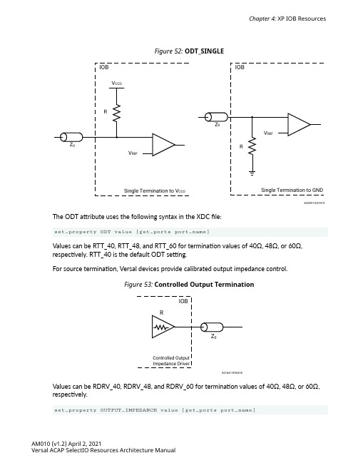
Figure 52: ODT_SINGLEX22491-041519 The ODT attribute uses the following syntax in the XDC file:set_property ODT value [get_ports port_name]Values can be RTT_40, RTT_48, and RTT_60 for termination values of 40Ω, 48Ω, or 60Ω, respectively. RTT_40 is the default ODT setting.For source termination, Versal devices provide calibrated output impedance control.Figure 53: Controlled Output TerminationX21641-092418Values can be RDRV_40, RDRV_48, and RDRV_60 for termination values of 40Ω, 48Ω, or 60Ω, respectively.set_property OUTPUT_IMPEDANCE value [get_ports port_name]Chapter 4: XP IOB ResourcesDCITERMDISABLEBidirectional primitives that use ODT (SPLIT or SINGLE) internal termination have a DCITERMDISABLE port that allows you to disable internal input termination.Asserting this port High can help save power during long periods of IDLE time on an interface. Differential Termination AttributeIn addition to calibrated impedance, a fixed precision 100Ω differential input impedance block is available in XP IOB input pairs to support LVDS15 and MIPI_DPHY. For both LVDS15 andMIPI_DPHY, the bank must be powered at the VCCO level (1.5V for LVDS15 or 1.2V forMPI_DPHY) to use the differential impedance block.The DIFF_TERM_ADV attribute can be set to TERM_100 or TERM_NONE (default) to enable internal 100Ω termination. It uses the following syntax in the XDC file:set_property DIFF_TERM_ADV [get_ports port_name]XP IOB Level Hold and Bias FeaturesThe XP IOB provides several weak hold and biasing features in Versal devices. These features are designed to provide a known level to a pin that is not actively driven.PULLUP, PULLDOWN, KEEPERAll XP IOB pins can enable a weak internal PULLUP bias to V CCO, a weak internal PULLDOWN to GND, or a weak internal KEEPER circuit that both pulls up to V CCO or pulls down to GND, based on the last driven pin voltage. The PULLTYPE attribute can be set to NONE, PULLUP, PULLDOWN, or KEEPER using the following syntax in the XDC file:set_property PULLTYPE value [get_ports port_name]DQS_BIAS, DC_BIAS, and AC CouplingDQS_BIASDQS_BIAS behaves as a logic 0 holding mechanism for undriven pins in pseudo-differential buffers (for example: DIFF_HSTL or DIFF_SSTL) by weakly pulling the P-side of the buffer to GND and the N-side of the buffer to V CCO. This allows an IDLE link to maintain a fixed logic level when a driver and termination are disabled on the link. The left circuit in the following figure shows DQS_BIAS behavior on pseudo-differential links.The allowed values for the DQS_BIAS attribute for applicable I/O standards are TRUE and FALSE (DEFAULT) and are enabled using the following syntax:set_property DQS_BIAS TRUE|FALSE [get_ports port_name]DC_BIASDC_BIAS provides an internal bias to both P and N pins used as an input in scenarios where an AC coupled differential signal needs to be re-biased such that the LVDS15 receiver specifications are met. The DC_BIAS feature creates a bias through an equivalent voltage divider network to the bank's V CCO. The DC_BIAS attribute can be added to the XDC:set_property DC_BIAS DC_BIAS_0|DC_BIAS_1|DC_BIAS_2|DC_BIAS_3 [get_portsport_name]The DC_BIAS_1 setting provides the equivalent to 192 Ω at 20% V CCO. In a 1.5V bank, the combination of DIFF_TERM_ADV and DC_BIAS_1 provide an appropriate termination and bias for an AC coupled LVDS link without the need for bias or termination components on the PCB. DC_BIAS_2 provides the equivalent of 48Ω to 20% V CCO, but is not recommended for use with AC coupling due to a higher current draw caused by the voltage divider used to generate the equivalent 48Ω voltage divider. DC_BIAS_3 provides a 50Ω to GND bias which has very limited practical use as a bias network. With a LVDS15 IOSTANDARD used in a 1.5V bank, the combination of DC_BIAS_1 and DIFF_TERM_ADV provide both a bias and termination appropriate for many differential signals that require AC coupling. Because DC_BIAS can corrupt a weaker driver, it should not be used when the IOB is configured as an output or bidirectional. Table 91: DC_BIAS Levels ExplainedDC_BIAS Attribute DescriptionDC_BIAS_0No BiasDC_BIAS_1192Ω to 20% V CCO. Suitable for AC coupling applicationsneeding a weaker bias. DIFF_TERM_ADV or equivalentexternal 100Ω termination should be used with DC_BIAS_1.DIFF_TERM_ADV is only available in a 1.5V V CCODC_BIAS_248Ω to 20% V CCO. Provides a strong bias and termination.DC_BIAS_2 should not be used with DIFF_TERM_ADV.DC_BIAS_350Ω to GND. Care must be taken to ensure that GND biasedsignal does not violate input lower levels outlined in thedata sheet.。
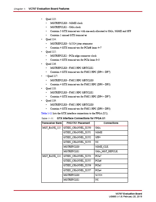
Chapter 1:VC707 Evaluation Board Features•Quad 113:•MGTREFCLK0 - SGMII clock•MGTREFCLK1 - SMA clock•Contains 3 GTX transceivers with one each allocated to SMA, SGMII and SFP•Contains 1 unused GTX transceiver•Quad 114:•MGTREFCLK0 - Si5324 jitter attenuator•Contains 4 GTX transceivers for PCIe® lanes 4–7•Quad 115:•MGTREFCLK1 - PCIe edge connector clock•Contains 4 GTX transceivers for PCIe lanes 0–3•Quad 116:•MGTREFCLK0 - FMC2 HPC GBTCLK1•Contains 4 GTX transceivers for FMC2 HPC (DP4 – DP7)•• Quad 117:•MGTREFCLK0 - FMC2 HPC GBTCLK0•Contains 4 GTX transceivers for FMC2 HPC (DP0 – DP3)•Quad 118:•MGTREFCLK0 - FMC1 HPC GBTCLK1•Contains 4 GTX transceivers for FMC1 HPC (DP4 – DP7)•Quad 119:•MGTREFCLK0 - FMC1 HPC GBTCLK0•Contains 4 GTX transceivers for FMC1 HPC (DP0 – DP3)Table1-11 lists the GTX interface connections to the FPGA (U1).Table 1-11: GTX Interface Connections for FPGA U1Transceiver Bank FHG1761 Placement ConnectionsMGT_BANK_113GTXE2_CHANNEL_X1Y0SMAGTXE2_CHANNEL_X1Y1SGMIIGTXE2_CHANNEL_X1Y2SFP+GTXE2_CHANNEL_X1Y3NCMGTREFCLK0SGMII_CLKMGTREFCLK1SMA_MGT_REFCLKMGT_BANK_114GTXE2_CHANNEL_X1Y4PCIe7GTXE2_CHANNEL_X1Y5PCIe6GTXE2_CHANNEL_X1Y6PCIe5GTXE2_CHANNEL_X1Y7PCIe4MGTREFCLK0Si5324MGTREFCLK1NCFeature DescriptionsVITA 57.1 FMC1 HPC Connector (Partially Populated)[Figure1-2, callout 30]The VC707 board implements two instances of the FMC HPC VITA 57.1 specification connector.This section discusses the FMC1 HPC J35 connector.Note:The FMC1 HPC J35 connector is a keyed connector oriented so that a plug-on card facesaway from the VC707 board.The VITA 57.1 FMC standard calls for two connector densities: a high pin count (HPC) and a lowpin count (LPC) implementation. A 400 pin 10x40 position connector form factor is used for bothversions. The HPC version is fully populated with all 400 pins present. The LPC version is partiallypopulated with 160 pins.The 10x40 rows of an FMC HPC connector provides pins for up to:•160 single-ended or 80 differential user-defined signals•10 GTX transceivers• 2 GTX clocks• 4 differential clocks•159 ground and 15 power connectionsThe VC707 board FMC1 HPC connector J35 implements a subset of the maximum signal and clockconnectivity capabilities:•80 differential user-defined pairs•34 LA pairs (LA00-LA33)•24 HA pairs (HA00-HA23)•22 HB pairs (HB00-HB21)•8 GTX transceivers• 2 GTX clocks• 2 differential clocksThe FMC1 HPC signals are distributed across GTX Quads 118 and 119. Each Quad has the VCCOvoltage connected to V ADJ.Note:The VC707 board VADJ voltage for the FMC1 HPC (J35) connector is determined by theFMC VADJ power sequencing logic described in FMC_VADJ Voltage Control.VITA 57.1 FMC2 HPC Connector (Partially Populated)[Figure1-2, callout 31]The VC707 board implements two instances of the FMC HPC VITA 57.1 specification connector.This section discusses the FMC2 HPC J37 connector.Note:The FMC2 HPC J37 connector is a keyed connector oriented so that a plug-on card facesaway from the VC707 board.The FMC standard calls for two connector densities: a High Pin Count (HPC) and a Low Pin Count(LPC) implementation. A 400pin 10x40 position connector form factor is used for both versions.The HPC version is fully populated with all 400 pins present. The LPC version is partially populatedwith 160 pins.Chapter 1:VC707 Evaluation Board FeaturesThe 10x40 rows of an FMC HPC connector provides pins for up to:•160 single-ended or 80 differential user-defined signals•10 GTX transceivers• 2 GTX clocks• 4 differential clocks•159 ground and 15 power connectionsThe VC707 board FMC2 HPC connector J37 implements a subset of the maximum signal and clockconnectivity capabilities:•58 differential user-defined pairs (as shipped with the Virtex-7 XC7VX485T-2FFG1761CFPGA installed on the VC707 board, the FMC2 HB00-HB21 bus connections are notsupported. Refer to the Virtex-7FPGA VC707 Evaluation Kit Master Answer Record inAppendix G: References for more information).•34 LA pairs (LA00-LA33)•24 HA pairs (HA00-HA23)•8 GTX transceivers• 2 GTX clocks• 2 differential clocksThe FMC2 HPC signals are distributed across GTX Quads 116 and 117. Each Quad has the VCCOvoltage connected to V ADJ.Note:The VC707 board VADJ voltage for the FMC2 HPC (J37) connector is determined by theFMC VADJ power sequencing logic described in FMC_VADJ Voltage Control.Signaling Speed Ratings:•Single-ended: 9GHz (18 Gb/s)•Differential•Optimal Vertical: 9GHz (18 Gb/s)•Optimal Horizontal: 16GHz (32 Gb/s)•High Density Vertical: 7GHz (15 Gb/s)Mechanical specifications:•Samtec SEAM/SEAF Series• 1.27 mm x 1.27 mm (0.050" x 0.050") pitchThe Samtec connector system is rated for signaling speeds up to 9GHz (18 Gb/s) based on a -3 dBinsertion loss point within a two-level signaling environment.Appendix A:Default Switch and Jumper SettingsAppendix B:VITA 57.1 FMC Connector Pinouts。
Chapter 4: XP IOB ResourcesDrive Strength Control and the VOH AttributeDRIVE Strength ControlLVCMOS drivers (LVCMOS12 and LVCMOS15) drivers support output drive strength control to size the driver output strength to the load driven. For a list of drive options and standards, seethe XP IOB Supported Standards section. Assigning the DRIVE property 2, 4, 6, 8, or 12(LVCMOS15 only) ensures that the XP IOB driver can meet valid logic thresholds for loads of 2 mA, 4 mA, 6 mA, 8 mA, or 12 mA, respectively. The DRIVE attribute uses the following syntax in the XDC file:set_property DRIVE value [get_ports port_name]VOH AttributeMIPI_DPHY, LVSTL_11, and DIFF_LVSTL_11 support the VOH attribute to help define the mode of the driver. VOH helps define the desired output high level for the driver. This can be used to define the use mode for a given standard. For LVSTL_11 and DIFF_LVSTL_11, the VOH attribute must be 50 (50% of V CCO). For MIPI_DPHY, the VOH attribute must be 28 (28% of V CCO). Forscenarios where an SSTL15 driver needs to drive a 1.8V SSTL receiver, a VOH attribute of 80adjusts the SSTL15 driver to be compatible with a 1.8V SSTL receiver. This option is limited in its scope to a single VOH option for a given standard. If not set, this property defaults to theappropriate VOH level.set_property VOH value [get_ports port_name]Slew ControlMost drivers support FAST, MEDIUM, and SLOW slew-rate options. These options can be used to optimize the edge rate of the driver for specific applications. For a list of IOSTANDARDS that support slew control see the XP IOB Supported Standards section.The SLEW attribute uses the following syntax in the XDC file:set_property SLEW value [get_ports port_name]AM010 (v1.2) April 2, 2021Versal ACAP SelectIO Resources Architecture ManualCalibrated Termination (Digitally Controlled Impedance)T o provide the highest precision termination, up to two external reference resistors per device must be provided to calibrate the internal device termination. Banks 700 and 800 (bank 800 does not exist in all devices) contain the IO_VR_700 and IO_VR_800 (not available on all devices) pins that must have a 240Ω reference resistor pulled up to the V CCO powering the referenced bank number (that is banks 700 or 800). The reference resistor is used to calibrate all I/O banks on the same half of the device. Banks 700 and 800 (when present) must always be powered by a validV CCOlevel.IMPORTANT! The IO_VR_700 and IO_VR_800 pins (not available on all devices) must have an external 240Ω resistor tied to VCCO_700 and VCCO_800 respectively. These pins are dedicated and can not be used as user I/O. All designs MUST populate these pins appropriately, regardless of the I/O standards used in a design.Figure 50: IO_VR_700 PinV CCO_700X22488-031519In previous FPGA generations,specific IOSTANDARDs ending in _DCI were required to enablethe internal calibration circuitry (DCI). In the Versal architecture, the reference calibrationcircuitry is always enabled and _DCI specific standards are not required to enable calibratedtermination.The XP IOB provides several types of calibrated termination:•Split-termination input impedance (termination to V CCO/2)•Single-termination input impedance (termination to V CCO or termination to GND)•Source terminationEach type of termination allows the selection of termination strengths to accommodate 40Ω,48Ω, and 60Ω interfaces. Single-termination input impedance offsets a pull type to either V CCO or GND depending on the standard (see the XP IOB Supported Standards section for furtherinformation).Chapter 4: XP IOB ResourcesAM010 (v1.2) April 2, 2021Versal ACAP SelectIO Resources Architecture ManualChapter 4: XP IOB ResourcesOn-Die Termination AttributeThe on-die termination (ODT) attribute supports split or single termination on the inputs of theHSTL, SSTL, POD, LVSTL, and HSUL standards. The advantage of using ODT over discreteresistors is that signal integrity is improved by completely removing any PCB trace stubs at thereceiver. The ODT attribute is used to define the value of the on-die termination at the input.The V CCO of the I/O bank must be connected to the appropriate voltage level for the ODTattribute to perform as expected. When ODT is used for differential buffers, both P and N pinshave the same termination.The ODT_SPLIT termination is for memory interfaces that use the SSTL or HSTL type I/Ostandards. SPLIT termination provides termination that centers the signal around the V REF inputthreshold level. As shown in the following diagram, in Versal devices this termination isimplemented internally with 2R pulled up to V CCO and 2R pulled down to GND, creating asymmetric equivalent termination of R to V CCO/2.Figure 51: ODT_SPLITstandards (POD or LVSTL). The standard used defines whether the ODT is terminated to V CCO or GND (see the supported I/O standards table) and is implemented with a single R structure toV CCO or GND as shown in the following figure.AM010 (v1.2) April 2, 2021Versal ACAP SelectIO Resources Architecture Manual。
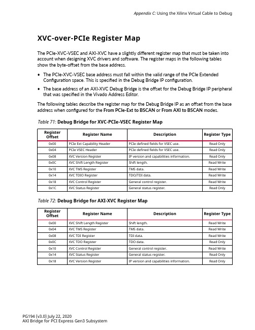
Appendix C: Using the Xilinx Virtual Cable to DebugXVC-over-PCIe Register MapThe PCIe-XVC-VSEC and AXI-XVC have a slightly different register map that must be taken into account when designing XVC drivers and software. The register maps in the following tablesshow the byte-offset from the base address.•The PCIe-XVC-VSEC base address must fall within the valid range of the PCIe Extended Configuration space. This is specified in the Debug Bridge IP configuration.•The base address of an AXI-XVC Debug Bridge is the offset for the Debug Bridge IP peripheral that was specified in the Vivado Address Editor.The following tables describe the register map for the Debug Bridge IP as an offset from the base address when configured for the From PCIe-Ext to BSCAN or From AXI to BSCAN modes.Table 71: Debug Bridge for XVC-PCIe-VSEC Register MapRegisterOffset Register Name Description Register Type0x00PCIe Ext Capability Header PCIe defined fields for VSEC use.Read Only0x04PCIe VSEC Header PCIe defined fields for VSEC use.Read Only0x08XVC Version Register IP version and capabilities information.Read Only0x0C XVC Shift Length Register Shift length.Read Write0x10XVC TMS Register TMS data.Read Write0x14XVC TDIO Register TDO/TDI data.Read Write0x18XVC Control Register General control register.Read Write0x1C XVC Status Register General status register.Read Only Table 72: Debug Bridge for AXI-XVC Register MapRegisterOffset Register Name Description Register Type0x00XVC Shift Length Register Shift length.Read Write0x04XVC TMS Register TMS data.Read Write0x08XVC TDI Register TDI data.Read Write0x0C XVC TDO Register TDO data.Read Only0x10XVC Control Register General control register.Read Write0x14XVC Status Register General status register.Read Only0x18XVC Version Register IP version and capabilities information.Read OnlyPG194 (v3.0) July 22, 2020AXI Bridge for PCI Express Gen3 SubsystemPCIe Ext Capability HeaderThis register is used to identify the PCIe-XVC-VSEC added to a PCIe design. The fields and values in the PCIe Ext Capability Header are defined by PCI-SIG and are used to identify the format of the extended capability and provide a pointer to the next extended capability, if applicable. When used as a PCIe-XVC-VSEC, the appropriate PCIe ID fields should be evaluated prior to interpretation. These can include PCIe Vendor ID, PCIe Device ID, PCIe Revision ID, Subsystem Vendor ID, and Subsystem ID. The provided drivers specifically check for a PCIe Vendor ID that matches Xilinx (0x10EE) before interpreting this register. The following table describes the fields within this register.Table 73: PCIe Ext Capability Header Register DescriptionBitLocation Field Description InitialValue Type15:0PCIeExtendedCapabilityIDThis field is a PCI-SIG defined ID number that indicates the natureand format of the Extended Capability. The Extended Capability IDfor a VSEC is 0x000B0x000B Read Only19:16CapabilityVersion This field is a PCI-SIG defined version number that indicates theversion of the capability structure present. Must be 0x1 for thisversion of the specification.0x1Read Only31:20NextCapabilityOffsetThis field is passed in from the user and contains the offset to thenext PCI Express Capability structure or 0x000 if no other itemsexist in the linked list of capabilities. For Extended Capabilitiesimplemented in the PCIe extended configuration space, this valuemust always be within the valid range of the PCIe ExtendedConfiguration space.0x000Read OnlyPCIe VSEC Header (PCIe-XVC-VSEC only)This register is used to identify the PCIe-XVC-VSEC when the Debug Bridge IP is in this mode. The fields are defined by PCI-SIG, but the values are specific to the Vendor ID (0x10EE for Xilinx). The PCIe Ext Capability Header register values should be qualified prior to interpreting this register.Table 74: PCIe XVC VSEC Header Register DescriptionBitLocation Field Description InitialValue Type15:0VSEC ID This field is the ID value that can be used to identify the PCIe-XVC-VSEC and is specific to the Vendor ID (0x10EE for Xilinx).0x0008Read Only19:16VSEC Rev This field is the Revision ID value that can be used to identify thePCIe-XVC-VSEC revision.0x0Read Only31:20VSECLength This field indicates the number of bytes in the entire PCIe-XVC-VSEC structure, including the PCIe Ext Capability Header and PCIeVSEC Header registers.0x020Read OnlyAppendix C: Using the Xilinx Virtual Cable to DebugPG194 (v3.0) July 22, 2020AXI Bridge for PCI Express Gen3 SubsystemAppendix C: Using the Xilinx Virtual Cable to DebugXVC Version Register (PCIe-XVC-VSEC only)This register is populated by the Xilinx tools and is used by the Vivado Design Suite to identifythe specific features of the Debug Bridge IP that is implemented in the hardware design.XVC Shift Length RegisterThis register is used to set the scan chain shift length within the debug scan chain.XVC TMS RegisterThis register is used to set the TMS data within the debug scan chain.XVC TDO/TDI Data Register(s)This register is used for TDO/TDI data access. When using PCIePCI-XVC-VSEC, these tworegisters are combined into a single field. When using AXI-XVC, these are implemented as twoseparate registers.XVC Control RegisterThis register is used for XVC control data.XVC Status RegisterThis register is used for XVC status information.XVC Driver and SoftwareExample XVC driver and software has been provided with the Vivado Design Suite installation, which is available at the following location:<Vivado_Installation_Path>/data/xicom/ driver/pcie/xvc_pcie.zip. This should be used for reference when integrating the XVCcapability into Xilinx FPGA platform design drivers and software. The provided Linux kernel mode driver and software implement XVC-over-PCIe debug for both PCIe-XVC-VSEC and AXI-XVCdebug bridge implementations.When operating in PCIe-XVC-VSEC mode, the driver will initiate PCIe configuration transactions to interface with the FPGA debug network. When operating in AXI-XVC mode, the driver willinitiate 32-bit PCIe Memory BAR transactions to interface with the FPGA debug network. Bydefault, the driver will attempt to discover the PCIe-XVC-VSEC and use AXI-XVC if the PCIe-XVC-VSEC is not found in the PCIe configuration extended capability linked list.PG194 (v3.0) July 22, 2020AXI Bridge for PCI Express Gen3 Subsystem。
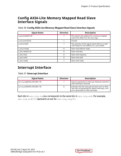
Chapter 3: Product SpecificationConfig AXI4-Lite Memory Mapped Read SlaveInterface SignalsTable 30: Config AXI4-Lite Memory Mapped Read Slave Interface SignalsSignal Name Direction Description s_axil_araddr[31:0]I This signal is the address for a memory mappedread to the DMA from the user logic.s_axil_arprot[2:0]I Unuseds_axil_arvalid I The assertion of this signal means there is a validread request to the address on s_axil_araddr.s_axil_arready O Slave read address ready.s_axil_rdata[31:0]O Slave read data.s_axil_rresp O Slave read response.s_axil_rvalid O Slave read valid.s_axil_rready I Slave read ready.Interrupt InterfaceTable 31: Interrupt InterfaceSignal Name Direction Description usr_irq_req[NUM_USR_IRQ-1:0]I Assert to generate an interrupt. Maintain assertionuntil interrupt is serviced.usr_irq_ack[NUM_USR_IRQ-1:0]O Indicates that the interrupt has been sent on PCIe.Two acks are generated for legacy interrupts. Oneack is generated for MSI interrupts.Each bits in usr_irq_req bus corresponds to the same bits in usr_irq_ack. For example,usr_irq_ack[0] represents an ack for usr_irq_req[0].PG195 (v4.1) April 29, 2021DMA/Bridge Subsystem for PCIe v4.1Send FeedbackSpartan-3 FPGA Family: Introduction and Ordering InformationDS099 (v3.1) June 27, 2013Product SpecificationChapter 3: Product SpecificationChannel 0-3 Status PortsTable 32: Channel 0-3 Status PortsSignal Name Direction Description h2c_sts [7:0]O Status bits for each channel. Bit:6: Control register 'Run' bit5: IRQ event pending4: Packet Done event (AXI4-Stream)3: Descriptor Done event. Pulses for one cycle foreach descriptor that is completed, regardless of thepleted field2: Status register Descriptor_stop bit1: Status register Descriptor_completed bit0: Status register busy bitc2h_sts [7:0]O Status bits for each channel. Bit:6: Control register 'Run' bit5: IRQ event pending4: Packet Done event (AXI4-Stream)3: Descriptor Done event. Pulses for one cycle foreach descriptor that is completed, regardless of thepleted field2: Status register Descriptor_stop bit1: Status register Descriptor_completed bit0: Status register busy bitConfiguration Extend Interface Port DescriptionsThe Configuration Extend interface allows the core to transfer configuration information with the user application when externally implemented configuration registers are implemented. Thefollowing table defines the ports in the Configuration Extend interface of the core.Note: This interface is not available for 7 series Gen2 IP.PG195 (v4.1) April 29, 2021DMA/Bridge Subsystem for PCIe v4.1Send FeedbackSpartan-3 FPGA Family: Introduction and Ordering InformationDS099 (v3.1) June 27, 2013Product SpecificationChapter 3: Product SpecificationTable 33: Configuration Extend Interface Port DescriptionsPort Direction Width Descriptioncfg_ext_read_received O1Configuration Extend Read ReceivedThe core asserts this output when it has received a configurationread request from the link. When neither user-implementedlegacy or extended configuration space is enabled, receipt of aconfiguration read results in a one-cycle assertion of this signal,together with valid cfg_ext_register_number andcfg_ext_function_number.When user-implemented legacy, extended configuration space,or both are enabled, for the cfg_ext_register_number fallingbelow mentioned ranges, this signal is asserted and the userlogic must present the cfg_ext_read_data andcfg_ext_read_data_valid.Legacy Space:0xB0-0xBFExtended Configuration space:0xE80 - 0xFFF (UltraScale+ HBM PCIe4C cores only)0x480 - 0x4FFcfg_ext_write_received O1Configuration Extend Write ReceivedThe core generates a one-cycle pulse on this output when it hasreceived a configuration write request from the link.cfg_ext_register_number O10Configuration Extend Register NumberThe 10-bit address of the configuration register being read orwritten. The data is valid when cfg_ext_read_received orcfg_ext_write_received is High.cfg_ext_function_number O8Configuration Extend Function NumberThe 8-bit function number corresponding to the configurationread or write request. The data is valid whencfg_ext_read_received or cfg_ext_write_received is High.cfg_ext_write_data O32Configuration Extend Write DataData being written into a configuration register. This output isvalid when cfg_ext_write_received is High.cfg_ext_write_byte_enable O4Configuration Extend Write Byte Enable Byte enables for aconfiguration write transaction.cfg_ext_read_data I32Configuration Extend Read DataYou can provide data from an externally implementedconfiguration register to the core through this bus. The coresamples this data on the next positive edge of the clock after itsets cfg_ext_read_received High, if you have setcfg_ext_read_data_valid.cfg_ext_read_data_valid I1Configuration Extend Read Data ValidThe user application asserts this input to the core to supply datafrom an externally implemented configuration register. The coresamples this input data on the next positive edge of the clockafter it sets cfg_ext_read_received High.Configuration Management Interface PortsThe Configuration Management interface is used to read and write to the Configuration SpaceRegisters. The following table defines the ports in the Configuration Management interface ofthe core.PG195 (v4.1) April 29, 2021DMA/Bridge Subsystem for PCIe v4.1Send Feedback。
9.Double-click the Debug Bridge IP identified as xvc_vsec to view the configuration optionfor this IP. Make note of the following configuration parameters because they will be used to configure the driver.•PCIe XVC VSEC ID (default 0x0008)•PCIe XVC VSEC Rev ID (default 0x0)IMPORTANT! Do not modify these parameter values when using a Xilinx Vendor ID or provided XVC driversand software. These values are used to detect the XVC extended capability. (See the PCIe specification for additional details.)In the Flow Navigator, click Generate Bitstream to generate a bitstream for the example design project. This bitstream will be then be loaded onto the FPGA board to enable XVC debug over PCIe.After the XVC-over-PCIe hardware design has been completed, an appropriate XVC enabled PCIe driver and associated XVC-Server software application can be used to connect the Vivado Design Suite to the PCIe connected FPGA. Vivado can connect to an XVC-Server application that is running local on the same Machine or remotely on another machine using a TCP/IP socket.System Bring-UpThe first step is to program the FPGA and power on the system such that the PCIe link is detected by the host system. This can be accomplished by either:•Programming the design file into the flash present on the FPGA board, or•Programming the device directly via JTAG.If the card is powered by the Host PC, it will need to be powered on to perform this programming using JTAG and then re-started to allow the PCIe link to enumerate. After the system is up and running, you can use the Linux lspci utility to list out the details for the FPGA-based PCIe device.Compiling and Loading the DriverThe provided PCIe drivers and software should be customized to a specific platform. T o accomplish this, drivers and software are normally developed to verify the Vendor ID, Device ID, Revision ID, Subsystem Vendor ID, and Subsystem ID before attempting to access device-extended capabilities or peripherals like the PCIe-XVC-VSEC or AXI-XVC. Because the provided driver is generic, it only verifies the Vendor ID and Device ID for compatibility before attempting to identify the PCIe-XVC-VSEC or AXI-XVC peripheral.The XVC driver and software are provide as a ZIP file included with the Vivado Design Suite installation.1.Copy the ZIP file from the Vivado install directory to the FPGA connected Host PC andextract (unzip) its contents. This file is located at the following path within the Vivadoinstallation directory.XVC Driver and SW Path: …/data/xicom/driver/pcie/xvc_pcie.zipThe README.txt files within the driver_* and xvcserver directories identify how to compile, install, and run the XVC drivers and software, and are summarized in the following steps. Follow the following steps after the driver and software files have been copied to the Host PC and you are logged in as a user with root permissions.2.Modify the variables within the driver_*/xvc_pcie_user_config.h file to match yourhardware design and IP settings. Consider modifying the following variables:•PCIE_VENDOR_ID: The PCIe Vendor ID defined in the PCIe® IP customization.•PCIE_DEVICE_ID: The PCIe Device ID defined in the PCIe® IP customization.•Config_space: Allows for the selection between using a PCIe-XVC-VSEC or an AXI-XVCperipheral. The default value of AUTO first attempts to discover the PCIe-XVC-VSEC, then attempts to connect to an AXI-XVC peripheral if the PCIe-XVC-VSEC is not found. A valueof CONFIG or BAR can be used to explicitly select between PCIe®-XVC-VSEC and AXI-XVC implementations, as desired.•config_vsec_id: The PCIe XVC VSEC ID (default 0x0008) defined in the Debug Bridge IP when the Bridge Type is configured for From PCIE to BSCAN. This value is only used for detection of the PCIe®-XVC-VSEC.•config_vsec_rev: The PCIe XVC VSEC Rev ID (default 0x0) defined in the Debug Bridge IP when the Bridge Type is configured for From PCIe to BSCAN. This value is only used for detection of the PCIe-XVC-VSEC.•bar_index: The PCIe BAR index that should be used to access the Debug Bridge IP whenthe Bridge Type is configured for From AXI to BSCAN. This BAR index is specified as acombination of the PCIe IP customization and the addressable AXI peripherals in yoursystem design. This value is only used for detection of an AXI-XVC peripheral.•bar_offset: PCIe BAR Offset that should be used to access the Debug Bridge IP when theBridge Type is configured for From AXI to BSCAN. This BAR offset is specified as acombination of the PCIe IP customization and the addressable AXI peripherals in yoursystem design. This value is only used for detection of an AXI-XVC peripheral.3.Move the source files to the directory of your choice. For example, use:/home/username/xil_xvc or /usr/local/src/xil_xvc4.Make sure you have root permissions and change to the directory containing the driver files.# cd /driver_*/pile the driver module:# make installThe kernel module object file will be installed as:/lib/modules/[KERNEL_VERSION]/kernel/drivers/pci/pcie/Xilinx/xil_xvc_driver.ko6.Run the depmod command to pick up newly installed kernel modules:# depmod -a7.Make sure no older versions of the driver are loaded:# modprobe -r xil_xvc_driver8.Load the module:# modprobe xil_xvc_driverIf you run the dmesg command, you will see the following message:kernel: xil_xvc_driver: Starting…Note: You can also use insmod on the kernel object file to load the module:# insmod xil_xvc_driver.koHowever, this is not recommended unless necessary for compatibility with older kernels.9.The resulting character file,/dev/xil_xvc/cfg_ioc0, is owned by user root and grouproot, and it will need to have permissions of 660. Change permissions on this file if it does not allow the application to interact with the driver.# chmod 660 /dev/xil_xvc/cfg_ioc010.Build the simple test program for the driver:# make test11.Run the test program:# ./driver_test/verify_xil_xvc_driverYou should see various successful tests of differing lengths, followed by the followingmessage:"XVC PCIE Driver Verified Successfully!"Compiling and Launching the XVC-Server Application The XVC-Server application provides the connection between the Vivado HW server and the XVC enabled PCIe device driver. The Vivado Design Suite connects to the XVC-Server using TCP/IP. The desired port number will need to be exposed appropriately through the firewalls for your network. The following steps can be used to compile and launch the XVC software application, using the default port number of 10200.Make sure the firewall settings on the system expose the port that will be used to connect to the Vivado Design Suite. For this example, port 10200 is used.。
CCLK: Configuration ClockThe configuration clock signal on this pin synchronizes the reading or writing of configuration data. The CCLK pin is an input-only pin for the Slave Serial and Slave Parallel configuration modes. In the Master Serial and Master Parallel configuration modes, the FPGA drives the CCLK pin and CCLK should be treated as a full bidirectional I/O pin for signal integrity analysis.Although the CCLK frequency is relatively low, Spartan-3 FPGA output edge rates are fast. Any potential signal integrity problems on the CCLK board trace can cause FPGA configuration to fail. Therefore, pay careful attention to the CCLK signal integrity on the printed circuit board. Signal integrity simulation with IBIS is recommended. For all configuration modes except JTAG, consider the signal integrity at every CCLK trace destination, including the FPGA’s CCLK pin. For more details on CCLK design considerations, see Chapter 2 of UG332, Spartan-3 Generation Configuration User Guide.During configuration, the CCLK pin has a pull-up resistor to VCCAUX, regardless of the HSWAP_EN pin. After configuration, the CCLK pin is pulled High to VCCAUX by default as defined by the CclkPin bitstream selection, although this behavior is programmable. Any clocks applied to CCLK after configuration are ignored unless the bitstream option Persist is set to Yes, which retains the configuration interface. Persist is set to No by default. However, if Persist is set to Yes, then all clock edges are potentially active events, depending on the other configuration control signals.The bitstream generator option ConfigRate determines the frequency of the internally-generated CCLK oscillator required for the Master configuration modes. The actual frequency is approximate due to the characteristics of the silicon oscillator and varies by up to 50% over the temperature and voltage range. By default, CCLK operates at approximately 6 MHz. Via the ConfigRate option, the oscillator frequency is set at approximately 3, 6, 12, 25, or 50 MHz. At power-on, CCLK always starts operation at its lowest frequency. The device does not start operating at the higher frequency until the ConfigRate control bits are loaded during the configuration process.PROG_B: Program/Configure DeviceThis asynchronous pin initiates the configuration or re-configuration processes. A Low-going pulse resets the configuration logic, initializing the configuration memory. This initialization process cannot finish until PROG_B returns High. Asserting PROG_B Low for an extended period delays the configuration process. At power-up, there is always a pull-up resistor to VCCAUX on this pin, regardless of the HSWAP_EN input. After configuration, the bitstream generator option ProgPin determines whether or not the pull-up resistor is present. By default, the ProgPin option retains the pull-up resistor.After configuration, hold the PROG_B input High. Any Low-going pulse on PROG_B lasting 300ns or longer restarts the configuration process.Table 73:PROG_B OperationDONE: Configuration Done, Delay Start-Up SequenceThe FPGA produces a Low-to-High transition on this pin indicating that the configuration process is complete. The bitstream generator option DriveDone determines whether this pin functions as a totem-pole output that can drive High or as an open-drain output. If configured as an open-drain output—which is the default behavior—then a pull-up resistor is required to produce a High logic level. There is a bitstream option that provides an internal pull-up resistor, otherwise an external pull-up resistor is required.The open-drain option permits the DONE lines of multiple FPGAs to be tied together, so that the common node transitions High only after all of the FPGAs have completed configuration. Externally holding the open-drain DONE pin Low delays the start-up sequence, which marks the transition to user mode.Package Thermal CharacteristicsThe power dissipated by an FPGA application has implications on package selection and system design. The power consumed by a Spartan-3 FPGA is reported using either the XPower Estimator (XPE) or the XPower Analyzer integrated in the Xilinx ISE development software. T able86 provides the thermal characteristics for the various Spartan-3 device/package offerings.The junction-to-case thermal resistance (θJC) indicates the difference between the temperature measured on the package body (case) and the die junction temperature per watt of power consumption. The junction-to-board (θJB) value similarly reports the difference between the board and junction temperature. The junction-to-ambient (θJA) value reports the temperature difference per watt between the ambient environment and the junction temperature. The θJA value is reported at different air velocities, measured in linear feet per minute (LFM). The “Still Air (0 LFM)” column shows the θJA value in a system without a fan. The thermal resistance drops with increasing air flow.Table 86:Spartan-3 FPGA Package Thermal CharacteristicsPackage Device Junction-to-Case (θJC)Junction-to-Board (θJB)Junction-to-Ambient (θJA) at Different Air FlowsUnitsStill Air(0 LFM)250 LFM500 LFM750 LFMVQ(G)100XC3S5012.0–46.238.435.834.9°C/Watt XC3S20010.0–40.533.731.330.5°C/WattCP(G)132(1)XC3S5014.532.853.046.444.042.5°C/WattTQ(G)144XC3S507.6–41.031.927.225.6°C/Watt XC3S200 6.6–34.526.923.021.6°C/Watt XC3S400 6.1–32.825.521.820.4°C/WattPQ(G)208XC3S5010.6–37.427.624.422.6°C/Watt XC3S2008.6–36.226.723.621.9°C/Watt XC3S4007.5–35.426.123.121.4°C/WattFT(G)256XC3S2009.922.931.725.624.524.2°C/Watt XC3S4007.919.028.422.821.521.0°C/Watt XC3S1000 5.614.724.819.218.017.5°C/WattFG(G)320XC3S4008.913.924.419.017.817.0°C/Watt XC3S10007.811.822.317.015.815.0°C/Watt XC3S1500 6.79.820.315.1813.813.1°C/WattFG(G)456XC3S4008.413.620.815.113.913.4°C/Watt XC3S1000 6.410.619.313.412.311.7°C/Watt XC3S1500 4.98.318.312.411.210.7°C/Watt XC3S2000 3.7 6.517.711.710.510.0°C/WattFG(G)676XC3S1000 6.010.417.913.712.612.0°C/Watt XC3S1500 4.98.816.812.411.310.7°C/Watt XC3S2000 4.17.915.611.19.99.3°C/Watt XC3S4000 3.67.015.010.59.38.7°C/Watt XC3S5000 3.4 6.314.710.39.18.5°C/WattFG(G)900XC3S2000 3.77.014.310.39.38.8°C/Watt XC3S4000 3.3 6.413.69.78.78.2°C/Watt XC3S5000 2.9 5.913.19.28.17.6°C/Watt5IO_L32P_5/GCLK2P52GCLK 6IO_L01N_6/VRP_6P36DCI 6IO_L01P_6/VRN_6P35DCI 6IO_L20N_6P33I/O 6IO_L20P_6P32I/O 6IO_L21N_6P31I/O 6IO_L21P_6P30I/O 6IO_L22N_6P28I/O 6IO_L22P_6P27I/O 6IO_L23N_6P26I/O 6IO_L23P_6P25I/O 6IO_L24N_6/VREF_6P24VREF 6IO_L24P_6P23I/O 6IO_L40N_6P21I/O 6IO_L40P_6/VREF_6P20VREF 7IO/VREF_7P4VREF 7IO_L01N_7/VRP_7P2DCI 7IO_L01P_7/VRN_7P1DCI 7IO_L20N_7P6I/O 7IO_L20P_7P5I/O 7IO_L21N_7P8I/O 7IO_L21P_7P7I/O 7IO_L22N_7P11I/O 7IO_L22P_7P10I/O 7IO_L23N_7P13I/O 7IO_L23P_7P12I/O 7IO_L24N_7P15I/O 7IO_L24P_7P14I/O 7IO_L40N_7/VREF_7P18VREF 7IO_L40P_7P17I/O 0,1VCCO_TOP P126VCCO 0,1VCCO_TOP P138VCCO 0,1VCCO_TOP P115VCCO 2,3VCCO_RIGHT P106VCCO 2,3VCCO_RIGHT P75VCCO 2,3VCCO_RIGHT P91VCCO 4,5VCCO_BOTTOM P54VCCO 4,5VCCO_BOTTOM P43VCCO 4,5VCCO_BOTTOM P66VCCO 6,7VCCO_LEFTP19VCCOTable 91:TQ144 Package Pinout (Cont’d)Bank XC3S50, XC3S200, XC3S400 Pin Name TQ144 Pin NumberType。
Chapter 5:Dynamic Reconfiguration Port (DRP)Changing the Multiply and Divide ValuesThe Multiply and Divide (M/D) values can be directly programmed in the DCM through the DRP by reading from and writing to hex address 50h . The user application must read from address 50h first if either the M or the D value is changed. The M value must be masked into the most significant byte and the D value must be masked into the leastsignificant byte of the 16-bit DRP data word. The entire word is then written back. If both values are changed at the same time, only a write cycle is required.The DCM must be held in reset by activating input RST while changing the M/D values. At some point after RST is released, signal LOCKED goes true, indicating that the clock outputs of the DCM are valid.Table 5-1:Port Signal Definitions Signal NameDirection (1)DescriptionDCLK InputThe rising edge of this signal is the timing reference for all the other port signals. The required hold time for the other input signals relative to the rising edge of DCLK is zero (maximum). Normally, DCLK is driven with a global clock buffer.DEN InputThis signal enables all port operations. If DWE is FALSE, it is a read operation, otherwise a writeoperation. For any given DCLK cycle, all other input signals are don't care if DEN is not active. DEN should only be pulsed for one DCLK cycle.DWE InputWhen active, this signal enables a write operation to the port (see DEN, above). DWE should only be pulsed for one DCLK cycle.DADDR[m:0]InputThe value on this bus specifies the individual cell that is written or read on the next cycle of DCLK. The address is presented in the cycle that DEN is active.DI[n:0]InputThe value on this bus is the data that is written to the addressed cell. The data is presented in the cycle that DEN and DWE are active, and is captured in a register at the end of that cycle, but the actual write occurs at an unspecified time before DRDY is returned.DO[n:0]OutputIf DWE was inactive when DEN was activated, the value on this bus when DRDY goes active is the data read from the addressed cell. At all other times, the value on DO[n:0] is undefined.DRDY OutputThis signal is a response to DEN to indicate that the DRP cycle is complete and another DRP cycle can beinitiated. In the case of a port read, the DO bus must be captured on the rising edge of DCLK in the cycle that DRDY is active. The earliest that DEN can go active to start the next port cycle is the same clock cycle that DRDY is active.Notes:1.Input denotes input (write) to the DRP.Configuration RegistersTable 6-10:Configuration Options Register 0 DescriptionName Bit Index DescriptionCRC_BYPASS28Allows bypass of CRC when a special CRC value is loaded (0xDEFC):0:CRC enabled1:CRC disabledPWRDWN_STAT27Changes the DONE pin to a Powerdown status pin: 0:DONE pin1:Powerdown pinDONE_PIPE250:No pipeline stage for DONEIN1:Add pipeline stage for DONEINThe FPGA waits on DONE that is delayed by one StartupClk cycle. Use this option when StartupClk is running at high speeds.DRIVE_DONE240:DONE pin is open drain1:DONE is actively driven HighSINGLE230:Readback is not single-shotNew captured values are loaded on each successive CAP assertion on the CAPTURE_VIRTEX5 primitive. Capture can also be performed with the GCAPTURE instruction in the CMD register.1:Readback is single-shot.The RCAP instruction must be loaded into the CMD register between successive readbacks.OSCFSEL[22:17]Select CCLK frequency in Master modes (2MHz–60MHz)SSCLKSRC[16:15]Startup-sequence clock source.00:CCLK01:UserClk (per connection on the CAPTURE_VIRTEX5 block)1x:JTAGClkDONE_CYCLE[14:12]Startup cycle to release the DONE pin. 000:Startup phase 1001:Startup phase 2010:Startup phase 3011:Startup phase 4100:Startup phase 5101:Startup phase 6110:Startup phase 7111:KeepChapter 6:Configuration DetailsWatchdogFPGA End of StartupTo use the Watchdog to monitor the bitstream configuration, set TIMER_CFG_MON to 1 and the desired TIMER_VALUE in a write to the TIMER register in the bitstream. The TIMER_VALUE should be adequate to cover the entire FPGA configuration time until startup is complete. Any wait time in startup for DCI match, DCM lock, or DONE should also be included.Once enabled, the watchdog timer starts to count down. If the timer reaches 0 and the FPGA has not reached the final state of startup, a watchdog time-out error occurs and triggers a fallback configuration.User OperationTo use the Watchdog to monitor the user logic, set TIMER_USR_MON to 1 and the desired TIMER_VALUE in a write to the TIMER register in the bitstream. The user must constantly reset the watchdog counter before it times out, either by the LTIMER command or by directly accessing the TIMER register. The watchdog is automatically disabled when the device is shut down or on power down (including shutdown).Table 8-6 shows an example bitstream for reloading the Watchdog using the LTIMER command.Table 8-7 shows an example bitstream for directly accessing the TIMER register:Table 8-6:Example Bitstream for Reloading the Watchdog with LTIMERConfiguration Data(hex)Explanation FFFFFFFF Dummy Word AA995566 Sync Word 20000000 Type 1 NO OP30008001 Type 1 Write 1 Words to CMD00000000 NULL 20000000 Type 1 NO OP30008001 Type 1 Write 1 Words to CMD00000011 LTIMER Command 20000000 Type 1 NO OP30008001 Type 1 Write 1 Words to CMD0000000D DESYNCH 20000000Type 1 NO OPTable 8-7:Example Bitstream for Accessing the TIMER RegisterConfiguration Data(hex)Explanation FFFFFFFF Dummy Word AA995566Sync WordChapter 9:Readback CRC。
Table 3: Global SignalsSignal Name I/O Descriptionrefclk I AXI Bridge for PCIe Gen3 only:Virtex®-7: PCIe Reference Clock. Should be driven from the O port of reference clock IBUFDS_GTE2. UltraScale™: Dynamic reconfiguration port (DRP) Clock and Internal System Clock (Half frequency from sys_clk_gt frequency if PCIe Reference Clock is 250 MHz, otherwise same frequency as sys_clk_gt frequency). Should be driven by the ODIV2 port of reference clock IBUFDS_GTE3.sys_clk I DMA/Bridge Subsystem for PCIe in AXI Bridge mode only:UltraScale+: Dynamic reconfiguration port (DRP) Clock and Internal System Clock (Half frequency from sys_clk_gt frequency if PCIe Reference Clock is 250 MHz, otherwise same frequency as sys_clk_gt frequency). Should be driven by the ODIV2 port of reference clock IBUFDS_GTE4.sys_clk_gt I PCIe Reference Clock.UltraScale: Should be driven from the O port of reference clock IBUFDS_GTE3.UltraScale+: Should be driven from the O port of reference clock IBUFDS_GTE4.sys_rst_n I Reset from the PCIe edge connector reset signal.axi_aclk O AXI Bridge for PCIe Gen3: PCIe derived clock output for M_AXI, S_AXI interfaces, and all interrupt sideband (MSI, MSI-X, and Bridge Mode Interrupt) signals.DMA/Bridge Subsystem for PCIe in AXI Bridge mode: PCIe derived clock output for M_AXIB,S_AXIB, and S_AXIL interfaces. axi_aclk is a derived clock from the TXOUTCLK pin from the GT block; it is not expected to run continuously whileaxi_aresetn is asserted.axi_ctl_aclk I AXI Bridge for PCIe Gen3 only:aclk for the S_AXI_CTL interface. Recommended to be driven by the axi_aclk output. axi_ctl_aclk is a derived clock from the TXOUTCLK pin from the GT block; it is not expected to run continuously while axi_ctl_aresetn is asserted.This pin is for legacy use mode only. By default, new IP generation will have this clock pin internally driven by the IP. Use axi_aclk pin to clock the design.interrupt_out O Interrupt signal. It is asserted for as long as there exists at least one bit asserted in the Interrupt Decode register and is not masked in the Interrupt Mask register, and/or asserted in the Interrupt Decode 2 register and is not masked in the Interrupt Decode 2 Mask register.interrupt_out_msi_vec0to31O Interrupt signal. It is asserted for as long as thereexists at least one bit asserted in the Root Port MSIInterrupt Decode 1 register and is not masked inthe Root Port MSI Interrupt Decode 1 Maskregister.Only available in Root Port configuration withInterrupt Decode modeChapter 3: Product SpecificationTable 3: Global Signals (cont'd)Signal Name I/O Descriptiondma_bridge_resetn I Optional pin available to DMA/Bridge Subsystem for PCIe in AXI Bridge mode only and appears only when SOFT_RESET_EN parameter is set to TRUE. This pin is intended to be user driven reset when link down, Function Level Reset, Dynamic Function eXchange, or another error condition defined by user has occurred. It is not required to be toggled during initial link up operation.When used, all PCIe traffic must be in quiesce state. The signal must be asserted for longer than the Completion Timeout value (typically 50 ms).0: Resets all internal Bridge engines and registers as well as asserts axi_aresetn and axi_ctl_aresetn signals while maintaining PCIe link up.1: Normal operation.AXI Slave InterfaceFor all signals in this interface, s_axi_* is used for the AXI Bridge for PCIe Gen3 core, and s_axib_* is used for the DMA/Bridge Subsystem for PCIe in AXI Bridge mode.Table 4: AXI Slave Interface SignalsSignal Name I/O Descriptions_axi(b)_awid[c_s_axi_id_width-1:0]I Slave write address IDs_axi(b)_awaddr[axi_addr_width-1:0]I Slave write addresss_axi(b)_awregion[3:0]I Slave write region decodes_axi(b)_awlen[7:0]I Slave write burst lengths_axi(b)_awsize[2:0]I Slave write burst sizes_axi(b)_awburst[1:0]I Slave write burst types_axi(b)_awvalid I Slave address write valids_axi(b)_awready O Slave address write readys_axi(b)_wdata[axi_data_width-1:0]I Slave write datas_axi(b)_wstrb[axi_data_width/8-1:0]I Slave write strobes_axi(b)_wlast I Slave write lasts_axi(b)_wvalid I Slave write valids_axi(b)_wready O Slave write readys_axi(b)_wuser I Reserved. Tie to GND.Note: This signal is disabled for AXI Bridge for PCI Express Gen3. This signal is also disabled for the DMA/Bridge Subsystem for PCIe in AXI Bridge mode unless CONFIG.parity_settings = Propagate_Parity is set.s_axi(b)_bid[c_s_axi_id_width-1:0]O Slave response ID s_axi(b)_bresp[1:0]O Slave write response。
Configuration Data File FormatsConfiguration Data File FormatsXilinx design tools can generate configuration data files in a number of different formats, as described in Table 5-4. BitGen converts the post-PAR NCD file into a configuration file or a bitstream. PROMGen, the PROM file generator, converts one or more bitstream files into a PROM file. PROM files can be generated in a number of different file formats and does not need to be used with a PROM. They can be stored anywhere and delivered by any means.Bitstream OverviewThe Spartan-6 FPGA bitstream contains commands to the FPGA configuration logic as well as configuration data. Table 5-5 gives a typical default bitstream length for each of the Spartan-6 devices. Compression can provide a smaller bitstream.Table 5-4:Configuration File Formats File ExtensionBit Swapping (1)Xilinx SoftwareTool (2)Description BIT NotBit SwappedBitGen (generated by default)Binary configuration data file containing header information that does not need to be downloaded to the FPGA. Used to program devices from iMPACT software with a programming cable. RBT NotBit SwappedBitGen (generated if -b option is set)ASCII equivalent of the BIT file containing a text header and ASCII 1s and 0s. (Eight bits per configuration bit.)BIN NotBit Swapped BitGen (generated if -g Binary:yes option is set) orPROMGenBinary configuration data file with no header information. Similar to BIT file. Can be used for custom configuration solutions (for example, microprocessors), or in some cases to program third-party devices.MCS EXO Bit Swapped PROMGen oriMPACT softwareASCII PROM file formats containing address and checksum information in addition to configuration data. Used mainly for device programmers and iMPACT software.HEX Determined by User PROMGen oriMPACT softwareASCII PROM file format containing only configuration data. Used mainly in custom configuration solutions.CFIN/APROMGen oriMPACT software Data file used by iMPACT software to determine PROM options to set such as x2 and x4 data width or version control. Notes: 1.Bit swapping is discussed in the Bit Swapping section.2.For complete BitGen and PROMGen syntax, refer to UG628, Command Line Tools User Guide .Table 5-5:Spartan-6 FPGA Bitstream LengthDeviceTotal Number of Configuration Bits (1)6SLX42,731,4886SLX92,742,5286SLX163,731,2646SLX256,440,4326SLX25T 6,440,432Generating PROM Files in x16 mode. The FPGA now knows on which bus width to receive the rest of the data. Nopacket processed by the FPGA until the Sync word is found. See Table5-7.Table 5-7:Sync Word31:2423:1615:87:00xAA0x990x550x66Generating PROM FilesPROM files are generated from bitstream files with the PROMGen utility. Users can accessPROMGen directly from the command line or indirectly through the iMPACT FileGeneration Mode. For PROMGen syntax, refer to UG628, Command Line Tools User Guide.For information on iMPACT software, refer to the ISE® software documentation. PROMfiles serve to reformat bitstream files for PROM programming and combine bitstream filesfor serial daisy-chains (see PROM Files for Serial Daisy-Chains).PROM Files for Serial Daisy-ChainsConfiguration data for serial daisy-chains requires special formatting because separateBIT files cannot simply be concatenated together to program the daisy-chain. The specialformatting is performed by PROMGen (or iMPACT software) when generating a PROMfile from multiple bitstreams. To generate the PROM file, specify multiple bitstreams usingthe PROMGen -n, -u, and -d options or the iMPACT Software File Generation Wizard.Refer to ISE software documentation for details.PROMGen reformats the configuration bitstreams by nesting downstream configurationdata into configuration packets for upstream devices. Attempting to program the chain bysending multiple bitstreams to the first device causes the first device to configure and thenignore the subsequent data.PROM Files for SelectMAP ConfigurationThe MCS file format is most commonly used to program Xilinx® configuration PROMsthat in turn program a single FPGA in SelectMAP mode. For custom configurationsolutions, the BIN and HEX files are the easiest PROM file formats to use due to their rawdata format. In some cases, additional formatting is required; refer to XAPP502, Using aMicroprocessor to Configure Xilinx FPGAs via Slave Serial or SelectMAP Mode for details.If multiple configuration bitstreams for a SelectMAP configuration reside on a singlememory device, the bitstreams must not be combined into a serial daisy-chain PROM file.Instead, the target memory device should be programmed with multiple BIN or HEX files.If a single PROM file with multiple, separate data streams is needed, one can be generatedin iMPACT software by targeting a Parallel PROM, then selecting the appropriate numberof data streams. This can also be accomplished through the PROMGen command line.Refer to PROMGen software documentation for details.PROM Files for SPI/BPI ConfigurationThe -d, -u, -spi, -s, and -data_width options in PROMGen or the iMPACT SoftwareFile Generation Wizard are used to create PROM files for third-party flash devices. Theoutput format supported by the third-party programmer is important. Some BPI devicesrequire endian-swapping to be enabled when programming the PROM file. Refer to theflash vendor's documentation.eFUSE After configuration, the device cannot be reconfigured without toggling the PROGRAM_Bpin, cycling power, or issuing the JPROGRAM instruction. Fallback reconfiguration andIPROG reconfiguration (see Fallback MultiBoot, page134) are disabled after encryption isturned on. Readback is available through the ICAP primitive (see Bitstream Encryptionand Internal Configuration Access Port (ICAP)). None of these events resets the key ifV BATT or V CCAUX is maintained.A mismatch between the key used to generate the encrypted bitstream and the key storedin the device causes configuration to fail with the INIT_B pin going Low and the DONEpin remaining Low.Bitstream Encryption and Internal Configuration Access Port (ICAP)The Internal Configuration Access Port (ICAP) primitive provides the user logic withaccess to the Spartan-6 FPGA configuration interface. The ICAP interface is similar to theSelectMAP interface, although the restrictions on readback for the SelectMAP interface donot apply to the ICAP interface after configuration. Users can perform readback throughthe ICAP interface even if bitstream encryption is used. Unless the designer wires the ICAPinterface to user I/O, this interface does not offer attackers a method for defeating theSpartan-6 FPGA AES encryption scheme.Users concerned about the security of their design should not:•Wire the ICAP interface to user I/O-or-•Instantiate the ICAP primitive.Like the other configuration interfaces, the ICAP interface does not provide access to thekey register.V BATTThe encryption key memory cells are volatile and must receive continuous power to retaintheir contents. During normal operation, these memory cells are powered by the auxiliaryvoltage input (V CCAUX), although a separate V BATT power input is provided for retainingthe key when V CCAUX is removed. Because V BATT draws very little current (on the order ofnanoamperes), a small watch battery is suitable for this supply. (To estimate the battery life,refer to V BATT DC Characteristics in the Spartan-6 FPGA Data Sheet: DC and SwitchingCharacteristics and the battery specifications.) At less than a 150nA load, the endurance ofthe battery should be limited only by its shelf life.V BATT does not draw any current and can be removed while V CCAUX is applied. V BATTcannot be used for any purpose other than retaining the encryption keys when V CCAUX isremoved.eFUSEThe fuse link is programmed by flowing a large current for a specific amount of time. Fuseprogramming current is provided by a fixed external voltage supply (V FS pin). Themaximum level is controlled by an internally generated supply. eFUSEs are one-timeprogrammable.The resistance of a programmed fuse link is typically a few orders of magnitude higherthan that of a pristine one. A programmed fuse is assigned a logic value of 1 and a pristinefuse 0.Chapter 6:Readback and Configuration VerificationChapter 8:Readback CRC。