1.5寸电子墨水屏规格书
- 格式:pdf
- 大小:2.13 MB
- 文档页数:32
35寸电阻屏规格书
以下是35寸电阻屏的一般规格书内容:
1. 屏幕尺寸:35英寸(对角线)
2. 分辨率:通常为1920x1080像素,即1080p全高清分辨率
3. 显示比例:16:9
4. 亮度:通常为200-300尼特(cd/m²)
5. 对比度:通常为1000:1
6. 视角:通常为178度(水平和垂直)
7. 颜色显示能力:通常为16.7百万色
8. 反应时间:通常为5毫秒或更低
9. 触摸技术:电阻式触控技术
10. 触摸点数:通常为10个点触控
11. 刷新率:通常为60Hz
12. 输入接口:通常包括HDMI、VGA、DVI、USB等接口
13. 电源:通常为直流12伏特
14. 外观尺寸:根据具体型号和设计而异,可以在规格书中找到详细尺寸
15. 重量:根据具体型号和设计而异,可以在规格书中找到详细重量
16. 额定工作温度:通常为0-50摄氏度
17. 支持触摸笔操作:有些型号可以支持触摸笔操作,需要在规格书中确认
这只是一般规格书的内容,具体型号的规格书可能会包含更多详细信息。
如果你对某个具体型号的35寸电阻屏规格书有特
别的需求,建议直接向生产厂家或供应商咨询获取准确的规格书。
FILE No:EDIT:DATE:REV:手写类触摸屏规格承认书Writing-type Touch panel Specification品名/Product Name:机种名/Product Number:手机类之通用标准客户名称/ CUSTOMER NAME:客户确认/CUSTOMER APPROVE:日期/APPROVE DATE:APPROVE CHECK EDIT上海雁宇国际贸易有限公司Shanghai Yanyu Intl. Trade Co., LTD上海市浦东新区东方路1361号海富花园3号楼3E座Room 3E,Building 3,Fortune Garden,NO.1361 Dongfang Road,Pudong New District,Shanghai CHINA Code: 200127TEL:+86-21-6152-4108FAX:+86-21-6152-8664CONTENTS0. 目录Contents1. 范围 Scope2. 外形 Shape2.1 结构 Structure2.2 外形尺寸 Shape dimension3. 特性 Characteristics3.1使用、保存环境Operation and storage3.2电气特性 Electrical characteristics3.3 机械特性 Mechanical characteristics3.4 光学的特性 Optical characteristics4. 外观检查 Appearance Inspection4.1 检查规则 Inspection Criteria4.2检验基准书Inspection standards4.3 线状异物Linear foreign object4.4 点状异物Dot-like foreign object4.5 线状刮伤 Linear scratch4.6 Film表面没有折伤No fold on film surface4.7 牛顿环/干渉线Newton ring / Interference fringes4.8 凸出(包括波状弯曲)Bulge (undulation included) 4.9 Film表面:鱼眼气泡 Film surface: Fish eye Air bubble4.10 玻璃啐裂和裂纹Chip and Crack of glass5. 信赖性测试 Reliability Test5.1 环境实验 Environmental Test5.2 耐久试验Durability Test5.3 机械特性测试 Mechanical characteristics Test6.出货检验事项 Quality Control Notices7. 其它 Others8. 保证 Warranty9. 附件 Attached file1. 范围 Scope本规格书为明确规范本公司产品模拟式触控面板性能而订定,当本规格书与其它个别规格书内容有抵触情况发生时,仍以本规格书标准为最优先。
产品规格书范本产品规格书范本700字产品名称:智能手表产品简介:智能手表是一款集通话、短信、计步器、心率监测、血压监测、睡眠监测、音乐播放等多功能于一体的智能腕表。
通过与手机连接,用户可以实现信息通讯、健康监测、娱乐等功能。
外观规格:尺寸:40mm*40mm*10mm重量:30g表盘材质:钢化玻璃表带材质:硅胶颜色:黑色、白色、银色显示屏:1.3英寸TFT液晶屏硬件规格:处理器:双核处理器存储容量:8GB运行内存:1GB蓝牙:4.0电池容量:400mAh充电方式:USB充电防水等级:IP67传感器:心率传感器、加速度传感器、陀螺仪传感器功能规格:通话功能:支持SIM卡通话信息通讯:支持短信、社交软件消息通知计步器功能:支持计步、卡路里消耗等数据显示健康监测:心率监测、血压监测、睡眠监测音乐播放:支持MP3格式音乐播放闹钟功能:支持多组闹钟设置天气预报:实时获取天气信息手势控制:支持手势唤醒、翻转屏功能远程拍照:配合手机使用,实现远程拍照功能防丢功能:支持手表与手机之间的双向防丢功能软件规格:系统支持:适配iOS和Android系统应用支持:支持安装第三方应用消息推送:支持来电、短信、社交软件等消息推送语音助手:支持语音助手功能多语言支持:支持多国语言界面显示和语音提示安全规格:防水等级:支持30米防水防尘等级:支持防尘设计防震等级:支持防震设计防刮花:表盘采用钢化玻璃材质,抗刮花性能强备注:以上规格均为预期规格,最终规格以实际产品为准。
本产品有不同型号可供选择,各型号的规格可能会有所差异,请以购买时的实际型号为准。
BE460GFD一B31液晶屏规格书
1、段码屏的走线图:顾名思义,为整个屏幕的走线逻辑,哪些走线控制哪些引脚,哪些引脚控制哪些笔段,在不懂的人看来都是些奇怪的线条,一般需要公司的设计人员才能看得懂。
2、段码屏的真值表:真值表是用来给技术开发控制系统程序的时候使用的代码,当拿到图纸后一定要好好核对这项内容,仔细检测连接的笔段有没有问题,如如果有问题的话需要及时反馈给液晶屏厂家
3、液晶屏的显示效果图:指的是在段码液晶屏上的所有图案全部显示的一个效果图,这个图的主要作用是为了检查图案的正确性,以及颜色,图案的美观性等;
4、液晶屏的尺寸参数图:其中包含液晶屏的外形尺寸,显示尺寸,针脚尺寸和间距,屏幕材质,偏光片类型,显示模式,温度区间,观察角度,连接方式,驱动条件等。
以上就是规格书图纸的全部内容了。
所以,在定制液晶屏的时候第一时间需要把这些内容对接好,自身的产品上应用的一些参数,告诉给段码屏的生产厂家,让他们帮你出好图纸确认好,然后才是是生产环节。
苏州扬润电子有限公司,是一家专注段码屏(LCD)、液晶显示模块(LCM)、背光源(LED)的生产厂家。
产品广泛运用于仪器仪表,小家电控制板,电能表,温奶器显示屏,遥控器显示屏,医疗保健器械以及各种小家电等产品。
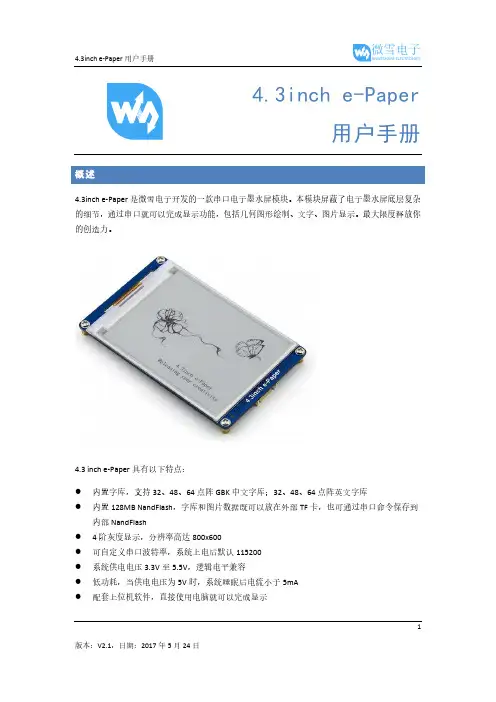
14.3inch e-Paper用户手册4.3inch e-Paper 是微雪电子开发的一款串口电子墨水屏模块。
本模块屏蔽了电子墨水屏底层复杂的细节,通过串口就可以完成显示功能,包括几何图形绘制、文字、图片显示。
最大限度释放你的创造力。
4.3 inch e-Paper 具有以下特点: ● 内置字库,支持32、48、64点阵GBK 中文字库;32、48、64点阵英文字库● 内置128MB NandFlash ,字库和图片数据既可以放在外部TF 卡,也可通过串口命令保存到内部NandFlash● 4阶灰度显示,分辨率高达800x600● 可自定义串口波特率,系统上电后默认115200 ● 系统供电电压3.3V 至5.5V ,逻辑电平兼容● 低功耗,当供电电压为5V 时,系统睡眠后电流小于5mA ●配套上位机软件,直接使用电脑就可以完成显示概述 (1)目录 (2)1.重要提示 (4)2.如何使用 (5)2.1.位图文件的生成 (5)2.2.上位机的使用 (5)2.2.1.硬件连接 (5)2.2.2.安装上位机软件 (5)2.2.3.字库和图片的导入 (7)2.2.4.显示测试 (9)2.3.Arduino (11)2.3.1.硬件连接 (11)2.3.2.程序编译下载 (11)2.4.XNUCLEO-F103RB (11)2.4.1.硬件连接 (11)2.4.2.程序编译下载 (11)2.5.Open103Z (12)2.5.1.硬件连接 (12)2.5.2.程序编译下载 (12)3.串口通信协议 (13)3.1.基本约定 (13)3.1.1.串口说明 (13)23.1.2.指令帧格式 (13)3.1.3.传输顺序 (13)3.1.4.指令参数约定 (13)3.1.5.颜色定义 (13)3.2.指令集 (14)3.2.1.指令速查表 (14)3.2.2.指令详解 (16)4.附录 (21)31.●系统上电系统上电后,会执行一次刷屏操作,将屏幕刷新为白色;如果没有外部TF卡,状态指示灯会闪烁3次并进入常亮;如果有外部TF卡,状态指示灯直接进入常亮。
文档* * 电器制造有限公司产品规格书型号:*****芳香器2007 年 4 月28 日制定[变更履历]本规格书适用于****电器制造有限公司针对出口销售于日本国内100V制造的专用产品芳香器。
2.仕样标准仕样3.外观1)颜色各部件颜色符合表面处理表及限度样板。
2)丝印①不能有批伤、印空、脱落等现象。
②印刷色要符合限度样板。
3)标识①标识内容要明确。
符合图纸。
②在指定位置印刷及贴付。
4)制品批号、个・外装箱批号指定位置要正确、明确地标示出。
5)不能有伤、汚、破裂等。
6)电源线有效长度2.5m±2%4.构造,部品1)组装各部品的组装不能强行压入、接合处、间隙等要根据图面要求。
2)部品各部的部品根据图面或部品承认图。
3)空间距离、沿面距离导电体与其它导电体之间的距离 2.5mm以上导电体非导电体之间的距离 2.0mm以上4)内部配线不能触及可动部、高温部、配线装入时不要过分用力。
5)电装部品①、风扇/马达DFB802024L DC 无刷马达24V 1.9W②、恒温器SS1-L AC 125V 2A 78℃±4℃ (OFF)③、云母发热器100V 20W④、门开关SS-01GL-E欧姆龙微型开关DC 30V 0.1A⑤、齿轮马达开关SS-01-E欧姆龙微型开关DC 30V 0.1A⑥、齿轮马达MT8-4 AC100V 50/60Hz 3/2.5W 2.5/3rpm⑦、热敏电阻150-503-7616 R(25℃)=50KΩ B(25℃/50℃)3,590KΩ(3950 KΩ)⑥、电源线线:PVC线VFF 2×0.75㎟(0.18/30芯)灰色3.1M(有效长)±30mm, JET 2220-12009-1001插头:PP成形插头 JET 0883-43001-1001⑦、主基板环氧树脂CEM-1 电流保险丝AC 125V 1A装倾倒开关⑧、操作基板・遥控基板环氧树脂CEM-1 红外线频率38kHz6)包装符合包装仕样书要求。
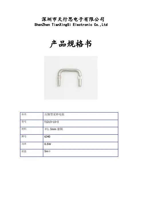
深圳市天行思电子有限公司ShenZhen TianXingSi Electronic Co.,Ltd产品规格书品名压脚型采样电阻型号Y1D15-10-5材料Φ1.5mm康铜牌号6J40功率0.5W阻值5mΩ机械参数元件尺寸(mm)W跨距H标高L脚长10±0.25±0.5 3.5±0.2电气参数项目参数阻值5mΩ±0.125mΩ容通电流10A功率0.5W表面处理无可焊性良好康铜性能项目特点牌号Alloy Name6J40Cu Mn Ni 主要成份Composition%余rem140电阻率ResistivityμΩ·m0.48±0.03电阻温度系数PPM/℃±50对铜热电势EMF VS≤35Cu(0-100℃)uV/℃密度Density g/cm38.9熔点Melting Point℃1280抗拉强度Tensile Strength Mpa>390伸长率%Elongation15-30使用温度Service Temperature0-400规格说明项目规格值试验方法(依据JIS C5202)短时间负荷Within±2%RCWV*2.5or Max OverloadingVoltage,5seconds5Kg/10sec端子强度No evidence ofmechanical damage浸锡试验Within±1%350±10℃,3.5±0.5sAfter test leave for3h260±5℃,10±0.5seconds可焊性试验Covered with new solderby95%at least温度循环试验Within±1%-55~200℃100cycles耐湿负荷试验Within±5%40±2℃,90to95%RH,1000hRated voltage(90min on,30minoff)负荷寿命试验Within±5%70±2℃,1000hRated voltage(90min on,30minoff)用途精度要求±5%范围内的电流采样反馈电路低电感电路大电流脉冲电路包装散装,每包装1000PCS。
文件名称BLU Purchase Specification模组规格书页次1 / 13产品名称215W-3TLED单侧背光版次1.1规格书Specification Sheet 客戶 :(Customer Name) _品名:( Material Name)料号:(Material Number)料号:(Customer Material Number)客户承认CustomerApproved by承认Checked by审核Approved by承认Checked by审核Designed by编写亿科承认AU OPTRONICS CORPORATIONProduct Specification M215HTN01.1() Preliminary Specification(V) Final SpecificationModule 21.5” Color TFT-LCDModel Name M215HTN01.1 open cellCustomer DateApproved byNote: This Specification is subject to change without notice. Approved by Date Howard Lee2012/10/22 Prepared byLouis Jung2012/ 10/22 AU Optronics corporation3.0 Functional Block DiagramThe following diagram shows the functional block of the21.5 inch Color TFT-LCD Module:I/F PCB Interface:P-TWO AL230F-A0G1D-PSTM MSCKT2407P30HBMating Type:FI-X30HL (Locked Type)5.0 Electrical characteristics 5.1 TFT LCD Module 5.1.1 Power SpecificationInput power specifications are as following:Note 1: Measurement conditions:The duration of rising time of power input is 470us.Symbol Parameter Min Typ Max Unit ConditionsVDDLogic/LCD DriveVoltage 4.5 5.0 5.5 [Volt] +/-10%- 1.13 1.36 [A] VDD= 5.0V, All Black Pattern At 60HzIDDInput Current1.34 1.61 [A] VDD= 5.0V, All Black Pattern At 75Hz- 5.65 6.80 [Watt] VDD= 5.0V, All Black Pattern At 60HzPDDVDD Power6.7 8.05 [Watt] VDD= 5.0V, All Black Pattern At 75Hz IRushInrush Current --3[A]Note 1VDDrpAllowable Logic/LCD Drive Ripple Voltage-- 500 [mV] p-pVDD= 5.0V, All Black Pattern At 75Hz6.3 Signal DescriptionPIN # SIGNAL NAME DESCRIPTION1 RxO0- Negat ive LVDS differential data input (Odd data)2 RxO0+ Positive LVDS differential data input (Odd data)3 RxO1- Negat ive LVDS differential data input (Odd data)4 RxO1+ Positive LVDS differential data input (Odd data)5 RxO2- Negat ive LVDS differential data input (Odd data)6 RxO2+ Positive LVDS differential data input (Odd data)7 GND Power Ground8 RxOCLK- Negat ive LVDS differential clock input (O dd clock)9 RxOCLK+ Positive LVDS differential clock input (O dd clock)10 RxO3- Negat ive LVDS differential data input (Odd data)11 RxO3+ Positive LVDS differential data input (Odd data)12 RxE0- Negat ive LVDS differential data input (Even data)13 RxE0+ Positive LVDS differential data input (Even data)14 GND Power Ground15 RxE1- Negat ive LVDS differential data input (Even data)16 RxE1+ Positive LVDS differential data input (Even data)17 GND Power Ground18 RxE2- Negat ive LVDS differential data input (Even data)19 RxE2+ Positive LVDS differential data input (Even data)20 RxECLK- Negat ive LVDS differential clock input (Even clock)21 RxECLK+ Positive LVDS differential clock input (Even clock)22 RxE3- Negat ive LVDS differential data input (Even data)23 RxE3+ Positive LVDS differential data input (Even data)24 GND Power Ground25 NC No connection (for AUO test only. Do not connect)26 NC No connection (for AUO test only. Do not connect)27 NC No connection (for AUO test only. Do not connect)28 VDD Power +5V29 VDD Power +5V30 VDD Power +5VNote 1: Input signals of odd and even clock shall be the same timing.灯条串并定义及接口型号定义:4.. BACKLIGHT UNITValue Parameter Symbol Min. Typ.Max. UnitNote LED Light Bar Input Voltage Per Input PinVPIN -- 56(1), Duty=100%, IPIN=(60mA)IPIN --mA (1), (2) Duty=100%LED Life Time LLED 30000Hrs(3) Power ConsumptionPBL--(9.2)W(1)Duty=100%, IPIN=(60mA)Note (1) LED light bar input voltage and current are measured by utilizing a true RMS multimeter as shownbelow:Note (2) PBL = IPIN × VPINNote (3) The lifetime of LED is defined as the time when LED packages continue to operate under theconditions at Ta = 25 ±2 к and I= (25)mA (per chip) until the brightness becomes Љ 50% of its original value.灯条总电流I230240------V4014(60MA)灯珠 17串4并Figure 1. Measurement Set Up(L =50cm)Figure 2. White Luminance and Uniformity Measurement Locations (9 points) 192 960 17285409727.1.1 Pin AssignmentPin# Signal Name Pin# Signal Name 1 RxO0- 2 RxO0+ 3 RxO1- 4 RxO1+ 5 RxO2- 6 RxO2+ 7 GND 8 RxOCLKIN- 9 RxOCLKIN+ 10 RxO3- 11 RxO3+ 12 RxE0- 13 RxE0+ 14 GND 15 RxE1- 16 RxE1+ 17 GND 18 RxE2- 19 RxE2+ 20 RxECLKIN- 21 RxECLKIN+ 22 RxE3- 23 RxE3+24 GND25NC (for AUO test only. Do not connect)26 NC (for AUO test only. Do not connect) 27 NC (for AUO test only. Do not connect) 28 VDD 29VDD30VDD环境温度(Ta)=25℃±2 湿度HR=65%±10項目 Item單位unit規 格 Spction 备注 RemarkMINTYPMAXCenter point(NOTE 1)1模组亮度BLU BrightnessCenter point cd/m 2250 --- 均匀性Uniformity 9点(NOTE2) 2模组色度LCM CIEx --- -0.030 0.313 +0.030 Center point y --- -0.030 0.329 +0.030Center point中心点为最亮点 The center brightness data ia the maximum下图示中9点之最小数值点比中心点,均匀性定义:Minimum(1-9)/Maximum(5)mum value of 9 point divided by the center ,------75---8.0 Reliability TestEnvironment test conditions are listed as following table.Items Required Condition Note Temperature Humidity Bias (THB) Ta= 50,℃80%RH, 300hoursHigh Temperature Operation (HTO) Ta= 50,℃50%RH, 300hoursLow Temperature Operation (LTO) Ta= 0, 300hours℃High Temperature Storage (HTS) Ta= 60, 300hours℃Low Temperature Storage (LTS) Ta= -20, 300hours℃Vibration Test (Non-operation) Acceleration: 1.5 GrmsWave: RandomFrequency: 10 - 200 HzSweep: 30 Minutes each Axis (X, Y, Z)Shock Test (Non-operation) Acceleration: 50 GWave: Half-sineActive Time: 20 msDirection: ±X,±Y,±Z (one time for each Axis)Drop Test Height: 60 cm, package testThermal Shock Test (TST) -20/℃30min, 60/℃30min, 100 cycles 1 On/Off Test On/10sec, Off/10sec, 30,000 cyclesContact Discharge: ± 15KV, 150pF(330Ω ) 1sec,8 points, 25 times/ point.ESD (Electro Static Discharge)Air Discharge: ± 15KV, 150pF(330Ω ) 1sec8 points, 25 times/ point.2Altitude Test Operation:18,000 ft Non-Operation:40,000 ftNote 1: The TFT-LCD module will not sustain damage after being subjected to 100 cycles of rapid temperature change. A cycle of rapid temperature change consists of varying the temperature from -20℃to 60℃, and back again. Power is not applied during the test. After temperature cycling, the unit is placed in normal room ambient for at least 4 hours before power on.Note 2: EN61000-4-2, ESD class B: Certain performance degradation allowedNo data lostSelf-recoverableNo hardware failures.P。
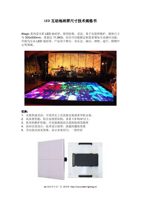
LED互动地砖屏尺寸技术规格书iMagic系列是全彩LED地砖屏,使用轻便,灵活,易于安装和维护。
箱体尺寸为500x500mm,重量仅11.5KG,而且可以根据定制需求增加互动感应功能,升级为互动LED地砖屏,产品用于舞台,音乐会,演出,酒吧,迪厅,购物中心等领域。
优势:1. 安装快速灵活:可采用无工具直接安装或者导轨安装。
2. 高承重性能:铝合金材质结构,承重1.5吨/㎡以上。
3. 优异的维护性能:可直接换取而无需拆除相邻箱体4. 高对比度设计:技术设计面罩,清澈的播放效果5. 杰出低亮高灰效果,显示灰度均匀,一致性好LED互动地砖屏尺寸规格书:像素间距 3.9mm 6.25mm 8.9286mm像素构成SMD 1921 SMD 2727 SMD 3535像素密度65536dot/m2 25600dot/m2 12544dot/m2模组尺寸250×250mm 250×250mm 250×250mm模组分辨率64×64dot 40×40dot 28×28dot箱体尺寸500×500×75mm 500×500×75mm 500×500×75mm 箱体分辨率128×128dot 80×80dot 56×56dot重量11.5kg/Panel 11.5kg/Panel 11.5kg/Panel防护等级IP65/IP43 IP65/IP43 IP65/IP43亮度水平1000~3000CD/m2 1000~3000CD/m2 1000~3000CD/m2 可视角度120°/120°120°/120°120°/120°灰度等级14bit 14bit 14bit最大功率640W/m²620W/m²600W/m²平均功率215W/m²210W/m²200W/m²刷新率≥1920Hz≥1920Hz≥1920Hz输入电源AC110~ 240V, 50/60Hz温度 0°C~40°C(work) , - 20°C~60°C(store)工作寿命≥100,000小时互动感应LED地砖屏,以其压铸铝模块化设计,实现无缝拼接、任意组合,高强度耐磨防滑材料,承重力大,抗冲击力强,紧贴式密闭散热设计,防护等级达IP54,RGB深度灰度处理,实现任意色彩变幻,超大分辨率、超高清晰度和轻薄流畅的外观设计区别于市场上的其他产品,带来的全高清生活体验。
rn6752规格书1.产品概述RN6752是一款高性能的电子产品,主要用于家庭和办公场所。
它具有卓越的性能和强大的功能,为用户提供便捷的使用体验。
2.外观设计RN6752采用时尚的外观设计,整机采用黑色金属材质制作,外观简洁大方。
产品尺寸为XX*XX*XX (单位:毫米),重量为XX克,轻便易携。
3.屏幕和显示RN6752配备XX英寸高清液晶显示屏,分辨率为XXXXxXXXX像素,显示效果清晰逼真。
用户可以根据需要调节亮度和对比度,以适应不同的环境。
4.处理器和内存RN6752搭载XX处理器,主频为XXXGHz,支持快速响应和流畅操作。
内置XXGB RAM和XXGB存储空间,用户可以存储大量的文件和数据。
5.操作系统RN6752使用XX操作系统,界面简洁友好,操作流畅。
用户可以根据个人需求自定义设置,同时支持多任务处理和快速切换。
6.网络和连接RN6752支持WiFi和蓝牙连接,用户可以无线传输和共享数据。
此外,还配备了USB和HDMI接口,方便用户连接外部设备。
7.软件功能RN6752预装了多种实用的软件和应用程序,如日历、闹钟、邮件客户端等。
用户可以根据自己的需求下载和安装更多的应用程序。
8.电池和续航RN6752配备了可拆卸的XXmAh锂电池,续航时间长,可以满足用户一天的正常使用需求。
同时支持快速充电,减少充电时间。
9.摄像头RN6752配备了前置和后置摄像头,前置摄像头像素为XXXX万,可满足用户自拍和视频通话需求。
后置摄像头像素为XXXX万,拍摄效果精美。
10.其他功能RN6752还具有其他实用的功能,如指纹识别、重力感应、陀螺仪等。
这些功能可以提高用户的使用体验,使操作更加方便和安全。
总结:RN6752是一款功能强大、性能优越的电子产品。
它具有出色的外观设计、高清显示屏、快速的处理器和大内存容量。
支持多种连接方式和丰富的软件功能,满足用户的各个需求。
同时拥有长续航时间和优质摄像头,提供更好的使用体验。
fl7102-2q0规格书一、概述:FL7102-2Q0是一款先进的电子产品,具有多种功能和特点。
通过本规格书,我们将为您介绍该产品的详细规格和使用注意事项。
二、外观和尺寸:FL7102-2Q0采用了精致的外观设计,外壳材质为高强度塑料,具有良好的耐久性和抗冲击性能。
尺寸为100毫米×50毫米×10毫米(长×宽×高)。
三、屏幕和显示:FL7102-2Q0配备了高分辨率液晶显示屏,显示画面清晰。
屏幕尺寸为3英寸,可提供良好的视觉效果。
同时,该产品还支持多语言显示,满足不同用户的需求。
四、性能和功能:1.处理器:FL7102-2Q0采用了先进的四核处理器,提供高效的运算性能和处理速度。
2.存储空间:产品内置8GB的闪存,可存储大量数据和文件。
3.电池容量:FL7102-2Q0配备了3000mAh的大容量锂电池,续航时间长,可满足日常使用需求。
4.系统:该产品预装了最新的Android操作系统,用户界面简洁友好,操作方便。
5.网络连接:FL7102-2Q0支持蓝牙和Wi-Fi无线连接,方便用户进行数据传输和上网浏览。
五、摄像和拍照:FL7102-2Q0配备了高清摄像头,具有自动对焦和闪光灯功能。
同时,产品还支持拍照功能,可拍摄清晰的照片。
六、音频和视频播放:该产品支持多种音频和视频格式的播放,用户可以随时欣赏喜爱的音乐和影片。
七、其他特性:1.传感器:FL7102-2Q0内置了加速度传感器和陀螺仪,可实现自动旋转屏幕和游戏体验。
2.输入方式:产品支持触摸屏和虚拟键盘输入,操作简便。
3.存储扩展:FL7102-2Q0支持MicroSD卡的插槽,可扩展存储空间。
4.兼容性:该产品兼容多种应用程序和软件,用户可以自由下载和使用。
八、使用注意事项:为了确保您的安全和正常使用,请在使用前仔细阅读以下注意事项:1.请避免将产品暴露在高温、潮湿或有腐蚀性的环境中。
2.在使用过程中,请勿将产品与水或其他液体接触。
P3室内全彩LED显示屏规格书P3室内全彩LED显示屏特点:1)、系统设计先进合理,显示效果清晰稳定,安装维护方便。
2)、全天候工作:色彩逼真、刷新频率高、防静电、散热效果好、性价比高。
3)、显示方式:左右移动、上下移动、左拉幕、右拉幕、中开合、闪烁、即显等多种方式。
4)、使用节目编辑播放软件,可通过、鼠标编辑、增加、删除和修改文字、图形、图像等信息。
编排的内容存于控制卡,信息播放按节目表自动循环显示。
5)、发光亮度强:发光强度强,并且亮度可调。
6)、视角度好:在水平和垂直均有较大的可视角度,这对水平分布广和高度落差较大的环境均适合。
7)、效果好:采用非线性逐点校正技术,文字更清晰、层次感更强;8)、可靠性强:采用分布式扫描技术和模块化设计技术,可靠性、稳定性更高;9)、显示模式多样化:支持多种显示模式;10)、操作方便:电脑编辑内容发送到系统控制卡,就可显示编辑的内容,系统操作十分方便。
11)、适用范围:商场、企业、学校、舞台、银行、证券、公安、交通、工商、电力、海关、医院、公园、机场、车站、体育场馆等领域室内显示。
P3全彩显示屏技术参数LED屏体波长控制在2.5nm 之内,屏体亮度≥ 1800cd/㎡硬件配置具体特点:(1)、灯管的选用目前国际国内市场上LED灯品种繁多,随着国内芯片技术和封装技术的提高。
如今在世界上著名的有日亚,美国CREE、美国AXT以及台湾光磊、晶元,杭州士兰,三安灯芯等,国内品牌三安,杭州士兰等以其稳定的性能、长寿命低衰减先进的技术在国内广大的显示屏幕生产厂家及最终用户中得到了一致好评,享有极高声誉。
同时他的价格低,性价比高。
我公司P3采用SMD2121黑灯设计,无需面罩,颜色更均匀,高密度像素使画质更清晰视角更宽。
(2)、台湾聚积恒流驱动IC的选用台湾聚积是目前显示屏领域应用最广泛的恒流驱动芯片。
同时它的性能稳定、输出电流通道宽、输出电流值不受负载端电压影响、输出电流值精确度高等特点得到显示屏领域的认可。
psc132压力传感器说明书在使用之前,请安装好LoRa天线,确保电池安装到位,如电池耗尽,请更换同类型的ER14505锂亚电池即可。
锂亚电池电压为3.6V,常规5号南孚电池电压约1.5V,不可替代使用。
如误用,仅无法正常工作,并不会损坏设备。
顶部按键功能长按开机出厂时默认为关机状态,屏幕显示设备ID、芮捷智能官网二维码及软件版本号。
此处二维码可使用SensorTool工具进行自定义修改。
长按按键3s,系统开机,墨水屏有三秒左右刷屏时间,刷屏结束显示当前传感器所读取的气压和温湿度数值,开机完成。
开机画面如下图所示。
除非特殊定制需要,默认设备运行使用LoRaWAN的OTAA方式,设备开机自动入网。
入网完成后自动进行数据采集和上报。
入网成功之前不会上报数据。
非OTAA方式下,设备无入网动作。
长按关机长按按键3s系统关机,墨水屏刷屏,屏幕显示芮捷智能二维码、设备ID编号及频段版本号。
关机之后,不再进行数据采集和上报。
关机画面如下图所示。
关机时屏幕所显示内容可以通过软件自行更改,或与本公司进行沟通代为更改。
在“关机状态”下,短按按键设备并不做任何反馈。
在“开机状态”下,短按按键时,墨水屏开始进行3秒钟的刷屏进行数据更新,刷屏结束,屏幕显示当前传感器获取的气压和温湿度数据,并上报至网关。
显示面板设备正面为2.9寸电子墨水屏,屏幕显示包括气压和温湿度数值、背景Logo图标、设备ID号及ID二维码、剩余电量及使用频段。
当使用LoRaWAN协议时,显示接收信号强度。
开关机显示开机时,显示气压和温湿度数据。
其中背景Logo图片可通过SensorTool工具进行自定义修改。
关机时,屏幕显示二维码、设备版本号信息。
其中二维码可通过SensorTool工具进行自定义修改。
显示电量墨水屏右上角自带电量显示,若电量过低建议更换电池或用外部5V进行供电。
传感器工作指示当传感器进行测量时,电子墨水屏会进行刷屏更新,刷屏时间持续3秒左右。
File Name Specification For HINK 1.5'' EPD Module Number HINK-E0154A09 Version A/0Page Number 1 of 32Specification For HINK 1.5''EPDModel NO.:HINK-E0154A09Product VER:V1.1Customer ApprovalCustomerApproval ByDate Of ApprovalPrepared By Checked By Approval ByHu ting Xiao zhongping Cheng weiHu ziping Jia pengfeiFile Name Specification For HINK 1.5'' EPD Module Number HINK-E0154A09 Version A/0Page Number 2 of 32Version Content Date Producer A/0New release2017/06/26Hu tingFile Name Specification For HINK 1.5'' EPD Module Number HINK-E0154A09 Version A/0Page Number 3 of 32CONTENTS1 General Description ... .......................................................................................................... .42 Features ... ........................................................................................................................... . (4)3 Application ... ......................................................................................................................... ..44 Mechanical Specification ...................................................................................................... ..45 Mechanical Drawing of EPD Module ... ............................................................................. ..56 Input/Output Terminals ... ...................................................................................................... ..67 MCU Interface....................................................................................................................... ..7 7.1 MCU Interface Selection ... ............................................................................................ ..77.2 MCU Serial Peripheral Interface (4-wire SPI) ............................................................. ..77.3 MCU Serial Peripheral Interface (3-wire SPI) .............................................................. ..98 Temperature sensor operation... ............................................................................................. .119 COMMAND TABLE... .......................................................................................................... .1210 Reference Circuit... .............................................................................................................. .1611 Absolute Maximum Rating ... ............................................................................................. .1812 DC Characteristics... ............................................................................................................. .1813 Serial Peripheral Interface Timing... .................................................................................... .1914 Power Consumption... .......................................................................................................... .2015 Typical Operating Sequence................................................................................................ ..2015.1 Normal Operation Flow ... ......................................................................................... ..2015.2 Reference program code ... ....................................................................................... . (21)16 Optical Characteristics... ...................................................................................................... ..2216.1 Specifications ... .......................................................................................................... ..22 16.2 Definition Of Contrast Ratio ... .................................................................................. ..2316.3 Reflection Ratio... ....................................................................................................... ..2317 Handing Safety And Environment Requirements... .......................................................... ..2418 Reliability Test...................................................................................................................... ..2619 Block Diagram... .................................................................................................................. ..27 20PartA/PartB specification .................................................................................................... ..2721 Point And Line Standard... .................................................................................................. ..2822 Barcode. ................................................................................................................................. ..3023 Packing.. ................................................................................................................................ ..31File Name Specification For HINK 1.5'' EPD Module Number HINK-E0154A09 Version A/0Page Number 4 of 321. General DescriptionHINK-E0154A09 is an Active Matrix Electrophoretic Display (AMEPD), with interface and a reference system design. The 1.5” active area contains 152×152 pixels, and has 1-bit B/W full display capabilities. An integrated circuit contains gate buffer, source buffer, interface, timing control logic, oscillator, DC-DC. SRAM.LUT, VCOM and border are supplied with each panel.2. Features●152×152 pixels display●White reflectance above 35%●C ontrast ratio above 10:1●U ltra wide viewing angle●U ltra low power consumption●P ure reflective mode●B i-stable display●C ommercial temperature range●L andscape, portrait modes●H ard-coat antiglare display surface●U ltra Low current deep sleep mode●O n chip display RAM●W aveform stored in On-chip OTP●S erial peripheral interface available●O n-chip oscillator●O n-chip booster and regulator control for generating VCOM, Gate and Source driving voltage●I2C signal master interface to read external temperature sensor/built-in temperature sensor3. ApplicationElectronic Shelf Label System4. Mechanical SpecificationsParameter Specifications Unit RemarkScreen Size 1.5InchDisplay Resolution152(H)×152(V) Pixel Dpi:142Active Area27.00 (H)×27.00 (V) mmPixel Pitch0.177×0.177 mmPixel Configuration SquareOutline Dimension37.32(H)×31.80(V) ×1.05(D) mmWeight 2.1±0.2 gFile Name Specification For HINK 1.5'' EPD Module Number HINK-E0154A09 Version A/0Page Number 5 of 325. Mechanical Drawing of EPD moduleFile Name Specification For HINK 1.5'' EPD Module Number HINK-E0154A09 Version A/0Page Number 6 of 32 6. Input/Output TerminalsPin # Single Description Remark1 NC No connection and do not connect with other NC pins Keep Open2 GDR N-Channel MOSFET Gate Drive Control3 RESE Current Sense Input for the Control Loop4 NC No connection and do not connect with other NC pins e Keep Open5 VSH2 Positive Source driving voltage6 TSCL I2C Interface to digital temperature sensor Clock pin7 TSDA I2C Interface to digital temperature sensor Date pin8 BS1 Bus selection pin Note 6-59 BUSY Busy state output pin Note 6-410 RES # Reset Note 6-311 D/C # Data /Command control pin Note 6-212 CS # Chip Select input pin Note 6-113 SCL serial clock pin (SPI)14 SDA serial data pin (SPI)15 VDDIO Power for interface logic pins16 VCI Power Supply pin for the chip17 VSS Ground18 VDD Core logic power pin19 VPP Power Supply for OTP Programming20 VSH1 Power Supply pin for Positive Gate driving voltage andVSH21 VGH Positive Gate driving voltage22 VSL Negative Source driving voltage23 VGL Power Supply pin for Negative Gate driving voltage,VCOM and VSL24 VCOM VCOM driving voltageFile Name Specification For HINK 1.5'' EPD Module Number HINK-E0154A09 Version A/0Page Number7 of 32Note 6-1: This pin (CS#) is the chip select input connecting to the MCU. The chip is enabled for MCU communication:only when CS# is pulled LOW.Note 6-2: This pin (D/C#) is Data/Command control pin connecting to the MCU. When the pin is pulled HIGH,the data will be interpreted as data. When the pin is pulled LOW, the data will be interpreted as command.Note 6-3: This pin (RES#) is reset signal input. The Reset is active low.Note 6-4: This pin (BUSY) is Busy state output pin. When Busy is High the operation of chip should not beinterrupted and any commands should not be issued to the module. The driver IC will put Busy pin High when thedriver IC is working such as:- Outputting display waveform; or- Communicating with digital temperature sensorNote 6-5: This pin (BS1) is for 3-line SPI or 4-line SPI selection. When it is “Low”, 4-line SPI is selected. When it is “High”, 3-line SPI (9 bits SPI) is selected.7.MCU Interface7.1 MCU interface selectionThe HINK-E0154A09 can support 3-wire/4-wire serial peripheral interface. In the Module, the MCU interface is pin selectable by BS1 pins shown in.T able 7-1: MCU interface selectionBS1 MPU InterfaceL4-lines serial peripheral interface (SPI)H3-lines serial peripheral interface (SPI) - 9 bits SPI7.2 MCU Serial Peripheral Interface (4-wire SPI)The 4-wire SPI consists of serial clock SCL, serial data SDA, D/C# and CS#,The control pins status in 4-wire SPI in writing command/data is shown in Table 7- 2and the write procedure 4-wire SPI is shown in Figue 7-2 Table 7-2 : Control pins status of 4-wire SPIFunction SCL pin SDA pin D/C# pin CS# pinWrite command ↑ Command bit L LWrite data ↑ Data bit H LNote:(1)L is connected to V SS and H is connected to V DDIO(2)↑ stands for rising edge of signalFile Name Specification For HINK 1.5'' EPD Module Number HINK-E0154A09 Version A/0Page Number8 of 32In the write mode, SDA is shifted into an 8-bit shift register on each rising edge of SCL in the order of D7, D6, ...D0. The level of D/C# should be kept over the whole byte. The data byte in the shift register is written to the Graphic Display Data RAM (RAM)/Data Byte register or command Byte register according to D/C# pin.Figure 7-2: Write procedure in 4-wire SPI modeIn the Read mode:1.After driving CS# to low, MCU need to define the register to be read.2.SDA is shifted into an 8-bit shift register on each rising edge of SCL in the order of D7, D6, ... D0 with D/C#keep low.3.After SCL change to low for the last bit of register, D/C# need to drive to high.4.SDA is shifted out an 8-bit data on each falling edge of SCL in the order of D7, D6, 05.Depending on register type, more than 1 byte can be read out. After all byte are read, CS# need to drive to highto stop the read operation.Figure 7-2: Read procedure in 4-wire SPI modeFile Name Specification For HINK 1.5''EPD Module NumberHINK-E0154A09VersionA/0Page Number 9 of 327.3 MCU Serial Peripheral Interface (3-wire SPI)The 3-wire SPI consists of serial clock SCL, serial data SDA and CS#. The operation is similar to 4-wire SPI while D/C# pin is not used and it must be tied to LOW. The control pins status in 3-wire SPI is shown in Table 7-3.Table 7-3 : Control pins status of 3-wire SPI FunctionSCL pin SDA pin D/C# pin CS# pin Write command ↑ Command bit Tie LOW L Write data↑Data bitTie LOWLNote:(1)L is connected to V SS and H is connected to V DDIO (2)↑ stands for rising edge of signalIn the write operation, a 9-bit data will be shifted into the shift register on each clock rising edge. The bit shifting sequence is D/C# bit, D7 bit, D6 bit to D0 bit. The first bit is D/C# bit which determines the following byte is command or data. When D/C# bit is 0, the following byte is command. When D/C# bit is 1, the following byte is data. shows the write procedure in 3-wire SPISCLSDA (Write Mode)D7D6D5D4D3D2D1D0CS#D701Figure 7-3: Write procedure in 3-wire SPI modeFile Name Specification For HINK 1.5'' EPD Module Number HINK-E0154A09 Version A/0Page Number10 of 32In the Read mode:1.After driving CS# to low, MCU need to define the register to be read.2.D/C#=0 is shifted thru SDA with one rising edge of SCL3.SDA is shifted into an 8-bit shift register on each rising edge of SCL in the order of D7, D6, 04.D/C#=1 is shifted thru SDA with one rising edge of SCL5.SDA is shifted out an 8-bit data on each falling edge of SCL in the order of D7, D6, 06.Depending on register type, more than 1 byte can be read out. After all byte are read, CS# need to drive to highto stop the read operation.Figure 7-3: Read procedure in 3-wire SPI modeFile Name Specification For HINK 1.5'' EPD Module Number HINK-E0154A09 Version A/0Page Number11 of 328. Temperature sensor operationFollowing is the way of how to sense the ambient temperature of the module. First, use an external temperature sensor to get the temperature value and converted it into HEX format with below mapping table, then send command 0x1A with the HEX temperature value to the module thru the SPI interface.The temperature value to HEX conversion is as follow:1. If the Temperature value MSByte bit D11 = 0, thenThe temperature is positive and value (DegC) = + (Temperature value) / 162. If the Temperature value MSByte bit D11 = 1, thenThe temperature is negative and value (DegC) = ~ (2’s complement of Temperature value) / 16File Name Specification For HINK 1.5'' EPD Module Number HINK-E0154A09 Version A/0Page Number12 of 329. COMMAND TABLER/W# D/C# Hex D7 D6 D5 D4 D3 D2 D1 D0 Command Description0 0 01 0 0 0 0 0 0 0 1 Driver OutputControl Set the number of gate. Setting for 152 gates is: Set A[8:0] = 97hSet B[7:0] = 00h0 1 - A7A6A5A4A3A2A1A0 0 1 - 0 0 0 0 0 0 0 A8 0 1 - 0 0 0 0 0 B2B1B00 0 03 0 0 0 0 0 0 1 1 Gate DrivingV oltageControl Set Gate driving voltage.A[4:0] = 19h [POR], VGH at 21V0 1 - 0 0 0 A4A3A2A1A00 0 04 0 0 0 0 0 1 0 0 SourceDrivingvoltageControl Set Source output voltage.A[7:0] = 41h [POR], VSH1 at 15V B[7:0] = A8h [POR], VSH2 at 5V C[7:0] = 32h [POR], VSL at -15V0 1 - A7B7C7 A6B6C6A5B5C5A4B4C4A3B3C3A2B2C2A1B1C1A0B0C00 0 10 0 0 0 1 0 0 0 0 Deep SleepMode Deep Sleep mode ControlA[1:0] Description00 Normal Mode [POR]01 Enter Deep Sleep Mode1 11 Enter Deep Sleep Mode20 1 - 0 0 0 0 0 0 A1 A00 0 11 0 0 0 1 0 0 0 1 Data Entrymodesetting Define data entry sequence.A[2:0] = 3h [POR],A [1:0] = ID[1:0]Address automatic increment / decrementsettingThe setting of incrementing or decrementing of the address counter can be made independently in each upper and lower bit of the address.00 –Y decrement, X decrement,01 –Y decrement, X increment,10 –Y increment, X decrement,11 –Y increment, X increment [POR]A[2] = AMSet the direction in which the address counter is updated automatically after data is written to the RAM.When AM= 0, the address counter is updated in the X direction. [POR]When AM = 1, the address counter is updated in the Y direction.0 1 - 0 0 0 0 0 A2A1A00 0 12 0 0 0 1 0 0 1 0 SW RESET It resets the commands and parameters totheir S/W Reset default values exceptR10h-Deep Sleep ModeDuring operation, BUSY pad will output high.Note: RAM are unaffected by this command.0 0 14 0 0 0 1 0 1 0 0 HV ReadyDetectionHV ready detectionThe command required CLKEN=1 andANALOGEN=1Refer to Register 0x22 for detail.After this command initiated, HV Ready detectionstarts.BUSY pad will output high during detection.The detection result can be read from the Status BitRead (Command 0x2F).File Name Specification For HINK 1.5'' EPD Module Number HINK-E0154A09 Version A/0Page Number13 of 32R/W# D/C# Hex D7 D6 D5 D4 D3 D2 D1 D0 Command Description0 0 15 0 0 0 1 0 1 0 1 VCIDetection A[2:0] = 100 [POR] , Detect level at 2.3VA[2:0] : VCI level DetectA[2:0] VCI level011 2.2V100 2.3V101 2.4V110 2.5V111 2.6VOther NAThe command required CLKEN=1 and ANALOGEN=1Refer to Register 0x22 for detail.After this command initiated, VCI detection starts. BUSY pad will output high during detection.The detection result can be read from the Status Bit Read (Command 0x2F).0 1 0 0 0 0 0 A2A1A00 0 1A 0 0 0 1 1 0 1 0 TemperatureSensorControl(Write totemperatureregister) Write to temperature register. A[11:0] =7FFH[POR]0 1 - A11A10A9A8A7A6A5A40 1 - A3A2A1A00 0 0 00 0 20 0 0 1 0 0 0 0 0 MasterActivationActivate Display Update Sequence.The Display Update Sequence Option islocated at R22hBUSY pad will output high during operation.User should not interrupt this operation to avoidcorruption of panel images.0 0 21 0 0 1 0 0 0 0 1 DisplayUpdateControl 1 RAM content option for Display Update A[7:0] = 00h [POR]A[7:4] Red RAM option0000 Normal0100 Bypass RAM content as 0 1000 Inverse RAM contentA[3:0] BW RAM option0000 Normal0100 Bypass RAM content as 0 1000 Inverse RAM content0 1 - A7A6A5A4A3A2A1A00 0 22 0 0 1 0 0 0 1 0 DisplayUpdateControl 2 Display Update Sequence Option:Enable the stage for Master ActivationA[7:0]=FFh (POR)Parameter(in Hex) Enable Clock Signal,Then Enable AnalogThen DISPLAYThen Disable AnalogThen Disable OSCC7Load LUT from OTPEnable Clock Signal,Then Load LUTThen Disable OSC910 1 - A7A6A5A4A3A2A1A00 0 24 0 0 1 0 0 1 0 0 WriteRAM(BW) After this command, data entries will be written into the RAM until another command is written. Address pointers will advance accordingly.For Write pixel:Content of Write RAM(BW)=1For Black pixel:Content of Write RAM( BW)=00 0 26 0 0 1 0 0 1 1 0 WriteRAM(RED) After this command, data entries will be written into the RED RAM until another command is written. Address pointers will advance accordingly. For Red pixel:Content of Write RAM(RED)=1For non-Red pixel[Black or White]:Content of Write RAM(RED)=0File Name Specification For HINK 1.5'' EPD Module Number HINK-E0154A09 Version A/0Page Number14 of 32R/W# D/C# Hex D7 D6 D5 D4 D3 D2 D1 D0 Command Description0 0 2C 0 0 1 0 1 1 0 0 Write VCOMregister Write VCOM register from MCU interfaceA[7:0]=00h[POR]A[7:0] VCOM (V) A[7:0] VCOM (V) 08h -0.2 44h -1.70Bh -0.3 48h -1.810h -0.4 4Bh -1.914h -0.5 50h -217h -0.6 54h -2.11Bh -0.7 58h -2.220h -0.8 5Bh -2.324h -0.9 5Fh -2.428h -1 64h -2.52Ch -1.1 68h -2.62Fh -1.2 6Ch -2.734h -1.3 6Fh -2.837h -1.4 73h -2.93Ch -1.5 78h -340h -1.6 Other NA0 1 - A7A6A5A4A3A2A1A00 0 2D 0 0 1 0 1 1 0 1 OTP RegisterRead Read Register stored in OTP:1. A[7:0]~ B[7:0]: VCOM Information3. C[7:0]~F[7:0]: Reserved4. G[7:0]~H[7:0]: Module ID/ Waveform Version [2bytes]0 1 A7A6A5A4A3A2A1A0…0 1 H7H6H5H4H3H2H1H00 0 2F 0 0 1 0 1 0 0 1 Status Bit Read Read IC status Bit [POR 0x21]A[5]: HV Ready Detection flag [POR=1]0: Ready1: Not ReadyA[4]: VCI Detection flag [POR=0]0: Normal1: VCI lower than the Detect levelA[3]: [POR=0]A[2]: Busy flag [POR=0]0: Normal1: BUSYA[1:0]: Chip ID [POR=01]Remark:A[5] and A[4] status are not valid after RESET, theyneed to be initiated by command 0x14 and command0x15 respectively.1 1 - 0 0 0 A40 0 A1A00 0 32 0 0 1 1 0 0 1 0 Write LUTregister Write LUT register from MCU interface [70 bytes] (excluding the analog setting and frame setting)0 1 - A7A6A5A4A3A2A1A0 0 1 - B7B6B5B4B3B2B1B0 0 1 - : : : : : : : : 0 1 - . . . . . . . .0 0 3A 0 0 1 1 1 0 1 0 Set dummy lineperiod Set A[7:0] = 0Fh0 1 - 0 A6A5A4A3A2A1A00 0 3B 0 0 1 1 1 0 1 1 Set Gate linewidth Set A[3:0] = 0Ch0 1 - 0 0 0 0 A3A2A1A0File Name Specification For HINK 1.5'' EPD Module Number HINK-E0154A09 Version A/0Page Number15 of 32R/W# D/C# Hex D7 D6 D5 D4 D3 D2 D1 D0 Command Description0 0 3C 0 0 1 1 1 1 0 0 BorderWaveformControl Select border waveform for VBDA [7:6] Select VBDA[7:6] Select VBD as00[POR] GS Transition DefineA[1:0]01 Fix Level Define A[5:4]10 VCOM11 HIZA [5:4] Fix Level Setting for VBDA[5:4] VBD level00[POR] VSS01 VSH110 VSL11 VSH2A[1:0]) GS Transition setting for VBDA[1:0] VBD Transition00 [POR] LUT001 LUT110 LUT211 LUT30 1 - A7A6A5A40 0 A1A00 0 44 0 1 0 0 0 1 0 0 Set RAM X -addressStart / Endposition Specify the start/end positions of the window address in the X direction by an address unitA[4:0]: X-Start, POR = 00hB[4:0]: X-End, POR = 12h0 1 - 0 0 0 A4A3A2A1A0 0 1 - 0 0 0 B4B3B2B1B00 0 45 0 1 0 0 0 1 0 1 Set Ram Y-addressStart / Endposition Specify the start/end positions of the window address in the Y direction by an address unitA[7:0]: Y-Start, POR = 00hB[7:0]: Y-End, POR = F9h0 1 - A7A6A5A4A3A2A1A0 0 1 0 0 0 0 0 0 0 A8 0 1 - B7B6B5B4B3B2B1B0 0 1 0 0 0 0 0 0 0 B80 0 4E 0 1 0 0 1 1 1 0 Set RAM X -addresscounter Make initial settings for the RAM X address in the address counter (AC) A[4:0] : POR is 00h0 1 - 0 0 0 A4A3A2A1A00 0 4F 0 1 0 0 1 1 1 1 Set RAM Y -addresscounter Make initial settings for the RAM Y address in the address counter (AC) A[7:0] : POR is 00h0 1 - A7A6A5A4A3A2A1A00 0 0 0 0 0 0 A80 0 74 0 1 1 1 0 1 0 0 Set AnalogBlockcontrol A[7:0] = 54h0 1 A7A6A5A4A3A2A1A00 0 7E 0 1 1 1 1 1 1 0 Set DigitalBlockcontrol A[7:0] = 3Bh0 1 A7A6A5A4A3A2A1A0File Name Specification For HINK 1.5'' EPD Module Number HINK-E0154A09 Version A/0Page Number16 of 3210.Reference CircuitFigure. 10-1File Name Specification For HINK 1.5'' EPD Module Number HINK-E0154A09 Version A/0Page Number17 of 32Figure. 10-2File Name Specification For HINK 1.5'' EPD Module Number HINK-E0154A09 Version A/0Page Number18 of 3211. ABSOLUTE MAXIMUM RATINGT able 11-1: Maximum RatingsSymbol Parameter Rating UnitV CI Logic supply voltage -0.5 to +6.0 VT OPR Operation temperature range 0 to 50 °CT STG Storage temperature range -25 to 60 °C12.DC CHARACTERISTICSThe following specifications apply for: VSS=0V, VCI=3.3V, T OPR=25℃.Table 12-1: DC CharacteristicsSymbol Parameter T est Condition Applicable pin Min. Typ. Max. Unit VCI VCI operation voltage - VCI 2.2 3.3 3.7 VVIH High level input voltage - SDA, SCL, CS#,D/C#, RES#, 0.8VDDIO- - VVIL Low level input voltage - - - 0.2VDDIOVVOH High level output voltage IOH = -100uA BUSY 0.9VDDIO- - VVOL Low level output voltage IOL = 100uA - - 0.1VDDIOV Iupdate Module operating current- - - 3 - mA Isleep Deep sleep mode VCI=3.3V- - 0.6 1 uA - The Typical power consumption is measured using associated 25℃ waveform with followingpattern transition: from horizontal scan pattern to vertical scan pattern. (Note 12-1)- The listed electrical/optical characteristics are only guaranteed under the controller &waveform provided by XingTai.- Vcom value will be OTP before in factory or present on the label sticker.N ote 12-1The Typical power consumptionFile Name Specification For HINK 1.5'' EPD Module Number HINK-E0154A09 Version A/0Page Number19 of 3213. Serial Peripheral Interface TimingThe following specifications apply for: VSS=0V, VCI=2.2V to 3.7V, T OPR=25℃Write modeSymbol Parameter Min Typ Max Unit fSCL SCL frequency (Write Mode) 20 MHz tCSSU Time CS# has to be low before the first rising edge of SCLK 20 ns tCSHLD Time CS# has to remain low after the last falling edge of SCLK 20 ns tCSHIGH Time CS# has to remain high between two transfers 100 ns tSCLHIGH Part of the clock period where SCL has to remain high 25 ns tSCLLOW Part of the clock period where SCL has to remain low 25 ns tSISU Time SI (SDA Write Mode) has to be stable before the next rising edge of SCL 10 ns tSIHLD Time SI (SDA Write Mode) has to remain stable after the rising edge of SCL 40 ns Read modeSymbol Parameter Min Typ Max Unit fSCL SCL frequency (Read Mode) 2.5 MHz tCSSU Time CS# has to be low before the first rising edge of SCLK 100 ns tCSHLD Time CS# has to remain low after the last falling edge of SCLK 50 ns tCSHIGH Time CS# has to remain high between two transfers 250 ns tSCLHIGH Part of the clock period where SCL has to remain high 180 ns tSCLLOW Part of the clock period where SCL has to remain low 180 ns tSOSU Time SO(SDA Read Mode) will be stable before the next rising edge of SCL 50 ns tSOHLD Time SO (SDA Read Mode) will remain stable after the falling edge of SCL 0 ns Note: All timings are based on 20% to 80% of VDDIO-VSSFigure 13-1 : Serial peripheral interface characteristics14 .Power ConsumptionParameter Symbol Conditions TYP Max Unit Remark Panel power consumption during update - 25℃ 5.8 - mAs - Deep sleep mode - 25℃0.6 - uA -File Name Specification For HINK 1.5'' EPD Module Number HINK-E0154A09Version A/0Page Number20 of 3215. Typical Operating Sequence 15.1 Normal Operation FlowFile Name Specification For HINK 1.5'' EPD Module Number HINK-E0154A09 Version A/0Page Number21 of 3215.2 Reference Program CodeFile Name Specification For HINK 1.5'' EPD Module Number HINK-E0154A09 Version A/0Page Number22 of 3216. Optical characteristics16.1 SpecificationsMeasurements are made with that the illumination is under an angle of 45 degrees, the detection is perpendicular unless otherwise specified.T=25℃SYMBOL PARAMETER CONDITIONSMIN TYPE MAX UNIT NoteR Reflectance White 30 35 - % Note 16-1 Gn 2Grey Level - - DS+(WS-DS)×n(m-1) - L* - CR Contrast Ratio indoor - 10 - - - Panel’s life- 0℃~50℃5years or 1000000 times - - Note 16-2WS: White state, DS : Dark statem: 2Note 16-1: Luminance meter : Eye - One Pro SpectrophotometerNote 16-2: We guarantee display quality from 0℃~30℃ generally,If operation ambient temperature from 30~50℃,will Offer special waveform by Xingtai.File Name Specification For HINK 1.5'' EPD Module Number HINK-E0154A09 Version A/0Page Number23 of 3216.2 Definition of contrast ratioThe contrast ratio (CR) is the ratio between the reflectance in a full white area (R1) and the reflectance in a dark area (Rd)() :R1: white reflectance Rd: dark reflectanceCR = R1/Rd16.3 Reflection RatioThe reflection ratio is expressed as :R = Reflectance Factor white board x (L center / L white board )L center is the luminance measured at center in a white area (R=G =B=1) . L white board is the luminance of a standard white board . Both are measured with equivalent illumination source . The viewing angle shall be no more than 2 degrees .File Name Specification For HINK 1.5'' EPD Module Number HINK-E0154A09 Version A/0Page Number24 of 3217. HANDLING,SAFETY AND ENVIROMENTAL REQUIREMENTSW ARNINGThe display glass may break when it is dropped or bumped on a hard surface. Handle with care. Should the display break, do not touch the electrophoretic material. In case of contact with electrophoretic material, wash with water and soap.CAUTIONThe display module should not be exposed to harmful gases, such as acid and alkali gases, which corrode electronic components.Disassembling the display module can cause permanent damage and invalidate the warranty agreements.IPA solvent can only be applied on active area and the back of a glass. For the rest part, it is not allowed.Observe general precautions that are common to handling delicate electronic components. The glass can break andfront surfaces can easily be damaged . Moreover the display is sensitive to static electricity and other roughenvironmental conditions.Mounting Precautions(1) It`s recommended that you consider the mounting structure so that uneven force (ex. Twisted stress) is not applied tothe module.(2) It`s recommended that you attach a transparent protective plate to the surface in order to protect the EPD.Transparent protective plate should have sufficient strength in order to resist external force.(3) You should adopt radiation structure to satisfy the temperature specification.(4) Acetic acid type and chlorine type materials for the cover case are not desirable because the former generatescorrosive gas of attacking the PS at high temperature and the latter causes circuit break by electro-chemical reaction.(5) Do not touch, push or rub the exposed PS with glass, tweezers or anything harder than HB pencil lead. And please donot rub with dust clothes with chemical treatment. Do not touch the surface of PS for bare hand or greasy cloth. (Some cosmetics deteriorate the PS)(6) When the surface becomes dusty, please wipe gently with absorbent cotton or other soft materials like chamois soakswith petroleum benzene. Normal-hexane is recommended for cleaning the adhesives used to attach the PS. Do not use acetone, toluene and alcohol because they cause chemical damage to the PS.(7) Wipe off saliva or water drops as soon as possible. Their long time contact with PS causes deformations and colorfading.Product specification The data sheet contains final product specifications.。