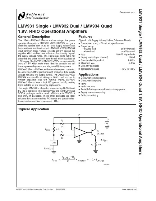
LMV931Single /LMV932Dual /LMV934Quad 1.8V,RRIO Operational AmplifiersGeneral DescriptionThe LMV931/LMV932/LMV934are low voltage,low power operational amplifiers.LMV931/LMV932/LMV934are guar-anteed to operate from +1.8V to +5.0V supply voltages and have rail-to-rail input and output.LMV931/LMV932/LMV934input common mode voltage extends 200mV beyond the supplies which enables user enhanced functionality beyond the supply voltage range.The output can swing rail-to-rail unloaded and within 105mV from the rail with 600Ωload at 1.8V supply.The LMV931/LMV932/LMV934are optimized to work at 1.8V which make them ideal for portable two-cell battery powered systems and single cell Li-Ion systems.LMV931/LMV932/LMV934exhibit excellent speed-power ra-tio,achieving 1.4MHz gain bandwidth product at 1.8V supply voltage with very low supply current.The LMV931/LMV932/LMV934are capable of driving a 600Ωload and up to 1000pF capacitive load with minimal ringing.LMV931/LMV932/LMV934have a high DC gain of 101dB,making them suitable for low frequency applications.The single LMV931is offered in space saving SC70-5and SOT23-5packages.The dual LMV932are in MSOP-8and SOIC-8packages and the quad LMV934are in TSSOP-14and SOIC-14packages.These small packages are ideal solutions for area constrained PC boards and portable elec-tronics such as cellular phones and PDAs.Features(Typical 1.8V Supply Values;Unless Otherwise Noted)n Guaranteed 1.8V,2.7V and 5V specifications n Output swing —w/600Ωload 80mV from rail —w/2k Ωload 30mV from rail n V CM 200mV beyond rails n Supply current (per channel)100µA n Gain bandwidth product 1.4MHz n Maximum V OS 4.0mV n Ultra tiny packages n Temperature range −40˚C to 125˚CApplicationsn Consumer communication n Consumer computing n PDAsn Audio pre-ampn Portable/battery-powered electronic equipment n Supply current monitoring nBattery monitoringTypical Application200326H0December 2002LMV931Single /LMV932Dual /LMV934Quad 1.8V,RRIO Operational Amplifiers©2002National Semiconductor Corporation Absolute Maximum Ratings(Note 1)If Military/Aerospace specified devices are required,please contact the National Semiconductor Sales Office/Distributors for availability and specifications.ESD Tolerance (Note 2)Machine Model 200V Human Body Model 2000VDifferential Input Voltage ±Supply VoltageSupply Voltage (V +–V −)5.5VOutput Short Circuit to V +(Note 3)Output Short Circuit to V −(Note 3)Storage Temperature Range −65˚C to 150˚CJunction Temperature (Note 4)150˚C Mounting Temp.Infrared or Convection (20sec)235˚COperating Ratings (Note 1)Supply Voltage Range 1.8V to 5.0V Temperature Range −40˚C to 125˚CThermal Resistance (θJA )SC70-5414˚C/W SOT23-5265˚C/W MSOP-8235˚C/W SOIC-8175˚C/W TSSOP-14155˚C/W SOIC-14127˚C/W 1.8V DC Electrical CharacteristicsUnless otherwise specified,all limits guaranteed for T J =25˚C.V +=1.8V,V −=0V,V CM =V +/2,V O =V +/2and R L >1M Ω.Boldface limits apply at the temperature extremes.See (Note 10)Symbol ParameterConditionMin (Note 6)Typ (Note 5)Max (Note 6)Units V OSInput Offset VoltageLMV931(Single)146mV LMV932(Dual)LMV934(Quad)1 5.57.5mV TCV OS Input Offset Voltage Average Drift5.5µV/˚C I B Input Bias Current 153550nA I OS Input Offset Current132540nAI S Supply Current (per channel)103185205µACMRRCommon Mode Rejection RatioLMV931,0≤V CM ≤0.6V 1.4V ≤V CM ≤1.8V (Note 8)605578dBLMV932and LMV9340≤V CM ≤0.6V1.4V ≤V CM ≤1.8V (Note 8)555076−0.2V ≤V CM ≤0V 1.8V ≤V CM ≤2.0V5072PSRR Power Supply Rejection Ratio1.8V ≤V +≤5V 7570100dBCMVRInput Common-Mode Voltage RangeFor CMRR Range ≥50dBT A =25˚C V −−0.2−0.2to 2.1V ++0.2V T A −40˚C to 85˚C V −V +T A =125˚CV −+0.2V +−0.2A VLarge Signal Voltage Gain LMV931(Single)R L =600Ωto 0.9V,V O =0.2V to 1.6V,V CM =0.5V 7773101dBR L =2k Ωto 0.9V,V O =0.2V to 1.6V,V CM =0.5V8075105Large Signal Voltage Gain LMV932(Dual)LMV934(Quad)R L =600Ωto 0.9V,V O =0.2V to 1.6V,V CM =0.5V 757290dB R L =2k Ωto 0.9V,V O =0.2V to 1.6V,V CM =0.5V7875100L M V 931S i n g l e /L M V 932D u a l /L M V 934Q u a d 21.8V DC Electrical Characteristics(Continued)Unless otherwise specified,all limits guaranteed for T J =25˚C.V +=1.8V,V −=0V,V CM =V +/2,V O =V +/2and R L >1M Ω.Boldface limits apply at the temperature extremes.See (Note 10)Symbol ParameterConditionMin (Note 6)Typ (Note 5)Max (Note 6)UnitsV OOutput SwingR L =600Ωto 0.9V V IN =±100mV1.651.631.72V0.0770.1050.120R L =2k Ωto 0.9V V IN =±100mV1.751.741.770.0240.0350.04I OOutput Short Circuit CurrentSourcing,V O =0V V IN =100mV 43.38mASinking,V O =1.8V V IN =−100mV7591.8V AC Electrical CharacteristicsUnless otherwise specified,all limits guaranteed for T J =25˚C.V +=1.8V,V −=0V,V CM =V +/2,V O =V +/2and R L >1M Ω.Boldface limits apply at the temperature extremes.See (Note 10)Symbol ParameterConditionsMin (Note 6)Typ (Note 5)Max (Note 6)Units SR Slew Rate(Note 7)0.35V/µs GBW Gain-Bandwidth Product 1.4MHz Φm Phase Margin 67deg G m Gain Margin7dBe n Input-Referred Voltage Noisef =1kHz,V CM =0.5V 60i n Input-Referred Current Noise f =1kHz0.06THDTotal Harmonic Distortion f =1kHz,A V =+1R L =600Ω,V IN =1V PP 0.023%Amp-to-Amp Isolation(Note 9)123dB2.7V DC Electrical CharacteristicsUnless otherwise specified,all limits guaranteed for T J =25˚C.V +=2.7V,V −=0V,V CM =V +/2,V O =V +/2and R L >1M Ω.Boldface limits apply at the temperature extremes.See (Note 10)Symbol ParameterConditionMin (Note 6)Typ (Note 5)Max (Note 6)Units V OSInput Offset VoltageLMV931(Single)146mV LMV932(Dual)LMV934(Quad)1 5.57.5mV TCV OS Input Offset Voltage Average Drift5.5µV/˚C I B Input Bias Current 153550nA I OS Input Offset Current82540nAI SSupply Current (per channel)105190210µALMV931Single /LMV932Dual /LMV934Quad32.7V DC Electrical Characteristics(Continued)Unless otherwise specified,all limits guaranteed for T J =25˚C.V +=2.7V,V −=0V,V CM =V +/2,V O =V +/2and R L >1M Ω.Boldface limits apply at the temperature extremes.See (Note 10)Symbol ParameterConditionMin (Note 6)Typ (Note 5)Max (Note 6)UnitsCMRRCommon Mode Rejection RatioLMV931,0≤V CM ≤1.5V 2.3V ≤V CM ≤2.7V (Note 8)605581dBLMV932and LMV9340≤V CM ≤1.5V2.3V ≤V CM ≤2.7V (Note 8)555080−0.2V ≤V CM ≤0V 2.7V ≤V CM ≤2.9V5074PSRR Power Supply Rejection Ratio1.8V ≤V +≤5V V CM =0.5V7570100dBV CMInput Common-Mode Voltage Range For CMRR Range ≥50dBT A =25˚C V −−0.2−0.2to 3.0V ++0.2V T A =−40˚C to 85˚C V −V +T A =125˚CV −+0.2V +−0.2A VLarge Signal Voltage Gain LMV931(Single)R L =600Ωto 1.35V,V O =0.2V to 2.5V 8786104dBR L =2k Ωto 1.35V,V O =0.2V to 2.5V9291110Large Signal Voltage Gain LMV932(Dual)LMV934(Quad)R L =600Ωto 1.35V,V O =0.2V to 2.5V 787590dB R L =2k Ωto 1.35V,V O =0.2V to 2.5V 8178100V OOutput SwingR L =600Ωto 1.35V V IN =±100mV2.552.532.62V0.0830.1100.130R L =2k Ωto 1.35V V IN =±100mV2.652.642.6750.0250.040.045I OOutput Short Circuit CurrentSourcing,V O =0V V IN =100mV 201530mASinking,V O =0V V IN =−100mV1812252.7V AC Electrical CharacteristicsUnless otherwise specified,all limits guaranteed for T J =25˚C.V +=2.7V,V −=0V,V CM =1.0V,V O =1.35V and R L >1M Ω.Boldface limits apply at the temperature extremes.See (Note 10)Symbol ParameterConditionsMin (Note 6)Typ (Note 5)Max (Note 6)Units SR Slew Rate(Note 7)0.4V/µs GBW Gain-Bandwidth Product 1.4MHz Φm Phase Margin 70deg G m Gain Margin7.5dBe n Input-Referred Voltage Noisef =1kHz,V CM =0.5V 57i nInput-Referred Current Noisef =1kHz 0.082L M V 931S i n g l e /L M V 932D u a l /L M V 934Q u a d 42.7V AC Electrical Characteristics(Continued)Unless otherwise specified,all limits guaranteed for T J=25˚C.V+=2.7V,V−=0V,V CM=1.0V,V O=1.35V and R L>1MΩ.Boldface limits apply at the temperature extremes.See(Note10)Symbol Parameter Conditions Min(Note6)Typ(Note5)Max(Note6)UnitsTHD Total Harmonic Distortion f=1kHz,A V=+1R L=600kΩ,V IN=1V PP0.022%Amp-to-Amp Isolation(Note9)123dB 5V DC Electrical CharacteristicsUnless otherwise specified,all limits guaranteed for T J=25˚C.V+=5V,V−=0V,V CM=V+/2,V O=V+/2andR L>1MΩ.Boldface limits apply at the temperature extremes.See(Note10)Symbol Parameter Condition Min(Note6)Typ(Note5)Max(Note6)UnitsV OS Input Offset Voltage LMV931(Single)146mVLMV932(Dual) LMV934(Quad)1 5.57.5mVTCV OS Input Offset Voltage AverageDrift5.5µV/˚CI B Input Bias Current143550nAI OS Input Offset Current92540nAI S Supply Current(per channel)116210230µACMRR Common Mode RejectionRatio 0≤V CM≤3.8V4.6V≤V CM≤5.0V(Note8)605586dB −0.2V≤V CM≤0V5.0V≤V CM≤5.2V5078PSRR Power Supply RejectionRatio 1.8V≤V+≤5VV CM=0.5V7570100dBCMVR Input Common-Mode VoltageRange For CMRRRange≥50dBT A=25˚C V−−0.2−0.2to5.3V++0.2V T A=−40˚C to85˚CV−V+T A=125˚C V−+0.3V+−0.3A V Large Signal Voltage GainLMV931(Single)R L=600Ωto2.5V,V O=0.2V to4.8V8887102dB R L=2kΩto2.5V,V O=0.2V to4.8V9493113Large Signal Voltage Gain LMV932(Dual)LMV934(Quad)R L=600Ωto2.5V,V O=0.2V to4.8V817890dB R L=2kΩto2.5V,V O=0.2V to4.8V8582100V O Output Swing R L=600Ωto2.5VV IN=±100mV 4.8554.8354.890V0.1200.1600.180R L=2kΩto2.5V V IN=±100mV4.9454.9354.9670.0370.0650.075LMV931Single/LMV932Dual/LMV934Quad55V DC Electrical Characteristics(Continued)Unless otherwise specified,all limits guaranteed for T J =25˚C.V +=5V,V −=0V,V CM =V +/2,V O =V +/2and R L >1M Ω.Boldface limits apply at the temperature extremes.See (Note 10)Symbol ParameterConditionMin (Note 6)Typ (Note 5)Max (Note 6)UnitsI OOutput Short Circuit CurrentLMV931,Sourcing,V O =0V V IN =100mV 8068100mASinking,V O =5V V IN =−100mV5845655V AC Electrical CharacteristicsUnless otherwise specified,all limits guaranteed for T J =25˚C.V +=5V,V −=0V,V CM =V +/2,V O =2.5V and R L >1M Ω.Boldface limits apply at the temperature extremes.See (Note 10)Symbol ParameterConditionsMin (Note 6)Typ (Note 5)Max (Note 6)Units SR Slew Rate(Note 7)0.42V/µs GBW Gain-Bandwidth Product 1.5MHz Φm Phase Margin 71deg G m Gain Margin8dBe n Input-Referred Voltage Noisef =1kHz,V CM =1V 50i n Input-Referred Current Noise f =1kHz0.07THDTotal Harmonic Distortion f =1kHz,A V =+1R L =600Ω,V O =1V PP0.022%Amp-to-Amp Isolation(Note 9)123dBNote 1:Absolute Maximum Ratings indicate limits beyond which damage to the device may occur.Operating Ratings indicate conditions for which the device is intended to be functional,but specific performance is not guaranteed.For guaranteed specifications and the test conditions,see the Electrical Characteristics.Note 2:Human body model,1.5k Ωin series with 100pF.Machine model,200Ωin series with 100pF.Note 3:Applies to both single-supply and split-supply operation.Continuous short circuit operation at elevated ambient temperature can result in exceeding the maximum allowed junction temperature of 150˚C.Output currents in excess of 45mA over long term may adversely affect reliability.Note 4:The maximum power dissipation is a function of T J(MAX),θJA ,and T A .The maximum allowable power dissipation at any ambient temperature is P D =(T J(MAX)–T A )/θJA .All numbers apply for packages soldered directly into a PC board.Note 5:Typical Values represent the most likely parametric norm.Note 6:All limits are guaranteed by testing or statistical analysis.Note 7:V +=5V.Connected as voltage follower with 5V step input.Number specified is the slower of the positive and negative slew rates.Note 8:For guaranteed temperature ranges,see Input Common-Mode Voltage Range specifications.Note 9:Input referred,V +=5V and R L =100k Ωconnected to 2.5V.Each amp excited in turn with 1kHz to produce V O =3V PP .Note 10:Electrical Table values apply only for factory testing conditions at the temperature indicated.Factory testing conditions result in very limited self-heating of the device such that T J =T A .No guarantee of parametric performance is indicated in the electrical tables under conditions of internal self-heating where T J >T A .See Applications section for information of temperature derating of the device.Absolute Maximum Ratings indicated junction temperature limits beyond which the device may be permanently degraded,either mechanically or electrically.L M V 931S i n g l e /L M V 932D u a l /L M V 934Q u a d 6Connection Diagrams5-Pin SC70-5/SOT23-5(LMV931)8-Pin MSOP/SOIC(LMV932)14-Pin TSSOP/SOIC(LMV934)200326AO Top View200326G12 Top View200326G13 Top ViewOrdering InformationPackage Part Number Packaging Marking Transport Media NSCDrawing5-Pin SC70LMV931MGA741k Units Tape and ReelMAA05A LMV931MGX3k Units Tape and Reel5-Pin SOT23LMV931MFA79A1k Units Tape and ReelMF05A LMV931MFX3k Units Tape and Reel8-Pin MSOPLMV932MMA86A1k Units Tape and ReelMUA08A LMV932MMX 3.5k Units Tape and Reel8-Pin SOICLMV932MALMV932MARailsM08A LMV932MAX 2.5k Units Tape and Reel14-Pin TSSOPLMV934MTLMV934MTRailsMTC14 LMV934MTX 2.5k Units Tape and Reel14-Pin SOICLMV934MALMV934MARailsM14ALMV934MAX 2.5k Units Tape and ReelLMV931Single/LMV932Dual/LMV934Quad7Typical Performance CharacteristicsUnless otherwise specified,V S =+5V,single supply,T A =25˚C.Supply Current vs.Supply Voltage (LMV931)Sourcing Current vs.Output Voltage2003262220032625Sinking Current vs.Output Voltage Output Voltage Swing vs.Supply Voltage2003262820032649Output Voltage Swing vs.Supply Voltage Gain and Phase vs.Frequency20032650200326G8L M V 931S i n g l e /L M V 932D u a l /L M V 934Q u a d 8Typical Performance Characteristics Unless otherwise specified,V S =+5V,single supply,T A =25˚C.(Continued)Gain and Phase vs.FrequencyGain and Phase vs.Frequency200326G9200326G10Gain and Phase vs.Frequency CMRR vs.Frequency200326G1120032639PSRR vs.Frequency Input Voltage Noise vs.Frequency2003265620032658LMV931Single /LMV932Dual /LMV934Quad9Typical Performance Characteristics Unless otherwise specified,V S =+5V,single supply,T A =25˚C.(Continued)Input Current Noise vs.FrequencyTHD vs.Frequency2003266620032667THD vs.Frequency Slew Rate vs.Supply Voltage2003266820032669Small Signal Non-Inverting Response Small Signal Non-Inverting Response2003267020032671L M V 931S i n g l e /L M V 932D u a l /L M V 934Q u a d 10Typical Performance Characteristics Unless otherwise specified,V S =+5V,single supply,T A =25˚C.(Continued)Small Signal Non-Inverting ResponseLarge Signal Non-Inverting Response2003267220032673Large Signal Non-Inverting Response Large Signal Non-Inverting Response2003267420032675Short Circuit Current vs.Temperature (Sinking)Short Circuit Current vs.Temperature (Sourcing)2003267620032677LMV931Single /LMV932Dual /LMV934Quad11Typical Performance Characteristics Unless otherwise specified,V S =+5V,single supply,T A =25˚C.(Continued)Offset Voltage mon Mode RangeOffset Voltage mon Mode Range2003263620032637Offset Voltage mon Mode Range20032638L M V 931S i n g l e /L M V 932D u a l /L M V 934Q u a d 12Application Note1.0INPUT AND OUTPUT STAGEThe rail-to-rail input stage of this family provides more flex-ibility for the designer.The LMV931/LMV932/LMV934use a complimentary PNP and NPN input stage in which the PNP stage senses common mode voltage near V−and the NPN stage senses common mode voltage near V+.The transition from the PNP stage to NPN stage occurs1V below V+.Since both input stages have their own offset voltage,the offset of the amplifier becomes a function of the input common mode voltage and has a crossover point at1V below V+.This V OS crossover point can create problems for both DC and AC coupled signals if proper care is not rge input signals that include the V OS crossover point will cause distortion in the output signal.One way to avoid such distor-tion is to keep the signal away from the crossover.For example,in a unity gain buffer configuration and with V S= 5V,a5V peak-to-peak signal will contain input-crossover distortion while a3V peak-to-peak signal centered at1.5V will not contain input-crossover distortion as it avoids the crossover point.Another way to avoid large signal distortion is to use a gain of−1circuit which avoids any voltage excursions at the input terminals of the amplifier.In that circuit,the common mode DC voltage can be set at a level away from the V OS cross-over point.For small signals,this transition in V OS shows up as a V CM dependent spurious signal in series with the input signal and can effectively degrade small signal parameters such as gain and common mode rejection ratio.To resolve this problem,the small signal should be placed such that it avoids the V OS cross-over point.In addition to the rail-to-rail performance,the output stage can provide enough output current to drive 600Ωloads.Because of the high current capability,care should be taken not to exceed the150˚C maximum junction temperature specification.2.0INPUT BIAS CURRENT CONSIDERATIONThe LMV931/LMV932/LMV934family has a complementary bipolar input stage.The typical input bias current(I B)is 15nA.The input bias current can develop a significant offset voltage.This offset is primarily due to I B flowing through the negative feedback resistor,R F.For example,if I B is50nA and R F is100kΩ,then an offset voltage of5mV will develop (V OS=I B x R F).Using a compensation resistor(R C),as shown in Figure1,cancels this effect.But the input offset current(I OS)will still contribute to an offset voltage in the same manner.Typical Applications3.0HIGH SIDE CURRENT SENSINGThe high side current sensing circuit(Figure2)is commonlyused in a battery charger to monitor charging current toprevent over charging.A sense resistor R SENSE is connectedto the battery directly.This system requires an op amp withrail-to-rail input.The LMV931/LMV932/LMV934are ideal forthis application because its common mode input range goesup to the rail.20032659FIGURE1.Canceling the Offset Voltage due to InputBias Current200326H0FIGURE2.High Side Current SensingLMV931Single/LMV932Dual/LMV934Quad13Typical Applications(Continued)4.0HALF-WAVE RECTIFIER WITH RAIL-TO-GROUND OUTPUT SWINGSince the LMV931/LMV932/LMV934input common mode range includes both positive and negative supply rails and the output can also swing to either supply,achieving half-wave rectifier functions in either direction is an easy task.All that is needed are two external resistors;there is no need for diodes or matched resistors.The half wave rectifier can have either positive or negative going outputs,depending on the way the circuit is arranged.In Figure 3the circuit is referenced to ground,while in Figure 4the circuit is biased to the positive supply.These configu-rations implement the half wave rectifier since the LMV931/LMV932/LMV934can not respond to one-half of the incom-ing waveform.It can not respond to one-half of the incoming because the amplifier can not swing the output beyond either rail therefore the output disengages during this half cycle.During the other half cycle,however,the amplifier achieves a half wave that can have a peak equal to the total supply voltage.R I should be large enough not to load the LMV931/LMV932/LMV934.5.0INSTRUMENTATION AMPLIFIER WITH RAIL-TO-RAIL INPUT AND OUTPUTSome manufactures make a non-“rail-to-rail”-op amp rail-to-rail by using a resistive divider on the inputs.The resistors divide the input voltage to get a rail-to-rail input range.The problem with this method is that it also divides the signal,so in order to get the obtained gain,the amplifier must have a higher closed loop gain.This raises the noise and drift by the internal gain factor and lowers the input impedance.Any mismatch in these precision resistors reduces the CMRR as well.The LMV981/LMV982is rail-to-rail and therefore doesn’t have these disadvantages.Using three of the LMV981/LMV982amplifiers,an instru-mentation amplifier with rail-to-rail inputs and outputs can be made as shown in Figure 5.In this example,amplifiers on the left side act as buffers to the differential stage.These buffers assure that the input impedance is very high and require no precision matched resistors in the input stage.They also assure that the differ-ence amp is driven from a voltage source.This is necessary to maintain the CMRR set by the matching R 1-R 2with R 3-R 4.The gain is set by the ratio of R 2/R 1and R 3should equal R 1and R 4equal R 2.With both rail-to-rail input and output ranges,the input and output are only limited by the supplyvoltages.Remember that even with rail-to-rail outputs,the output can not swing past the supplies so the combined common mode voltages plus the signal should not be greater that the supplies or limiting will occur.For additional applications,see National Semiconductor application notes AN–29,AN–31,AN–71,and AN–127.200326C3200326C2200326C4FIGURE 3.Half-Wave Rectifier with Rail-To-Ground Output Swing Referenced to Ground200326C0200326B9200326C1FIGURE 4.Half-Wave Rectifier with Negative-Going Output Referenced to V CC200326G4FIGURE 5.Rail-to-rail Instrumentation AmplifierL M V 931S i n g l e /L M V 932D u a l /L M V 934Q u a d 14Simplified Schematic200326A9LMV931Single/LMV932Dual/LMV934Quad 15Physical Dimensionsinches (millimeters)unless otherwise noted5-Pin SC70NS Package Number MAA05A5-Pin SOT23NS Package Number MF05AL M V 931S i n g l e /L M V 932D u a l /L M V 934Q u a d 16Physical Dimensionsinches (millimeters)unless otherwise noted (Continued)8-Pin MSOPNS Package Number MUA08A8-Pin SOICNS Package Number M08ALMV931Single /LMV932Dual /LMV934Quad17Physical Dimensionsinches (millimeters)unless otherwise noted (Continued)14-Pin TSSOPNS Package Number MTC1414-Pin SOICNS Package Number M14AL M V 931S i n g l e /L M V 932D u a l /L M V 934Q u a d 18NotesLIFE SUPPORT POLICYNATIONAL’S PRODUCTS ARE NOT AUTHORIZED FOR USE AS CRITICAL COMPONENTS IN LIFE SUPPORT DEVICES OR SYSTEMS WITHOUT THE EXPRESS WRITTEN APPROVAL OF THE PRESIDENT AND GENERAL COUNSEL OF NATIONAL SEMICONDUCTOR CORPORATION.As used herein:1.Life support devices or systems are devices orsystems which,(a)are intended for surgical implant into the body,or(b)support or sustain life,and whose failure to perform when properly used in accordance with instructions for use provided in the labeling,can be reasonably expected to result in a significant injury to the user.2.A critical component is any component of a lifesupport device or system whose failure to perform can be reasonably expected to cause the failure of the life support device or system,or to affect its safety or effectiveness.National Semiconductor CorporationAmericasEmail:support@ National SemiconductorEuropeFax:+49(0)180-5308586Email:europe.support@Deutsch Tel:+49(0)6995086208English Tel:+44(0)8702402171Français Tel:+33(0)141918790National SemiconductorAsia Pacific CustomerResponse GroupTel:65-2544466Fax:65-2504466Email:ap.support@National SemiconductorJapan Ltd.Tel:81-3-5639-7560Fax:81-3-5639-7507 LMV931 Single / LMV932 Dual / LMV934 Quad 1.8V, RRIO Operational AmplifiersNational does not assume any responsibility for use of any circuitry described,no circuit patent licenses are implied and National reserves the right at any time without notice to change said circuitry and specifications.。