STM8-SWIM通信协议和调试模块用户手册(部分翻译)
- 格式:pdf
- 大小:452.74 KB
- 文档页数:38
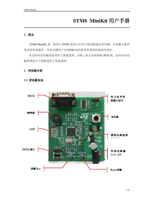
STM8 MiniKit 用户手册1.简介STM8 MiniKit 是一款基于STM8系列八位单片机的低成本评估板。
评估板上配有基本的外部器件,从而方便用户对STM8的内核及外设的性能进行评估。
本文档对评估板的使用作了简要说明,并附上相关原理图和PCB 图。
此外对评估板附带的5个例程也作了简要说明。
2.评估板介绍 2.1 评估板评估板布局布局2.2 原理图原理图与与PCB 原理图:PCB:3.参考代码说明随盘附赠的CD中共包含5个例程:Music:音乐播放例程;CSS:时钟切换及时钟安全系统的使用例程;Sinwave:正弦波发生例程;LED:LED控制例程;UART:串口与PC通讯例程;注:1)本例程仅适用于STM8S MiniKit评估板。
且调试时请确认模拟电源选择跳线已经连接到5V/3.3V。
2)所有的例程均使用Cosmic C语言编译器,用户请预先安装Cosmic C编译器。
3)所有项目均基于STVD 4.1.0集成开发环境,用户请预先安装相应软件。
4)所有例程使用STLink作为在线调试工具,请在进行在线调试前确认PC与STLink的硬件连接。
3.1 Music例程说明项目描述本例程通过采用pwm信号驱动蜂鸣器播放音乐并调节音量与音调,来说明如何使用Timer,ADC,GPIO,TLI:使用HSI为系统时钟源,并配置恰当的分频比;Timer2 CC1通道配置为PWM模式用以驱动蜂鸣器;Timer4 溢出中断用作LED1,LED2,LED3闪烁的时基;TLI(PD7)中断用来切换音乐的音调;ADC 采样电位器电压来调节占空比以控制音量。
项目文件main.c 包含"main" 函数的主程序stm8_interrupt_vector.c 中断向量表硬件环境将在线调试工具与目标板通过swim接口相连;在J1接口连接9~12v的直流电;使用电位器来调节蜂鸣器音量;使用按键可在高音调和低音调之间切换;如何开始可按照如下步骤调试:1)直接打开已经建立好的项目(..\Demo\Music\Demo.stw),或创建一个项目并且配置好所有的项目选项(可按默认值配置);2)编译这个项目Project->Rebuild all;3)下载程序到MCU进行调试:Debug->Start/Stop Debug Session4)运行程序:Debug->Run (F5)调节评估板上的电位器RV1来调节BUZZ音量;用按键来切换乐曲的音调;3个LED灯(LD1, LD2, LD3) 依次点亮。
一、如何用STLINK下载STM8如果想长期用串口下载,第一次下载就必须要用ST-LINK下载,由于考虑到部分同学没有ST-LINK,我们电子科技协会会先用ST-LINK将所有转接板下载一次,使用者可以直接用串口下载了,方便了广大同学。
不过在这里还是简单的介绍一下如何用ST-LINK下载。
第一步:打开STVP(ST Visual Programmer),图1所示图1然后按下File里的Open,打开你所想要下载的程序。
第二步:选择Configure -> Configure ST Visual Programmer。
然后会弹出一个窗口,如图2图2选择ST-LINK,SWIM,STM8S105X4.然后按确定回到原来的界面。
第三步:按下Program -> Current tab就可以把程序下载进去了。
注:硬件上就ST-LINK的SWIM接STM8的SWIM(PD1)脚,SWIM-RST接51板上的第9脚(NRST);还有VCC和GND就接开发板上的电源和地。
注意要供上电后才能下载。
二、如何用串口下载STM8注:要用Flash Loader Demonstrator2.2版本才能下载,下载前要把USB和串口下载的转换按键按下。
也就是中间那个按键按下,即选择了串口下载。
第一步:打开Flash Loader Demonstrator2.2 ,如图3设置,注意Echo要选择为Echo Mode。
然后按下STM8转接板上的复位按键,松手后马上点击Next。
图3第二步:连接成功后会弹出如图4警告,按确定就行了。
因为刚启动软件还没有选择合适器件,下载完毕不关掉软件再重复一次就没有这个警告了。
图4第三步:Target选择STM_32K,然后点Next。
图5第四步:这个界面可以选择擦除、下载、读取操作,我们主要目的是下载。
选择好下载文件,擦除(擦除必要页、不擦除、全部擦除)按需选择一项。
可以勾选的选项有:跳到用户程序(下载完毕)、优化(去掉某些0xFF)、下载后校检。

January 2023UM1075 Rev 91/19UM1075User manualST-LINK/V2 in-circuit debugger/programmerfor STM8 and STM32IntroductionThe ST-LINK/V2 is an in-circuit debugger/programmer for the STM8 and STM32microcontrollers. The single wire interface module (SWIM) and the JTAG/serial wire debugging (SWD) interfaces facilitate the communication with any STM8 or STM32 microcontroller operating on an application board.In addition to providing the same functionalities of the ST-LINK/V2, the ST-LINK/V2-ISOL features digital isolation between the PC and the target application board. It also withstands voltages of up to 1000 V RMS .The USB full-speed interface enables communication with a PC and:•STM8 devices via ST Visual Develop (STVD) or ST Visual Program (STVP) software (available from STMicroelectronics)•STM32 devices via IAR ™, Keil ®, STM32CubeIDE, STM32CubeProgrammer, and STM32CubeMonitor integrated development environments.Figure 1. ST-LINK/V2 and ST-LINK/V2-ISOLST-LINK/V2ST-LINK/V2-ISOLContents UM1075Contents1Features . . . . . . . . . . . . . . . . . . . . . . . . . . . . . . . . . . . . . . . . . . . . . . . . . . . 5 2Ordering information . . . . . . . . . . . . . . . . . . . . . . . . . . . . . . . . . . . . . . . . 5 3Product contents . . . . . . . . . . . . . . . . . . . . . . . . . . . . . . . . . . . . . . . . . . . . 64Hardware configuration . . . . . . . . . . . . . . . . . . . . . . . . . . . . . . . . . . . . . . 84.1Connection with STM8 . . . . . . . . . . . . . . . . . . . . . . . . . . . . . . . . . . . . . . . . 94.1.1Standard ERNI connection with SWIM flat ribbon . . . . . . . . . . . . . . . . . . 94.1.2Low-cost SWIM connection . . . . . . . . . . . . . . . . . . . . . . . . . . . . . . . . . . 104.1.3SWIM signals and connections . . . . . . . . . . . . . . . . . . . . . . . . . . . . . . . 104.2Connection with STM32 . . . . . . . . . . . . . . . . . . . . . . . . . . . . . . . . . . . . . . 124.3ST-LINK/V2 status LED . . . . . . . . . . . . . . . . . . . . . . . . . . . . . . . . . . . . . . 145Software configuration . . . . . . . . . . . . . . . . . . . . . . . . . . . . . . . . . . . . . . 155.1ST-LINK/V2 firmware upgrade . . . . . . . . . . . . . . . . . . . . . . . . . . . . . . . . . 155.2STM8 application development . . . . . . . . . . . . . . . . . . . . . . . . . . . . . . . . 155.3STM32 application development and flash programming . . . . . . . . . . . . 15 6Schematics . . . . . . . . . . . . . . . . . . . . . . . . . . . . . . . . . . . . . . . . . . . . . . . 16 7Revision history . . . . . . . . . . . . . . . . . . . . . . . . . . . . . . . . . . . . . . . . . . . 182/19UM1075 Rev 9UM1075List of tables List of tablesTable 1.List of the order codes . . . . . . . . . . . . . . . . . . . . . . . . . . . . . . . . . . . . . . . . . . . . . . . . . . . . . 5 Table 2.SWIM flat ribbon connections for ST-LINK/V2 . . . . . . . . . . . . . . . . . . . . . . . . . . . . . . . . . . 11 Table 3.SWIM low-cost cable connections for ST-LINK/V2-ISOL. . . . . . . . . . . . . . . . . . . . . . . . . . 11 Table 4.JTAG/SWD cable connections. . . . . . . . . . . . . . . . . . . . . . . . . . . . . . . . . . . . . . . . . . . . . . 12 Table 5.How third-party toolchains support ST-LINK/V2. . . . . . . . . . . . . . . . . . . . . . . . . . . . . . . . . 15 Table 6.Document revision history . . . . . . . . . . . . . . . . . . . . . . . . . . . . . . . . . . . . . . . . . . . . . . . . . 18UM1075 Rev 93/19List of figures UM1075 List of figuresFigure 1.ST-LINK/V2 and ST-LINK/V2-ISOL . . . . . . . . . . . . . . . . . . . . . . . . . . . . . . . . . . . . . . . . . . . 1 Figure 2.ST-LINK/V2 product contents. . . . . . . . . . . . . . . . . . . . . . . . . . . . . . . . . . . . . . . . . . . . . . . . 6 Figure 3.ST-LINK/V2-ISOL product contents . . . . . . . . . . . . . . . . . . . . . . . . . . . . . . . . . . . . . . . . . . . 7 Figure 4.ST-LINK/V2 (on the left) and ST-LINK/V2-ISOL (on the right) connectors. . . . . . . . . . . . . . 8 Figure 5.ERNI connector . . . . . . . . . . . . . . . . . . . . . . . . . . . . . . . . . . . . . . . . . . . . . . . . . . . . . . . . . . 9 Figure 6.Key detail on connectors . . . . . . . . . . . . . . . . . . . . . . . . . . . . . . . . . . . . . . . . . . . . . . . . . . 10 Figure 7.Low-cost connection. . . . . . . . . . . . . . . . . . . . . . . . . . . . . . . . . . . . . . . . . . . . . . . . . . . . . . 10 Figure 8.Target SWIM connector . . . . . . . . . . . . . . . . . . . . . . . . . . . . . . . . . . . . . . . . . . . . . . . . . . . 11 Figure 9.JTAG and SWD connection . . . . . . . . . . . . . . . . . . . . . . . . . . . . . . . . . . . . . . . . . . . . . . . . 13 Figure 10.JTAG debugging flat ribbon layout. . . . . . . . . . . . . . . . . . . . . . . . . . . . . . . . . . . . . . . . . . . 13 Figure 11.SWIM ST-LINK/V2 standard ERNI cable . . . . . . . . . . . . . . . . . . . . . . . . . . . . . . . . . . . . . . 16 Figure 12.SWIM ST-LINK/V2 low-cost cable . . . . . . . . . . . . . . . . . . . . . . . . . . . . . . . . . . . . . . . . . . . 17 4/19UM1075 Rev 9UM1075 Rev 95/19UM1075Features 1 Features•5 V power supplied by a USB connector •USB 2.0 full speed compatible interface •USB standard A to Mini-B cable •SWIM specific features–1.65 to 5.5 V application voltage supported on SWIM interface –SWIM low-speed and high-speed modes supported –SWIM programming-speed rate: 9.7 and 12.8 Kbytes/s, respectively, for low and high speed –SWIM cable for connection to the application via an ERNI standard vertical (ref: 284697 or 214017) or horizontal (ref: 214012) connector –SWIM cable for connection to the application via a pin header or a 2.54 mm pitch connector•JTAG/serial wire debugging (SWD) specific features – 1.65 to 3.6 V application voltage supported on the JTAG/SWD interface and 5 Vtolerant inputs (a)–JTAG cable for connection to a standard JTAG 20-pin pitch 2.54 mm connector–Supports JTAG communication, up to 9 MHz (default: 1.125 MHz)–Supports serial wire debug (SWD) up to 4 MHz (default: 1.8 MHz), and serial wireviewer (SWV) communication, up to 2 MHz •Direct firmware update feature supported (DFU)•Status LED, blinking during communication with the PC •1000 V RMS high isolation voltage (ST-LINK/V2-ISOL only)•Operating temperature from 0 to 50 °C2 Ordering informationTo order the ST-LINK/V2, refer to Table 1.a.The ST-LINK/V2 can communicate with targets operating below 3.3 V, but generates output signals at thisvoltage level. STM32 targets are tolerant to this over-voltage. If some other components of the target boardare sensible, use ST-LINK/V2-ISOL, STLINK-V3MINIE or STLINK-V3SET with B-STLINK-VOLT adapter toavoid impact of over-voltage injection on the board.Table 1. List of the order codesOrder codeST-LINK description ST-LINK/V2In-circuit debugger/programmer ST-LINK/V2-ISOL In-circuit debugger/programmer with digital isolationProduct contents UM10756/19UM1075 Rev 93 Product contentsThe cables delivered within the product are shown in Figure 2 and Figure 3. They include(from left to right):•USB standard A to Mini-B cable (A)•ST-LINK/V2 debugging and programming (B)•SWIM low-cost connector (C)•SWIM flat ribbon with a standard ERNI connector at one end (D) •JTAG or SWD and SWV flat ribbon with a 20-pin connector (E)Figure 2. ST-LINK/V2 product contentsABC D EUM1075Product contentsFigure 3. ST-LINK/V2-ISOL product contentsAB CDEUM1075 Rev 97/19Hardware configuration UM10758/19UM1075 Rev 94 Hardware configurationThe ST-LINK/V2 is designed around the STM32F103C8 device, which incorporates thehigh-performance Arm ®(a) Cortex ®-M3 core. It is available in a TQFP48 package.As shown in Figure 4, the ST-LINK/V2 provides two connectors:•an STM32 connector for the JTAG/SWD and SWV interface •an STM8 connector for the SWIM interfaceThe ST-LINK/V2-ISOL provides one connector for the STM8 SWIM, STM32 JTAG/SWD,and SWV interfaces.Figure 4. ST-LINK/V2 (on the left) and ST-LINK/V2-ISOL (on the right) connectors1. A = STM32 JTAG and SWD target connector2. B = STM8 SWIM target connector3. C = STM8 SWIM, STM32 JTAG, and SWD target connector4. D = Communication activity LEDa.Arm is a registered trademark of Arm Limited (or its subsidiaries) in the US and/or elsewhere.BA DCDUM1075 Rev 99/19UM1075Hardware configuration4.1 Connection with STM8For the development of applications based on STM8 microcontrollers, the ST-LINK/V2 canbe connected to the target board by two different cables, depending upon the connectoravailable on the application board.These cables are:•a SWIM flat ribbon with a standard ERNI connector at one end • a SWIM cable with two 4-pin, 2.54 mm connectors or SWIM separate-wires cables4.1.1 Standard ERNI connection with SWIM flat ribbonFigure 5 shows how to connect the ST-LINK/V2 if a standard ERNI 4-pin SWIM connector ispresent on the application board.Figure 5. ERNI connector1. A = Target application board with ERNI connector2. B = Wire cable with ERNI connector at one end3. C = STM8 SWIM target connector4.See Figure 11Figure 6 shows that pin 16 is missing on the ST-LINK/V2-ISOL target connector. Thismissing pin is used as a safety key on the cable connector, to guarantee the correct positionof the SWIM cable on the target connector even pins, used for both SWIM and JTAG cables.A BCABCHardware configuration UM107510/19UM1075 Rev 9Figure 6. Key detail on connectors 4.1.2 Low-cost SWIM connectionFigure 7 shows how to connect the ST-LINK/V2 if a 4-pin, 2.54 mm, low-cost SWIM connector is present on the application board.Figure 7. Low-cost connection1. A = Target application board with 4-pin,2.54 mm, low-cost connector2. B = Wire cable with a 4-pin connector or separate-wires cable3. C = STM8 SWIM target connector4.See Figure 124.1.3 SWIM signals and connectionsTable 2 summarizes the signal names, functions, and target connection signals when using the wire cable with a 4-pin connector.AB CA BCUM1075 Rev 911/19UM1075Hardware configurationFigure 8. Target SWIM connectorTable 3 summarizes the signal names, functions, and target connection signals using the separate-wires cable.As the SWIM separate-wires cable has independent connectors for all pins on one side, it is possible to connect the ST-LINK/V2-ISOL to an application board without a standard SWIM connector. On this flat ribbon, all signals are referenced by a specific color and a label to ease the connection on target.TVCC, SWIM, GND, and SWIM-RST can be connected to a low-cost 2.54 mm pitch connector or to pin headers available on the target board.Table 2. SWIM flat ribbon connections for ST-LINK/V2Pin Function Target connection1VDD Target VCC (1)1.The power supply from the application board is connected to the ST-LINK/V2 debugging and programmingboard to ensure signal compatibility between both boards.MCU VCC 2DATA SWIM MCU SWIM pin3GND GROUND GND 4RESETRESETMCU RESET pinTable 3. SWIM low-cost cable connections for ST-LINK/V2-ISOLColor Cable pin nameFunction Target connectionRed TVCC Target VCC (1)1.The power supply from the application board is connected to the ST-LINK/V2 debugging and programmingboard to ensure signal compatibility between both boards.MCU VCCGreen UART-RX Unused Reserved (2)(not connected on the target board)2.BOOT0, UART-TX and UART-RX are reserved for future developments.Blue UART-TX Yellow BOOT0Orange SWIM SWIM MCU SWIM pinBlack GND GROUND GND WhiteSWIM-RSTRESETMCU RESET pinHardware configuration UM107512/19UM1075 Rev 94.2 Connection with STM32For development of applications based on STM32 microcontrollers, the ST-LINK/V2 must be connected to the application using the standard 20-pin JTAG flat ribbon provided.Table 4 summarizes the signals names, functions, and target connection signals of the standard 20-pin JTAG flat ribbon.Table 4. JTAG/SWD cable connectionsPin no.ST-LINK/V2 connector (CN3)ST-LINK/V2function Target connection(JTAG)Target connection(SWD)1VAPP Target VCC MCU VDD (1)1.The power supply from the application board is connected to the ST-LINK/V2 debugging and programmingboard to ensure signal compatibility between the boards.MCU VDD (1)23TRST JTAG TRST JNTRST GND (2)2.Connect to GND for noise reduction on the ribbon.4GND (3)3.Available on ST-LINK/V2 only, not connected on ST-LINK/V2-ISOL.GND (3)GND (3)(4)4.At least one of these pin must be connected to the ground for correct behavior, it is recommended toconnecting all of them.GND (3)(4)5TDI JTAG TDO JTDI GND (2)6GND (3)GND (3)GND (3)(4)GND (3)(4)7TMS_SWDIO JTAG TMS, SW IO JTMS SWDIO 8GND (3)GND (3)GND (3)(4)GND (3)(4)9TCK_SWCLK JTAG TCK, SW CLK JTCK SWCLK 10GND (5)5.GND on ST-LINK/V2, used by SWIM on ST-LINK/V2-ISOL (see Table 3).GND (5)GND (4)(5)GND (4)(5)11Not connected Not connected Not connected Not connected 12GND GNDGND (4)GND (4)13TDO_SWO JTAG TDI, SWO JTDO TRACESWO (6)6.Optional: for Serial Wire Viewer (SWV) trace.14GND (5)GND (5)GND (4)(5)GND (4)(5)15NRST NRST NRST NRST 16GND (3)GND (3)GND (3)(4)GND (3)(4)17 Not connected Not connected Not connected Not connected 18GND GNDGND (4)GND (4)19VDD (3)VDD (3.3 V)(3)Not connected Not connected 20GNDGNDGND (4)GND (4)UM1075 Rev 913/19UM1075Hardware configurationFigure 9 shows how to connect the ST-LINK/V2 to a target using the JTAG cable.Figure 9. JTAG and SWD connection1. A = Target application board with JTAG connector2. B = JTAG/SWD 20-wire flat cable3. C = STM32 JTAG and SWD target connectorThe reference of the connector needed on the target application board is: 2x10C header wrapping 2x40C H3/9.5 (pitch 2.54) - HED20 SCOTT PHSD80.Note:For low cost applications, or when the standard 20-pin 2.54 mm-pitch connector footprint is too big, it is possible to implement the Tag-Connect solution. The Tag-Connect adapter and cable provide a simple and reliable means of connecting ST-LINK/V2 or ST-LINK/V2-ISOL to the PCB without requiring a mating component on the application PCB.ABCABCHardware configurationUM107514/19UM1075 Rev 9For more details on this solution and application-PCB-footprint information, visit .The references of components compatible with JTAG and SWD interfaces are:a) TC2050-ARM2010 adapter (20-pin- to 10-pin-interface board) b) TC2050-IDC or TC2050-IDC-NL (No Legs) (10-pin cable)c) TC2050-CLIP retaining clip for use with TC2050-IDC-NL (optional)4.3 ST-LINK/V2 status LEDThe LED labeled COM on top of the ST-LINK/V2 shows the ST-LINK/V2 status (whatever the connection type). In detail:•LED is blinking RED: the first USB enumeration with the PC is taking place•LED is RED: communication between the PC and ST-LINK/V2 is established (end of enumeration)•LED is blinking GREEN / RED: data are exchanged between the target and the PC •LED is GREEN: the last communication has been successful•LED is ORANGE: ST-LINK/V2 communication with the target has failed.UM1075 Rev 915/19UM1075Software configuration5 Software configuration5.1 ST-LINK/V2 firmware upgradeThe ST-LINK/V2 embeds a firmware upgrade mechanism for in-situ upgrade through theUSB port. As the firmware can evolve during the life of the ST-LINK/V2 product (new functionality, bug fixes, support for new microcontroller families), it is recommended to periodically visit the dedicated pages on to stay up-to-date with the latest version.5.2 STM8 application developmentRefer to ST toolset Pack24 with Patch 1 or more recent, which includes ST Visual Develop (STVD) and ST Visual Programmer (STVP).5.3 STM32 application development and flash programmingThird-party toolchains (IAR ™ EWARM, Keil ® MDK-ARM ™) support ST-LINK/V2 according to the versions given in Table 5 or in the most recent version available.The ST-LINK/V2 requires a dedicated USB driver. If the toolset setup does not install it automatically, the driver can be found on under the name STSW-LINK009.For more information on third-party tools, visit the following websites:• •Table 5. How third-party toolchains support ST-LINK/V2Third party Toolchain Version IAR ™EWARM 6.20Keil ®MDK-ARM ™4.20Schematics UM107516/19UM1075 Rev 96 Schematics1.Legend for pin descriptions:VDD = Target voltage senseDATA = SWIM DATA line between target and debug tool GND = Ground voltageRESET = Target system resetUM1075Schematics1.Legend for pin descriptions:VDD = Target voltage senseDATA = SWIM DATA line between target and debug toolGND = Ground voltageRESET = Target system resetUM1075 Rev 917/19Revision history UM107518/19UM1075 Rev 97 Revision historyTable 6. Document revision historyDate RevisionChanges22-Apr-20111Initial release.03-Jun-20112Table 2: SWIM flat ribbon connections for ST-LINK/V2: addedfootnote 1 to the function “Target VCC”.Table 4: JTAG/SWD cable connections : added footnote to the function “Target VCC”.Table 5: How third-party toolchains support ST-LINK/V2: updated the “Versions” of IAR and Keil.19-Aug-20113Added USB driver details to Section 5.3.11-May-20124Added SWD and SWV to JTAG connection features. Modified Table 4: JTAG/SWD cable connections .13-Sep-20125Added ST-LINK/V2-ISOL order code.Updated Section 4.1: STM8 application development on page 15.Added Note 6 in Table 4.Added Note “For low cost applications...” before Section 3.3: ST-LINK/V2 status LEDs on page 14.18-Oct-20126Added Section 5.1: ST-LINK/V2 firmware upgrade on page 15.25-Mar-20167Updated V RMS value in Introduction and in Features .18-Oct-20188Updated Table 4: JTAG/SWD cable connections and its footnotes.Minor text edits across the whole document.09-Jan-20239Updated Introduction , Features , and Section 5.3: STM32 application development and flash programming .Updated Table 5: How third-party toolchains support ST-LINK/V2.Minor text edits across the whole document.UM1075IMPORTANT NOTICE – READ CAREFULLYSTMicroelectronics NV and its subsidiaries (“ST”) reserve the right to make changes, corrections, enhancements, modifications, and improvements to ST products and/or to this document at any time without notice. Purchasers should obtain the latest relevant information on ST products before placing orders. ST products are sold pursuant to ST’s terms and conditions of sale in place at the time of order acknowledgment.Purchasers are solely responsible for the choice, selection, and use of ST products and ST assumes no liability for application assistance or the design of purchasers’ products.No license, express or implied, to any intellectual property right is granted by ST herein.Resale of ST products with provisions different from the information set forth herein shall void any warranty granted by ST for such product. ST and the ST logo are trademarks of ST. For additional information about ST trademarks, refer to /trademarks. All other product or service names are the property of their respective owners.Information in this document supersedes and replaces information previously supplied in any prior versions of this document.© 2023 STMicroelectronics – All rights reservedUM1075 Rev 919/19。
数据手册STM8S105xx 基础型系列,16MHz STM8S 8位单片机,多达32K字节Flash 集成数据EEPROM,10位ADC,定时器,UART,SPI,I²C芯片特点内核高级STM8内核,具有3级流水线的哈佛结构扩展指令集存储器中等密度程序和数据存储器:─最多32K字节Flash;10K次擦写后在55°C环境下数据可保存20年─数据存储器:多达1K字节真正的数据EEPROM;可达30万次擦写RAM:多达2K字节时钟、复位和电源管理2.95 ~ 5.5V工作电压灵活的时钟控制,4个主时钟源– 低功率晶体振荡器– 外部时钟输入– 用户可调整的内部16MHz RC– 内部低功耗128kHz RC带有时钟监控的时钟安全保障系统电源管理:– 低功耗模式(等待、活跃停机、停机) – 外设的时钟可单独关闭永远打开的低功耗上电和掉电复位中断管理带有32个中断的嵌套中断控制器6个外部中断向量,最多37个外部中断定时器2个16位通用定时器,带有2+3个CAPCOM通道(IC、OC 或 PWM)高级控制定时器:16位,4个CAPCOM 通道,3个互补输出,死区插入和灵活的同步带有8位预分频器的8位基本定时器自动唤醒定时器2个看门狗定时器:窗口看门狗和独立看门狗通信接口带有同步时钟输出的UART ,智能卡,红外IrDA,LIN接口SPI接口最高到8Mbit/sI2C接口最高到400Kbit/s模数转换器(ADC)10位,±1LSB的ADC,最多有10路通道,扫描模式和模拟看门狗功能I/O端口48脚封装芯片上最多有38个I/O,包括16个高吸收电流输出非常强健的I/O设计,对倒灌电流有非常强的承受能力开发支持单线接口模块(SWIM)和调试模块(DM),可以方便地进行在线编程和非侵入式调试表1产品列表系列型号STM8S105xxSTM8S105K4, STM8S105K6,STM8S105S4, STM8S105S6,STM8S105C4, STM8S105C6本文档英文原文下载地址:/stonline/products/literature/ds/14771.pdf目录1简介 (4)2详细描述 (5)3模块框图 (6)4产品概述 (7)4.1STM8的中央处理单元 (7)4.2单线接口模块(SWIM)和调试模块(DM) (7)4.3中断控制器 (8)4.4Flash程序存储器和数据EEPROM存储器 (8)4.5时钟控制器 (9)4.6电源管理 (9)4.7看门狗定时器 (10)4.8自动唤醒计数器 (10)4.9蜂鸣器 (10)4.10TIM1 — 16位高级控制定时器 (10)4.11TIM2、TIM3 — 16位通用定时器 (10)4.12TIM4 — 8位基本定时器 (11)4.13模数转换器(ADC1) (11)4.14通信接口 (11)4.14.1UART2 (11)4.14.2SPI (12)4.14.3I2C (12)5引脚及其描述 (13)5.1封装引脚 (13)5.1.1备选功能重映射 (19)6存储器和寄存器映像 (20)6.1存储器映像 (20)6.2寄存器映像 (21)7中断向量映像 (28)8选项字节 (29)9电气特性 (32)9.1参数条件 (32)9.1.1最小和最大值 (32)9.1.2典型数值 (32)9.1.3典型曲线 (32)9.1.4典型电流消耗 (32)9.1.5引脚的负载条件 (32)9.1.6负载电容 (32)9.1.7引脚输入电压 (33)9.2绝对最大额定值 (33)9.3工作条件 (34)9.3.1VCAP外部电容 (35)9.3.2供电电流特性 (35)9.3.3外部时钟源和时间特性 (41)9.3.4内部时钟源和时间特性 (43)9.3.5存储器特性 (44)9.3.6I/O端口管脚特性 (45)9.3.7复位管脚特性 (50)9.3.8串行外设接口(SPI) (52)9.3.9I2C接口特性 (54)9.3.1010位ADC特性 (55)9.3.11EMC特性 (57)10封装特性 (60)10.1封装机械数据 (60)10.1.1LQFP封装尺寸 (60)10.1.2VFQFPN封装机械数据 (63)10.1.3SDIP32封装机械数据 (64)10.2热特性 (64)10.2.1参考文档 (65)10.2.2选择产品的温度范围 (65)11订购信息 (66)12STM8开发工具 (本章从略) (67)12.1仿真和在线调试工具 (67)12.2软件工具 (67)12.2.1STM8工具套件 (67)12.2.2C和汇编工具 (67)12.3编程工具 (67)13(英文)版本修改记录 (68)1 简介这本数据手册描述了STM8S105xx基础型系列单片机的特点、引脚分配、电气特性、机械特性和订购信息。
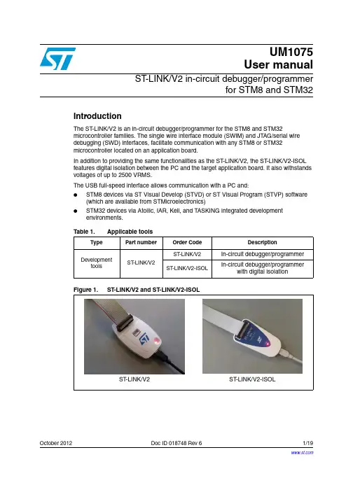
October 2012Doc ID 018748 Rev 61/19UM1075User manualST -LINK/V2 in-circuit debugger/programmerfor STM8 and STM32IntroductionThe ST -LINK/V2 is an in-circuit debugger/programmer for the STM8 and STM32microcontroller families. The single wire interface module (SWIM) and JTAG/serial wire debugging (SWD) interfaces, facilitate communication with any STM8 or STM32 microcontroller located on an application board.In addition to providing the same functionalities as the ST -LINK/V2, the ST -LINK/V2-ISOL features digital isolation between the PC and the target application board. It also withstands voltages of up to 2500 VRMS.The USB full-speed interface allows communication with a PC and:●STM8 devices via ST Visual Develop (STVD) or ST Visual Program (STVP) software (which are available from STMicroelectronics)●STM32 devices via Atollic, IAR, Keil, and TASKING integrated development environments.Figure 1.ST-LINK/V2 and ST -LINK/V2-ISOLTable 1.Applicable toolsTypePart numberOrder Code DescriptionDevelopmenttoolsST -LINK/V2ST -LINK/V2In-circuit debugger/programmer ST -LINK/V2-ISOLIn-circuit debugger/programmerwith digital isolationST -LINK/V2ST -LINK/V2-ISOLContents UM1075Contents1Features . . . . . . . . . . . . . . . . . . . . . . . . . . . . . . . . . . . . . . . . . . . . . . . . . . . 5 2Product contents . . . . . . . . . . . . . . . . . . . . . . . . . . . . . . . . . . . . . . . . . . . . 63Hardware configuration . . . . . . . . . . . . . . . . . . . . . . . . . . . . . . . . . . . . . . 83.1Connection with STM8 applications . . . . . . . . . . . . . . . . . . . . . . . . . . . . . . 83.1.1Standard ERNI connection with SWIM flat ribbon . . . . . . . . . . . . . . . . . . 93.1.2Low-cost SWIM connection . . . . . . . . . . . . . . . . . . . . . . . . . . . . . . . . . . 103.1.3SWIM signals and connections . . . . . . . . . . . . . . . . . . . . . . . . . . . . . . . 113.2Connection with STM32 applications . . . . . . . . . . . . . . . . . . . . . . . . . . . . 123.3ST-LINK/V2 status LEDs . . . . . . . . . . . . . . . . . . . . . . . . . . . . . . . . . . . . . 144Software configuration . . . . . . . . . . . . . . . . . . . . . . . . . . . . . . . . . . . . . . 154.1ST-Link/V2 firmware upgrade . . . . . . . . . . . . . . . . . . . . . . . . . . . . . . . . . . 154.2STM8 application development . . . . . . . . . . . . . . . . . . . . . . . . . . . . . . . . 154.3STM32 application development and Flash programming . . . . . . . . . . . . 15 5Schematics . . . . . . . . . . . . . . . . . . . . . . . . . . . . . . . . . . . . . . . . . . . . . . . 16 6Revision history . . . . . . . . . . . . . . . . . . . . . . . . . . . . . . . . . . . . . . . . . . . 182/19Doc ID 018748 Rev 6UM1075List of tables List of tablesTable 1.Applicable tools. . . . . . . . . . . . . . . . . . . . . . . . . . . . . . . . . . . . . . . . . . . . . . . . . . . . . . . . . . . 1 Table 2.SWIM flat ribbon connections for ST-LINK/V2 . . . . . . . . . . . . . . . . . . . . . . . . . . . . . . . . . . 11 Table 3.SWIM low-cost cable connections for ST-LINK/V2-ISOL. . . . . . . . . . . . . . . . . . . . . . . . . . 11 Table 4.JTAG/SWD cable connections. . . . . . . . . . . . . . . . . . . . . . . . . . . . . . . . . . . . . . . . . . . . . . 12 Table 5.How third party toolchains support ST-LINK/V2. . . . . . . . . . . . . . . . . . . . . . . . . . . . . . . . . 15 Table 6.Document revision history . . . . . . . . . . . . . . . . . . . . . . . . . . . . . . . . . . . . . . . . . . . . . . . . . 18Doc ID 018748 Rev 63/19List of figures UM1075 List of figuresFigure 1.ST-LINK/V2 and ST-LINK/V2-ISOL . . . . . . . . . . . . . . . . . . . . . . . . . . . . . . . . . . . . . . . . . . . 1 Figure 2.ST-LINK/V2 product contents. . . . . . . . . . . . . . . . . . . . . . . . . . . . . . . . . . . . . . . . . . . . . . . . 6 Figure 3.ST-LINK/V2-ISOL product contents . . . . . . . . . . . . . . . . . . . . . . . . . . . . . . . . . . . . . . . . . . . 7 Figure 4.Connectors of the ST-LINK/V2 and ST-LINK/V2-ISOL. . . . . . . . . . . . . . . . . . . . . . . . . . . . . 8 Figure 5.ERNI connection. . . . . . . . . . . . . . . . . . . . . . . . . . . . . . . . . . . . . . . . . . . . . . . . . . . . . . . . . . 9 Figure 6.Key detail on connectors . . . . . . . . . . . . . . . . . . . . . . . . . . . . . . . . . . . . . . . . . . . . . . . . . . . 9 Figure 7.Low-cost connection. . . . . . . . . . . . . . . . . . . . . . . . . . . . . . . . . . . . . . . . . . . . . . . . . . . . . . 10 Figure 8.Target SWIM connector . . . . . . . . . . . . . . . . . . . . . . . . . . . . . . . . . . . . . . . . . . . . . . . . . . . 11 Figure 9.JTAG and SWD connection . . . . . . . . . . . . . . . . . . . . . . . . . . . . . . . . . . . . . . . . . . . . . . . . 13 Figure 10.JTAG debugging flat ribbon layout. . . . . . . . . . . . . . . . . . . . . . . . . . . . . . . . . . . . . . . . . . . 13 Figure 11.SWIM ST-LINK/V2 standard ERNI cable . . . . . . . . . . . . . . . . . . . . . . . . . . . . . . . . . . . . . . 16 Figure 12.SWIM ST-LINK/V2 low-cost cable . . . . . . . . . . . . . . . . . . . . . . . . . . . . . . . . . . . . . . . . . . . 17 4/19Doc ID 018748 Rev 6UM1075Features1 Features● 5 V power supplied by a USB connector●USB 2.0 full speed compatible interface●USB standard A to mini B cable●SWIM specific features– 1.65 V to 5.5 V application voltage supported on SWIM interface–SWIM low-speed and high-speed modes supported–SWIM programming speed rate: 9.7 Kbytes/s in low speed and 12.8 Kbytes/s in high speed–SWIM cable for connection to the application via an ERNI standard vertical(ref: 284697 or 214017) or horizontal (ref: 214012) connector–SWIM cable for connection to the application via a pin header or a 2.54 mm pitch connector●JTAG/serial wire debugging (SWD) specific features– 1.65 V to 3.6 V application voltage supported on the JT AG/SWD interface and 5 V tolerant inputs–JTAG cable for connection to a standard JTAG 20-pin pitch 2.54 mm connector–Supports JTAG communication–Supports serial wire debug (SWD) and serial wire viewer (SWV) communication●Direct firmware update feature supported (DFU)●Status LED which blinks during communication with the PC●2500 VRMS high isolation voltage (ST-LINK/V2-ISOL only)●Operating temperature 0 to 50 °CDoc ID 018748 Rev 65/19Product contents UM10756/19Doc ID 018748 Rev 62 Product contentsFigures ST -LINK/V2 product contents show the various cables delivered within the product.They include (from left to right in Figure 2 and Figure 3):●USB standard A to mini B cable (A)●ST -LINK/V2 debugging and programming (B)●SWIM low-cost connector (C)●SWIM flat ribbon with a standard ERNI connector at one end (D) ●JTAG or SWD and SWV flat ribbon with a 20-pin connector (E)Figure 2.ST-LINK/V2 product contentsABCDEUM1075Product contentsDoc ID 018748 Rev 67/19Figure 3.ST-LINK/V2-ISOL product contentsABCDEHardware configuration UM10758/19Doc ID 018748 Rev 63 Hardware configurationThe ST -LINK/V2 is designed around the STM32F103C8 device which incorporates the high-performance ARM®, Cortex™-M3 core. It is available in a TQFP48 package. As shown in Figure 4, the ST -LINK/V2 provides two connectors:●an STM32 connector for the JTAG/SWD and SWV interface ●an STM8 connector for the SWIM interfaceThe ST -LINK/V2-ISOL provides one connector for the STM8 SWIM, STM32 JTAG/SWD andSWV interfaces.Figure 4.Connectors of the ST-LINK/V2 and ST-LINK/V2-ISOL1. A = STM32 JTAG and SWD target connector2. B = STM8 SWIM target connector3. C = STM8 SWIM, STM32 JTAG and SWD target connector4. D = Communication activity LED3.1 Connection with STM8 applicationsFor STM8 developments, the ST -LINK/V2 can be connected to the target board by two different cables, depending on the connector available on the application board. These cables are:●SWIM flat ribbon with a standard ERNI connector at one end●SWIM cable with two 4-pin, 2.54 mm connector or SWIM separate-wires cableBA DCDUM1075Hardware configurationDoc ID 018748 Rev 69/193.1.1 Standard ERNI connection with SWIM flat ribbonFigure 5 shows how to connect the ST -LINK/V2 if a standard ERNI 4-pin SWIM connector is present on the application board. Figure 5.ERNI connection1.A = Target application board with ERNI connector 2.B = Wire cable with ERNI connector at one end3. C = STM8 SWIM target connector4.See Figure 11: SWIM ST-LINK/V2 standard ERNI cable .Figure 6 shows that pin 16 is missing on the ST -LINK/V2-ISOL target connector. Thismissing pin is used as a safety key on the cable connector to guarantee connection of the SWIM cable in the correct position on the target connector even pins, used for both SWIM and JTAG cables.Figure 6.Key detail on connectorsABCABCHardware configuration UM107510/19Doc ID 018748 Rev 63.1.2 Low-cost SWIM connectionFigure 7 shows how to connect the ST -LINK/V2 if a 4-pin, 2.54 mm, low-cost SWIMconnector is present on the application board.Figure 7.Low-cost connection1. A = Target application board with 4-pin,2.54 mm, low-cost connector 2. B = Wire cable with a 4-pin connector or separate-wires cable3. C = STM8 SWIM target connector4.See Figure 12: SWIM ST-LINK/V2 low-cost cableA BCABCUM1075Hardware configurationDoc ID 018748 Rev 611/193.1.3 SWIM signals and connectionsTable 2 summarizes the signal names, functions, and target connection signals using thewire cable with a 4-pin connector.Figure 8.Target SWIM connectorTable 3 summarizes the signal names, functions, and target connection signals using the separate-wires cable.As the SWIM separate-wires cable has independent connectors for all pins on one side, it is possible to connect the ST -LINK/V2-ISOL to an application board without a standard SWIM connector. On this flat ribbon, all signals are referenced by a specific color and a label to ease the connection on target.Table 2.SWIM flat ribbon connections for ST-LINK/V2Pin Function Target connection1VDD TargetVCC (1)1.The power supply from the application board is connected to the ST-LINK/V2 debugging and programmingboard to ensure signal compatibility between both boards.MCU VCC 2DA TA SWIM MCU SWIM pin3GND GROUND GND 4RESETRESETMCU RESET pinTable 3.SWIM low-cost cable connections for ST-LINK/V2-ISOLColor Cable pin nameFunction Target connectionRed TVCC Target VCC (1)1.The power supply from the application board is connected to the ST-LINK/V2 debugging and programmingboard to ensure signal compatibility between both boards.MCU VCCGreen UART -RX Unused Reserved (2)(not connected on the target board)2.BOOT0, UART-TX and UART-RX are reserved for future developments.Blue UART -TX Y ellow BOOT0Orange SWIM SWIM MCU SWIM pinBlack GND GROUND GND WhiteSWIM-RSTRESETMCU RESET pinHardware configuration UM107512/19Doc ID 018748 Rev 6TVCC, SWIM, GND and SWIM-RST can be connected to a low-cost 2.54 mm pitch connector or to pin headers available on the target board.3.2 Connection with STM32 applicationsFor STM32 developments, the ST -LINK/V2 needs to be connected to the application using the standard 20-pin JT AG flat ribbon provided.Table 4 summarizes the signals names, functions, and target connection signals of the standard 20-pin JTAG flat ribbon.Table 4.JTAG/SWD cable connectionsPin no.ST-LINK/V2 connector (CN3)ST-LINK/V2 functionTarget connection(JTAG)Target connection(SWD)1VAPP T arget VCC MCU VDD (1)1.The power supply from the application board is connected to the ST-LINK/V2 debugging and programmingboard to ensure signal compatibility between both boards.MCU VDD (1)23TRST JTAG TRST JNTRST GND (2)2.Connect to GND for noise reduction on the ribbon.4GNDGNDGND (3)3.At least one of this pin must be connected to the ground for correct behavior (connecting all of them isrecommended).GND (3)5TDI J TAG TDO J TDI GND (2)6GND GNDGND (3)GND (3)7TMS_SWDIO JTAG TMS, SW IO JTMS SWDIO 8GND GNDGND (3)GND (3)9TCK_SWCLK JTAG TCK, SW CLK JTCK SWCLK 10GND GNDGND (3)GND (3)11NCNot connectedNot connected Not connected 12GND GND GND (3)GND (3)13TDO_SWO JTAG TDI, SWO JTDO TRACESWO (4)4.Optional: for Serial Wire Viewer (SWV) trace.14GND GND GND (3)GND (3)15NRSTNRSTNRSTNRST16GND GND GND (3) GND (3)17 NC Not connected Not connected Not connected 18GND GND GND (3)GND (3)19VDD VDD (3.3V)(5)5.Available on ST-LINK/V2 only and not connected on ST-LINK/V2/OPTO.Not connectedNot connected 20GNDGND GND (3)GND (3)UM1075Hardware configurationDoc ID 018748 Rev 613/19Figure 9 shows how to connect the ST -LINK/V2 to a target using the JTAG cable.Figure 9.JTAG and SWD connection1. A = Target application board with JTAG connector2. B = JTAG/SWD 20-wire flat cable3.C= STM32 JTAG and SWD target connectorThe reference of the connector needed on the target application board is:2x10C header wrapping 2x40C H3/9.5 (pitch 2.54) - HED20 SCOTT PHSD80.Note:For low cost applications or when the standard 20 pins pitch 2.54mm connector footprint is too big, it is possible to implement the Tag-Connect solution to save cost and space on the application board. The Tag-Connect adapter and cable provide a simple reliable means of connecting ST -LINK/V2 or ST -LINK/V2-ISOL to your PCB without requiring a matingABCABCHardware configuration UM107514/19Doc ID 018748 Rev 6component on application PCB. For more details on this solution and application PCB footprint information, please visit .The references of components compatible with JTAG and SWD interfaces are:a) TC2050-ARM2010 adapter (20pins to 10pins interface board) b) TC2050-IDC or TC2050-IDC-NL (No Legs) (10pins cable)c)TC2050-CLIP retaining clip for use with TC2050-IDC-NL (optional)3.3 ST-L INK/V2 status LEDsThe LED labeled ‘COM’ on top of the ST -LINK/V2 shows the ST -LINK/V2 status (whateverthe connection type). When the:●LED is blinking RED: the first USB enumeration with the PC is taking place.●LED is RED: communication between the PC and ST -LINK/V2 is established (end of enumeration).●LED is blinking GREEN/RED: data are being exchanged between the target and the PC.●LED is GREEN: the last communication has been successful.●LED is ORANGE: ST -LINK/V2 communication with the target has failed.UM1075Software configurationDoc ID 018748 Rev 615/194 Software configuration4.1ST-Link/V2 firmware upgradeThe ST -Link/V2 embeds a firmware upgrade mechanism for in-situ upgrade through theUSB port. As the firmware might evolve during the whole life of the ST -Link/V2 product (new functionality, bug fixes, support for new microcontroller families …), it is recommended to visit /stlinkv2 periodically in order to stay up-to-date with the latest firmware version.4.2 STM8 application developmentPlease refer to ST toolset Pack24 with Patch 1 or more recent, which includes ST Visual Develop (STVD) and ST Visual Programmer (STVP).4.3 STM32 application development and Flash programmingThird party toolchains, Atollic TrueSTUDIO, IAR EWARM, Keil MDK-ARM, and TASKING VX-toolset support ST -LINK/V2 according to the versions given in Table 5 or the most recent version available.The ST -LINK/V2 requires a dedicated USB driver. If the toolset installed it automatically, file stlink_winusb.inf is installed in <WINDIR>/inf (where <WINDIR> is typically C:/Windows). If the toolset setup did not install it automatically, the driver can be found on :1.Connect to .2. In the search tab, part number field, look for ST-Link/V2.3.Click on the Generic Part Number column’s hyperlink to ST -Link/V2.4. In the Design support tab, SW drivers section, click on the icon to download st-link_v2_usbdriver.zip.5.Unzip and run ST -Link_V2_USBdriver.exe.For more information on third party tools, please visit:● ● ● ●Table 5.How third party toolchains support ST -LINK/V2Third partyToolchainVersionAtollic TrueSTUDIO 2.1IAR EWARM 6.20Keil MDK-ARM 4.20T ASKINGVX-toolset for ARM Cortex-M4.0.1Schematics UM107516/19Doc ID 018748 Rev 65 Schematics1.Legend for pin descriptions:VDD = Target voltage senseDATA = SWIM DATA line between target and debug tool GND = Ground voltageRESET = Target system resetUM1075SchematicsDoc ID 018748 Rev 617/191.Legend for pin descriptions:VDD = Target voltage senseDATA = SWIM DATA line between target and debug tool GND = Ground voltageRESET = Target system resetRevision history UM107518/19Doc ID 018748 Rev 66 Revision historyTable 6.Document revision historyDate RevisionChanges22-Apr-20111Initial release.03-Jun-20112Table 2: SWIM flat ribbon connections for ST -LINK/V2: addedfootnote 1 to the function “Target VCC”.Table 4: JT AG/SWD cable connections : added footnote to the function “Target VCC”.Table 5: How third party toolchains support ST -LINK/V2: updated the “Versions” of IAR and Keil.19-Aug-20113Added USB driver details to Section 4.3.11-May-20124Added SWD and SWV to JT AG connection features. Modified Table 4: JT AG/SWD cable connections .13-Sep-20125Added ST -LINK/V2-ISOL order code.Updated Section 4.1: STM8 application development on page 15Added Note 5. in T able 4.Added Note “For low cost applications...” before Section 3.3: ST -LINK/V2 status LEDs on page 1418-Oct-20126Added Section 4.1: ST -Link/V2 firmware upgrade on page 15.UM1075Please Read Carefully:Information in this document is provided solely in connection with ST products. STMicroelectronics NV and its subsidiaries (“ST”) reserve the right to make changes, corrections, modifications or improvements, to this document, and the products and services described herein at any time, without notice.All ST products are sold pursuant to ST’s terms and conditions of sale.Purchasers are solely responsible for the choice, selection and use of the ST products and services described herein, and ST assumes no liability whatsoever relating to the choice, selection or use of the ST products and services described herein.No license, express or implied, by estoppel or otherwise, to any intellectual property rights is granted under this document. If any part of this document refers to any third party products or services it shall not be deemed a license grant by ST for the use of such third party products or services, or any intellectual property contained therein or considered as a warranty covering the use in any manner whatsoever of such third party products or services or any intellectual property contained therein.UNL ESS OTHERWISE SET FORTH IN ST’S TERMS AND CONDITIONS OF SAL E ST DISCL AIMS ANY EXPRESS OR IMPL IED WARRANTY WITH RESPECT TO THE USE AND/OR SAL E OF ST PRODUCTS INCL UDING WITHOUT L IMITATION IMPL IED WARRANTIES OF MERCHANTABILITY, FITNESS FOR A PARTICULAR PURPOSE (AND THEIR EQUIVALENTS UNDER THE LAWS OF ANY JURISDICTION), OR INFRINGEMENT OF ANY PATENT, COPYRIGHT OR OTHER INTELLECTUAL PROPERTY RIGHT. UNL ESS EXPRESSL Y APPROVED IN WRITING BY TWO AUTHORIZED ST REPRESENTATIVES, ST PRODUCTS ARE NOT RECOMMENDED, AUTHORIZED OR WARRANTED FOR USE IN MILITARY, AIR CRAFT, SPACE, LIFE SAVING, OR LIFE SUSTAINING APPLICATIONS, NOR IN PRODUCTS OR SYSTEMS WHERE FAILURE OR MALFUNCTION MAY RESULT IN PERSONAL INJURY, DEATH, OR SEVERE PROPERTY OR ENVIRONMENTAL DAMAGE. ST PRODUCTS WHICH ARE NOT SPECIFIED AS "AUTOMOTIVE GRADE" MAY ONLY BE USED IN AUTOMOTIVE APPLICATIONS AT USER’S OWN RISK.Resale of ST products with provisions different from the statements and/or technical features set forth in this document shall immediately void any warranty granted by ST for the ST product or service described herein and shall not create or extend in any manner whatsoever, any liability of ST.ST and the ST logo are trademarks or registered trademarks of ST in various countries.Information in this document supersedes and replaces all information previously supplied.The ST logo is a registered trademark of STMicroelectronics. All other names are the property of their respective owners.© 2012 STMicroelectronics - All rights reservedSTMicroelectronics group of companiesAustralia - Belgium - Brazil - Canada - China - Czech Republic - Finland - France - Germany - Hong Kong - India - Israel - Italy - Japan - Malaysia - Malta - Morocco - Philippines - Singapore - Spain - Sweden - Switzerland - United Kingdom - United States of AmericaDoc ID 018748 Rev 619/19。
STM8L中文参考手册(4)-20 16位通用定时器(TIM2、TIM3、tim5)20.1简介本章介绍TIM2、TIM3和tim5是相同的定时器每个定时器包括一个由可编程分频器驱动的16位上下自动重载计数器它可以用于多种目的,包括:●定时产生●测量输入信号的脉冲长度(输入捕获)●产生输出波形(输出比较、脉宽调制和脉冲模式)●各种中断能力事件(捕获、比较、溢出)●与其他定时器或外部信号(外部时钟、复位、触发使能)同步定时器时钟可以来自内部时钟,也可以来自配置寄存器或外部源本章仅介绍通用定时器的主要特性。
它参考了与19:16高级控制定时器(TIM1)相对应的部分中的每个功能的更详细的信息页28320.2 TIMx 主要功能通用TIMx TIM2/TIM3功能包括:●16位向上、向下、向上/向下自动刷新计数器●3位可编程分频器允许将计数器的时钟频率分成1至128的任意2次方两个独立的低电平通道:输入捕获输出比较脉冲宽度调制产生(边沿对齐)-一个脉冲输出模式低电平中断输入,用于复位定时器输出信号,或处于已知状态●输入捕捉2可通过来自comp2比较器:更新的中断和DMA请求产生以下事件:当计数器溢出时,计数器初始化(软件)输入捕捉输出比较中断输入触发事件(开始、停止、内部/外部触发初始化或计数)20.3.1时间单元定时器时基单元包括:●16位可逆计数器时钟源是内部时钟(fsysclk)它由预分频器计数器的时钟ck_cnt驱动,预分频器计数器直接连接到ck_psc时钟馈送分频器分频器的实现如下:7位计数器(在timx_pscr寄存器中)由基于低预分频器的3位寄存器控制它可以控制飞行中寄存器缓冲区的变化。
它可以将计数器的时钟频率转换为1、2、4、8、16、32、64或128计数器的时钟频率计算如下:fCk _ CNT = fck _ PSC/2(PSCR[2:0)计数器操作请参考第19.3.4页:上部288,模式部分19.3.5:在第290页向下计数,模式19.3.6:中心对齐(向上/向下计数)29220.3.2时钟/触发控制器参见第296页第19.4节:TIM1时钟/触发控制器20.3.3采集/比较通道输入级参见第310页第19.5节:TIM1采集/比较通道有两个输入通道,如图122:输入级框图通道2内部连接到比较器输出级参见第19.5.4页:315,输出级19.5.5:强制输出模式在第316页,第19.5.7页:脉宽调制模式在第318页如图124所示。
STM8L中文参考手册-420个16位通用定时器(TIM2,TIM3,tim5)20.1引言本章介绍TIM2,TIM3和tim5是相同的定时器。
每个定时器包括一个16位的升降自动重载计数器由一个可编程分频器驱动。
它可用于多种用途,包括:●时基产生●测量输入信号的脉冲长度(输入捕捉)●生成输出波形(输出比较,脉宽调制和脉冲模式)●中断能力的各种事件(捕获,比较,溢出)●同步与其他计时器或外部信号(外部时钟,复位,触发使)定时器时钟可以来自内部时钟可以通过配置寄存器或从外部源。
只有通用定时器的主要特点是本章中提出的。
指的是部分19:16点先进控制定时器对应的段落(TIM1)对每个功能的更多详细信息页面283。
20.2 TIMx主要特点通用TIMx TIM2 / TIM3功能包括:●16位上,下,上/ downauto刷新计数器。
●3位可编程分频器使计数器的时钟频率可分‖ 飞‖的任何权力,2从1到128。
2个独立的通道●:输入捕捉输出比较PWM生成(边缘对齐方式)-一个脉冲输出的方式●中断输入将定时器的输出信号在复位状态,或在一个已知状态。
●输入捕捉2可以通过从comp2比较器●中断和DMA请求生成下列事件:更新:计数器溢出时,计数器初始化(软件)输入捕捉输出比较中断输入触发事件(计数器的启动,停止,内部/外部触发初始化或计数)20.3.1时间单位计时器时基单元包括:●16位可逆计数器●16位自动重载寄存器●3位可编程分频器没有重复计数器。
时钟源是内部时钟(fsysclk)。
它是直接连接到ck_psc 时钟饲料的预分频器计数器的时钟ck_cnt驱动。
分频器分频器实现如下:●预分频器的基础上通过一个3位寄存器控制的7位计数器(在 timx_pscr寄存器)。
它可以在飞这控制寄存器缓冲的改变。
它可以将计数器的时钟频率的1,2,4,8,16,32,64或128。
计数器的时钟频率计算如下:fck_cnt = fck_psc / 2(PSCR [2:0])计数器操作请参阅第19.3.4:上数288页,模式部分19.3.5:向下计数在290页和第19.3.6模式:中心对齐方式(向上/向下计数)292页。
STM8教程-第十二章-串口及其应用第十二章串口及其应用前面三节介绍了 STM8 的 IO 口以及时钟编程。
这一节我们将学习 STM8 的串口。
通过本节学习,你将了解到 STM8 串口的基本使用方法。
前面三节介绍了STM8的IO口操作以及时钟编程。
这一节我们将学习STM8的串口。
作为软件开发重要的调试手段,串口的作用是很大的。
在调试的时候可以用来查看和输入相关的信息。
在使用的时候,串口也是一个和外设(比如GPS,GPRS模块等)通信的重要渠道。
STM8的串口资源相当丰富的,功能也相当强劲。
STM8有波特率发生器、支持同步单线通信和半双工单线通讯、支持LIN、支持调制解调器操作、智能卡协议和IrDA SIR ENDEC规范接下来我们将从寄存器层面,告诉您如何设置串口,以达到我们最基本的通信功能。
本实例中,我们将实现利用串口1不停的打印一个信息到电脑上,以及例程二的同时接收从串口发过来的数据,把发送过来的数据直接送回给电脑。
串口最基本的设置,就是波特率的设置。
STM8 的串口使用是很简单的。
UARTD 是 UART 的使能位,0的时候使能UART,1的时候不可以用 UART,默认 0,M 是定义串口的字长,0为8位字长,1是9位的字长下面的 PECE,PS,PIEN 分别是奇偶效验,奇偶效验选择,效验中断使能。
由于我们没有定义奇偶效验在此不再详细说明,默认就可以。
1、UARTx_CR2控制寄存器 2 主要负责管理中断和发送接收的使能TIEN、TCIEN、RIEN、ILIEN 分别对应发送中断,发送完成中断,接收中断以及IDLE 中断TEN 是发送使能,当 TEN = 1 的时候我们就可以通过串口进行发送数据,当然前提是我们已经设置好对应的寄存器REN 是接收使能,当 REN = 1 的时候我们可以通过串口接收其它设备的数据RWU 接收唤醒SBK 发送断开帧2、UARTx_CR3在这个寄存器中我们主要使用了 STOP,也就是设置停止位数LINEN Lin 模式的使能,这里我们不详细说明STOP 设置停止位数 00 1 个停止位01 保留10 2 个停止位11 1.5 个停止位CLKEN 时钟使能,由于我们没有采用 3 根线,只用了 UART_RX 和 UART_TX 所以不需要设置这个寄存器,默认就可以CPOL、CPHA、LBCL 对应着的是时钟极性,时钟相位以及最后一个时钟脉冲,详细介绍请见寄存器手册3、波特率有关寄存器4、数据寄存器发送和接受的数据通过这个寄存器的读写就可以实现5、状态寄存器通过读取这个寄存器可以知道 UART 的工作状态我们本实验就需要查询这个寄存器的某个位,来清除数据是否发送完毕TXE 发送数据寄存器空0 的时候非空,1 为空TC 发送完成0 未完成 1 完成发送RXNE 读数据寄存器非空0 数据没有收到 1 数据收到其它的位分别为检查到 IDLE 总线,过载错误,噪声标志位,帧错误,奇偶效验错误简单的寄存器就结束到此,除此之外还有其它很多寄存器望读者查阅寄存器手册有了以上的基础,我们可以开始这一节的软件编写了在开始软件代码编程之前,先说明一下我们的硬件我们的实验板是共用一根 USB 线实现多功能操作,分别是下载程序功能,供电功能以及串口功能,传统的串口需要串口接口,考虑到方便我们自己通过 PL2303把串口转成可以通过 USB 进行通信,下面开始我们的例程一,简单的发送数据给终端例程一、简单数据发送#include "iostm8s207rb.h"void delay_ms(int value);int main( void ){unsigned char temp = 0;CLK_CKDIVR = 0x00; //主频为16MUART1_CR1 = 0x00; //关闭UART,设置数据位8位,禁止奇偶效验,禁止中断UART1_CR3 = 0x00; //一位停止位,默认值UART1_BRR2 = 0x0b; //设置波特率为115200UART1_BRR1 = 0x08;UART1_CR2_TEN = 1; //使能发送while(1){while(!UART1_SR_TC); //等待一帧发送完毕,再传送下一帧UART1_DR = temp;temp++;if(temp>=255)temp = 0;delay_ms(100);}}/************************************ *********简单延时程序*********************************** **********/void delay_ms(int value){int i,j;if(value < 1)value = 1;for(i=0;i!=value;++i)for(j=0;j!=5000;++j);}编译下载后,打开串口调试助手,复位单片机就可以看到对应的数据输出,如下图:可以看出是从 0 递进的数,因为我们的串口设置是 115200 波特率,所以串口调试助手也对应这个波特率例程二、串口接收及发送我们实现的功能是通过串口接收电脑的数据,并把对应的数据发送给电脑。
June 2011Doc ID 14614 Rev 31/27PM0051Programming manualHow to program STM8S and STM8A Flash program memory and data EEPROMIntroductionThis manual describes how to program Flash program memory and data EEPROM onSTM8 microcontrollers. It applies to access and performance line STM8S and medium and high density STM8A devices. It is intended to provide information to the programming tool manufacturers and to the customers who want to implement programming by themselves on their production line.The in-circuit programming (ICP) method is used to update the content of Flash program memory and data EEPROM while the user software is not running. It uses the Single wire interface module (SWIM) to communicate between the programming tool and the device.In contrast to the ICP method, in-application programming (IAP) can use anycommunication interface supported by the microcontroller (I/Os, SPI, USART , I 2C, USB, CAN...). IAP has been implemented for users who want their application software to update itself by re-programming the Flash program memory during program execution. The main advantage of IAP is its ability to re-program Flash program memory and data EEPROM when the chip has already been soldered on the application board and while the usersoftware is running. Nevertheless, part of the Flash program memory has to be previously programmed using ICP .Some devices also contain a bootloader embedded in a ROM memory. Through this firmware the device memory can be re-programmed using a standard communication interface. This programming method is not described in this document.For details on memory implementation and features, registers or stack top addresses, refer to the product datasheets.Related documents●STM8 SWIM communication protocol and debug module (UM0470)●STM8 bootloader user manual (UM0560)l●STM8S and STM8A microcontroller families reference manual (RM0016)●Basic in-application programming example using the STM8 I 2C and SPI peripherals (AN2737)●STM8 in-application programming example (AN2659)●Performance line datasheet (high density Flash program and data EEPROM)●Access line datasheets (low and medium density Flash program and data EEPROM)●STM8A datasheets (up to 32 Kbytes and up to 128Kbytes of Flash program memory)Contents PM0051Contents1Glossary . . . . . . . . . . . . . . . . . . . . . . . . . . . . . . . . . . . . . . . . . . . . . . . . . . . 42Memory organization . . . . . . . . . . . . . . . . . . . . . . . . . . . . . . . . . . . . . . . . 62.1Low density STM8S microcontrollers . . . . . . . . . . . . . . . . . . . . . . . . . . . . . 62.2Medium density STM8S microcontrollers . . . . . . . . . . . . . . . . . . . . . . . . . . 72.3High density STM8S microcontrollers . . . . . . . . . . . . . . . . . . . . . . . . . . . . 92.4Medium density STM8A microcontrollers . . . . . . . . . . . . . . . . . . . . . . . . . 102.5High density STM8A microcontrollers . . . . . . . . . . . . . . . . . . . . . . . . . . . 123Memory protection strategy . . . . . . . . . . . . . . . . . . . . . . . . . . . . . . . . . . 143.1Readout protection . . . . . . . . . . . . . . . . . . . . . . . . . . . . . . . . . . . . . . . . . . 143.2User Boot Code area protection . . . . . . . . . . . . . . . . . . . . . . . . . . . . . . . . 153.3Unwanted memory access protection . . . . . . . . . . . . . . . . . . . . . . . . . . . 154Programming STM8 Flash microcontrollers . . . . . . . . . . . . . . . . . . . . . 164.1Unlocking the Memory Access Security System (MASS) . . . . . . . . . . . . 164.2Block programming . . . . . . . . . . . . . . . . . . . . . . . . . . . . . . . . . . . . . . . . . 164.3Word programming . . . . . . . . . . . . . . . . . . . . . . . . . . . . . . . . . . . . . . . . . . 204.4Byte programming . . . . . . . . . . . . . . . . . . . . . . . . . . . . . . . . . . . . . . . . . . 214.5Programming the option bytes . . . . . . . . . . . . . . . . . . . . . . . . . . . . . . . . . 224.5.1Summary of memory dedicated option bytes . . . . . . . . . . . . . . . . . . . . 224.5.2How to program the option bytes . . . . . . . . . . . . . . . . . . . . . . . . . . . . . . 224.6Memory access versus programming method . . . . . . . . . . . . . . . . . . . . . 234.6.1ICP methods . . . . . . . . . . . . . . . . . . . . . . . . . . . . . . . . . . . . . . . . . . . . . 244.6.2IAP method . . . . . . . . . . . . . . . . . . . . . . . . . . . . . . . . . . . . . . . . . . . . . . 25 5Flash program memory and data EEPROM comparison . . . . . . . . . . . 25 6Revision history . . . . . . . . . . . . . . . . . . . . . . . . . . . . . . . . . . . . . . . . . . . 262/27Doc ID 14614 Rev 3PM0051List of tables List of tablesTable 1.Low density STM8S memory partition . . . . . . . . . . . . . . . . . . . . . . . . . . . . . . . . . . . . . . . . . 7 Table 2.Medium density STM8S memory partition . . . . . . . . . . . . . . . . . . . . . . . . . . . . . . . . . . . . . . 8 Table 3.High density STM8S memory partition. . . . . . . . . . . . . . . . . . . . . . . . . . . . . . . . . . . . . . . . . 9 Table 4.Medium density STM8A memory partition . . . . . . . . . . . . . . . . . . . . . . . . . . . . . . . . . . . . . 11 Table 5.High density STM8A memory partition. . . . . . . . . . . . . . . . . . . . . . . . . . . . . . . . . . . . . . . . 12 Table 6.Recommended minimum and maximum sizes of the UBC area . . . . . . . . . . . . . . . . . . . . 15 Table 7.MASS . . . . . . . . . . . . . . . . . . . . . . . . . . . . . . . . . . . . . . . . . . . . . . . . . . . . . . . . . . . . . . . . . 16 Table 8.Memory access versus programming method . . . . . . . . . . . . . . . . . . . . . . . . . . . . . . . . . . 23 Table parison between STM8S and STM8A devices . . . . . . . . . . . . . . . . . . . . . . . . . . . . . . 25 Table 10.Document revision history . . . . . . . . . . . . . . . . . . . . . . . . . . . . . . . . . . . . . . . . . . . . . . . . . 26Doc ID 14614 Rev 33/27Glossary PM0051 1 GlossaryThis section gives a brief definition of acronyms and terms used in this document:●BlockA block is a set of bytes that can be programmed or erased in one single programmingoperation. Operations that are available on a block are fast programming, erase only,and standard programming (which includes an erase operation). Refer to Section2:Memory organization for details on block size according to the device.●BootloaderThe bootloader is an IAP application embedded in the system memory of the device. Itis used to erase and program the device using a standard serial communication port.The bootloader is not available on small devices, and is not described in the presentdocument. Refer to STM8 bootloader user manual (UM0500) for more details.●DriverA driver is a control program defined by the application developer. It is used to managethe allocation of system resources to start application programs. In this document twodrivers are described, ICP and IAP drivers.●In-application programming (IAP)IAP is the ability to re-program the Flash program memory and data EEPROM (DAT A)of a microcontroller while the device is already plugged-in to the application and theapplication is running.●In-circuit programming (ICP)ICP is the ability to program the Flash program memory and data EEPROM of amicrocontroller using the SWIM protocol while the device is plugged-in to theapplication.●In-circuit debugging (ICD)ICD is the ability to debug the user software using the SWIM protocol. The user has theability to connect the device to a debugger and insert breakpoints in his firmware.Debugging may be intrusive (application patched to allow debugging) or non intrusive(using a debug module).●Memory access security system (MASS) keysThe Memory access security system (MASS) consists of a memory write protectionlock designed to prevent unwanted memory modifications due to EMS or programcounter loss. To unlock the memory protection, one or more keys must be written in adedicated register and in a specific order. When the operation (write or erase) iscompleted, the MASS must be activated again to provide good memory security.4/27 Doc ID 14614 Rev 3PM0051Glossary●PageA page is a set of blocks. The number of blocks in a page may differ from one device toanother. Refer to Section2: Memory organization for details on page size according tothe device.A dedicated option byte can be used to configure by increments of one page the size ofthe user boot code. Refer to Section5: Flash program memory and data EEPROMcomparison for a description of available areas and option bytes according to thedevices.●Read-while-write (RWW)The RWW feature provides the ability for the software to perform write operation ondata EEPROM while reading and executing the program memory. Execution time istherefore optimized. The opposite operation is not allowed: the software cannot readdata memory while writing program memory.The RWW feature is not available on all STM8 devices. Refer to Table9 for informationon devices with RWW capability.●Single wire interface module (SWIM)The SWIM is a communication protocol managed by hardware in the STM8microcontrollers. The SWIM main purpose is to provide non intrusive debug capability.It can also be used to download programs into RAM and execute them. It can also write(registers or RAM) or read any part of the memory space and jump to any memoryaddress. The SWIM protocol is used for ICP. It is accessed by providing a specificsequence on the SWIM pin either during the reset phase or when the device is running(if allowed by the application).●System memoryThe STM8 system memory is a small ROM accessible when the user software isexecuted. It contains the bootloader. The system ROM and the bootloader are notavailable on all STM8 devices.●User boot code area (UBC)The user boot code area is a write-protected area which contains reset vector, interruptvectors, and IAP routine for the device to be able to recover from interrupted orerroneous IAP programming.●User modeThe user mode is the standard user software running mode in the STM8. It is enteredeither by performing a power-on-reset on the device or by issuing the SWIM SRSTcommand from a development tool.●WordA word is a set of 4 bytes and corresponds to the memory granularity.Doc ID 14614 Rev 35/27Memory organization PM00516/27 Doc ID 14614 Rev 32 Memory organizationThis section describes the memory organization corresponding to:●Access line and performance line STM8S microcontrollers ●Medium and high density STM8A microcontrollersSTM8S microcontrollers offer low density (8Kbytes), medium density (from 16 to32Kbytes) and high density (from 32 to 128Kbytes) Flash program memory, plus data EEPROM.STM8A microcontrollers feature medium density (from 8 to 32Kbytes) and high density (from 32 to 128Kbytes) Flash memory, plus data EEPROM.The memory organization differs from one STM8 family to another. Refer to Section 2.1, Section 2.2, Section 2.3, Section 2.4, and Section 2.3 for a description of the memory organization according to microcontroller family and memory density.A memory accelerator takes advantage of the parallel 4-byte storage, which corresponds to a word. The Flash program memory and data EEPROM can be erased and programmed at byte level, word level or block level. In word programming mode, 4 bytes can beprogrammed/erased during the same cycle, while in block programming mode, a whole block is programmed/erase during the same cycle. Refer to Section 2.1, Section 2.2, Section 2.3, Section 2.4, and Section 2.3 for information on block size according to the devices.2.1 Low density STM8S microcontrollersThe memory array is divided into two areas:●8Kbytes of Flash program memory organized in 128 pages or blocks of 64 bytes each. The Flash program memory is divided into 2 areas, the user boot code area (UBC), which size can be configured by option byte, and the main program memory area. The Flash program memory is mapped in the upper part of the STM8S addressing space and includes the reset and interrupt vectors.●640 bytes of data EEPROM (DATA) organized in 10 pages or blocks of 64bytes each. One block (64bytes) contains the option bytes of which 11 are used to configure the device hardware features. The options bytes can be programmed in user, IAP and ICP/SWIM modes.Refer to T able 1 for a detailed description of the memory partition for low density STM8S microcontrollers.PM0051Memory organizationDoc ID 14614 Rev 37/272.2 Medium density STM8S microcontrollersThe memory is divided into two arrays:●From 16 to 32Kbytes of Flash program memory organized in up to 64 pages of 4blocks of 128 bytes each. The Flash program memory is divided into 2 areas, the user boot code area (UBC), which size can be configured by option byte, and the mainprogram memory area. The Flash program memory is mapped in the upper part of the STM8S addressing space and includes the reset and interrupt vectors.●1Kbytes of data EEPROM (DATA) organized in up to 2 pages of 4 blocks of 128bytes each. One block (128 bytes) contains the option bytes of which 13 are used toconfigure the device hardware features. The options bytes can be programmed in user, IAP and ICP/SWIM modes.Refer to T able 2 for a detailed description of the memory partition for medium density STM8S microcontrollers.Table 1.Low density STM8S memory partitionAreaPage number (1 page=1 block)Block number (1 block=64bytes)Address Data EEPROM000x004000-0x00403F 110x004040-0x00407F 220x004080-0x0040BF (9)90x004240-0x00427F Option bytes -0 (one block only)0x004800-0x00483F Flash program memory000x008000-0x00803F 110x008040-0x00807F 220x008080-0x0080BF (127)1270x009FC0-0x009FFFMemory organization PM00518/27 Doc ID 14614 Rev 3Table 2.Medium density STM8S memory partition (1)AreaPage number (1 page=4 blocks)Block number (1 block=128bytes)Address Data EEPROM 000x004000-0x00407F 10x004080-0x0040FF 20x004100-0x00417F 30x004180-0x0041FF 14-70x004200-0x0043FF Option bytes -0 (one block only)0x004800-0x00487F Flash program memory00x008000-0x00807F 10x008080-0x0080FF 20x008100-0x00817F 30x008180-0x0081FF 14-70x008200-0x0083FF... (63)2520x00FE00-0x00FE7F 2530x00FE80-0x00FEFF 2540x00FF00-0x00FF7F 2550x00FF80-0x00FFFF1.The memory mapping is given for the devices featuring 32Kbytes of Flash program memory.PM0051Memory organizationDoc ID 14614 Rev 39/272.3 High density STM8S microcontrollersThe memory is divided into two arrays:●From 32 to 128Kbytes of Flash program memory organized in up to 256 pages of 4 blocks of 128 bytes each. The Flash program memory is divided into 2 areas, the user boot code area (UBC), which size can be configured by option byte, and the mainprogram memory area. The Flash program memory is mapped in the upper part of the STM8S addressing space and includes the reset and interrupt vectors.●From 1 to 2Kbytes of data EEPROM (DATA) organized in up to 4 pages of 4 blocks of 128bytes each. The size of the DATA area is fixed for a given microcontroller. One block (128bytes) contains the option bytes of which 15 are used to configure the device hardware features. The options bytes can be programmed in user, IAP and ICP/SWIM modes.Refer to T able 3 for a detailed description of the memory partition for high density STM8S microcontrollers.Table 3.High density STM8S memory partition (1)AreaPage number (1 page=4 blocks)Block number (1 block=128bytes)Address Data EEPROM00x004000-0x00407F 10x004080-0x0040FF 20x004100-0x00417F 30x004180-0x0041FF 1 4 to 70x004200-0x0043FF 28 to 110x004400-0x0045FF 312 to 150x004600-0x0047FF Option bytes-0 (one block only)0x004800-0x00487FMemory organization PM005110/27 Doc ID 14614 Rev 32.4 Medium density STM8A microcontrollersThe memory is divided into two arrays:●From 8 to 32Kbytes of Flash program memory organized in up to 64 pages of 4 blocks of 128 bytes each. The Flash program memory is divided into 2 areas, the user boot code area (UBC), which size can be configured by option byte, and the main program memory area. The Flash program memory is mapped in the upper part of the STM8A addressing space and includes the reset and interrupt vectors.●From 384 bytes to 1Kbytes of data EEPROM (DATA) organized in up to 2 pages of 4 blocks of 128bytes each. One block (128 bytes) contains the option bytes of which 13 are used to configure the device hardware features. The options bytes can be programmed in user, IAP and ICP/SWIM modes.Refer to T able 4 for a detailed description of the memory partition for medium density STM8A microcontrollers.Flash program memory00x008000-0x00807F 10x008080-0x0080FF 20x008100-0x00817F 30x008180-0x0081FF 14 to 70x00 8200-0x00 83FF 28 to 110x00 8400-0x00 85FF... (255)10200x00 27E00-0x00 27E7F 10210x00 27E80-0x00 27EFF 10220x00 27F00-0x00 27F7F 10230x00 27F80-0x00 27FFF1.The memory mapping is given for the devices featuring 128Kbytes of Flash program memory and 2Kbytes of dataEEPROM.Table 3.High density STM8S memory partition (1) (continued)AreaPage number (1 page=4 blocks)Block number (1 block=128bytes)AddressPM0051Memory organizationDoc ID 14614 Rev 311/27Table 4.Medium density STM8A memory partition (1)AreaPage number (1 page=4 blocks)Block number (1 block=128bytes)Address Data EEPROM 000x004000-0x00407F 10x004080-0x0040FF 20x004100-0x00417F 30x004180-0x0041FF 14-70x004200-0x0043FF Option bytes -0 (one block only)0x004800-0x00487F Flash program memory00x008000-0x00807F 10x008080-0x0080FF 20x008100-0x00817F 30x008180-0x0081FF 14-70x008200-0x0083FF... (63)2520x00FE00-0x00FE7F 2530x00FE80-0x00FEFF 2540x00FF00-0x00FF7F 2550x00FF80-0x00FFFF1.The memory mapping is given for the devices featuring 32Kbytes of Flash program memory.Memory organization PM005112/27 Doc ID 14614 Rev 32.5 High density STM8A microcontrollersThe memory is divided into two arrays:●From 32 to 128Kbytes of Flash program memory organized in up to 256 pages of 4 blocks of 128 bytes each. The Flash program memory is divided into 2 areas, the user boot code area (UBC), which size can be configured by option byte, and the mainprogram memory area. The Flash program memory is mapped in the upper part of the STM8A addressing space and includes the reset and interrupt vectors.●From 1 to 2Kbytes of data EEPROM (DATA) organized in up to 4 pages of 4 blocks of 128bytes each. The size of the DATA area is fixed for a given microcontroller. One block (128bytes) contains the option bytes of which 15 are used to configure the device hardware features. The options bytes can be programmed in user, IAP and ICP/SWIM modes.Refer to T able 5 for a detailed description of the memory partition for high density STM8A microcontrollers.Table 5.High density STM8A memory partition (1)AreaPage number (1 page=4 blocks)Block number (1 block=128bytes)Address Data EEPROM00x004000-0x00407F 10x004080-0x0040FF 20x004100-0x00417F 30x004180-0x0041FF 1 4 to 70x004200-0x0043FF 28 to 110x004400-0x0045FF 312 to 150x004600-0x0047FF Option bytes-0 (one block only)0x004800-0x00487FPM0051Memory organizationDoc ID 14614 Rev 313/27Flash program memory00x008000-0x00807F 10x008080-0x0080FF 20x008100-0x00817F 30x008180-0x0081FF 14 to 70x00 8200-0x00 83FF 28 to 110x00 8400-0x00 85FF... (255)10200x00 27E00-0x00 27E7F 10210x00 27E80-0x00 27EFF 10220x00 27F00-0x00 27F7F 10230x00 27F80-0x00 27FFF1.The memory mapping is given for the devices featuring 128Kbytes of Flash program memory and 2Kbytes of dataEEPROM.Table 5.High density STM8A memory partition (1) (continued)AreaPage number (1 page=4 blocks)Block number (1 block=128bytes)Address3 Memory protection strategyThe STM8 devices feature several mechanisms allowing to protect the content of the Flashprogram and data EEPROM areas:●Readout protectionThe software can prevent application code and data stored in the Flash programmemory and data EEPROM from being read and modified in ICP/SWIM mode. Thereadout protection is enabled and disabled by programming an option byte inICP/SWIM mode. Refer to Section3.1 for details.●User boot code area (UBC)In order to guaranty the capability to recover from an interrupted or erroneous IAPprogramming, all STM8 devices provide a write-protected area called user boot code(UBC). This area is a part of the Flash program memory which cannot be modified inuser mode (that is protected against modification by the user software). The content ofthe UBC area can be modified only in ICP/SWIM mode after clearing the UBC optionbyte.The size of the user boot code area can be configured through an option byte byincrements of one page.Refer to Section3.2 for details on user boot code area.●Unwanted memory access protectionAll STM8 devices offer unwanted memory access protection, which purpose is toprevent unintentional modification of program memory and data EEPROM (for exampledue to a firmware bug or EMC disturbance).This protection consists of authorizing write access to the memory only through aspecific software sequence which is unlikely to happen randomly or by mistake. Accessto Flash program and data EEPROM areas is enabled by writing MASS keys into keyregisters.Refer to Section3.3 for details on unwanted memory access protection.protection3.1 ReadoutThe readout protection is enabled by writing 0xAA in the ROP option byte. It is disabled byreprogramming the ROP option byte with any value except for 0xAA and resetting thedevice.The readout protection can only be disabled in ICP/SWIM mode.When the readout protection is selected, reading or modifying the Flash program memory inICP mode (using the SWIM interface) is forbidden. When available, the data EEPROMmemory is also protected against read and write access through ICP.Erasing the ROP option byte to disable the readout protection causes the Flash programmemory, the DATA area and the option bytes to be erased.Even though no protection can be considered as totally unbreakable, the readout protectionfeature provides a very high level of protection for general purpose microcontrollers. Ofcourse, a software that allows the user to dump the Flash program memory content makethis readout protection useless. Table8 describes possible accesses to each memory areasversus the different modes and readout protection settings.14/27 Doc ID 14614 Rev 3Doc ID 14614 Rev 315/273.2 User Boot Code area protectionWhatever the memory content, it is always possible to restart an ICP session after a critical error by applying a reset and restarting the SWIM communication.On the contrary, during IAP sessions, the programming software driver must always be write protected to be able to recover from any critical failure that might happen during programming (such as power failure).The pages where the IAP driver is implemented must be located in the write-protected boot code area (UBC). The application reset and interrupt vectors and the reset routine must also be stored in the UBC. These conditions allow the user software to manage the recovery from potential critical failure by applying a reset and restarting the IAP routine from the protected boot area.The UBC size is defined by the user boot code (UBC) area option byte. This option byte may slightly differ from one product to another. See the following table for the minimum and maximum size of the UBC area. Its maximum size is equal to the full memory size3.3 Unwanted memory access protectionThe unwanted memory access protection consists of writing two 8-bit keys in the right order into dedicated MASS key registers.Writing the correct sequence of keys in the program memory MASS key register(FLASH_PUKR) enables the programming of the program memory area excluding the UBC. If wrong keys are provided, a reset must to be generated to be able to reprogram the right keys.Once the write memory protection has been removed, it is possible to reactivate the protection of the area by resetting the PUL bit in FLASH_IAPSR.To enable write access to the data EEPROM area, another specific MASS key register (FLASH_DUKR) and a different key sequence must be used. Once the dataEEPROM/option byte area is unlocked, it is possible to reactivate the protection of the area by resetting the DUL bit in FLASH_IAPSR.If wrong keys have been provided to the FLASH_PUKR register, the device must be reset before performing a new key program sequence. However, when wrong keys are provided to the FLASH_DUKR register, new keys can be entered without the device being previously reset.In order to be as effective as possible, the application software must lock again theunwanted memory access protection as soon as the programming is completed. Otherwise, the protection level of the MASS is significantly reduced. To activate the MASS protection again, the user must reset the corresponding bits in the FLASH_IAPSR register (DUL bit for data EEPROM or PUL bit for Flash program memory).Table 6.Recommended minimum and maximum sizes of the UBC areaSTM8 microcontroller familyRecommended minimum sizeof the UBC areaMaximum size of the UBC areaLow density STM8S2 pages = 128bytes Full memory size Medium density STM8S and STM8A 2 pages = 1KbyteFull memory sizeHigh density STM8S and STM8A16/27 Doc ID 14614 Rev 3Note:1The mechanism to lock and unlock unwanted memory access protection is identical for option bytes and data EEPROM (see Ta ble 7: MASS ).2Before starting programming program memory or data EEPROM, the software must verify that the area is not write protected by checking that the PUL or DUL bit is effectively set.4 Programming STM8 Flash microcontrollersThis section describes how to program STM8 single-voltage Flash microcontrollers.4.1 Unlocking the Memory Access Security System (MASS)The memory must be unlocked before attempting to perform any erase or write operation. To unlock it, follow the procedure described in Section 3.3: Unwanted memory access protection , and Table 7.The software must poll the PUL and DUL bit, before attempting to write to program memory and data EEPROM, respectively.4.2 Block programmingBlock write operations allow to program an entire block in one shot, thus minimizing theprogramming time.There are three possible block programming modes: erase, write only (also called fast programming) and combined erase/write cycle (also called standard block programming).Table 7.MASSMicrocontrollerfamilyData EEPROM and option bytes Program memoryUnlock Lock Unlock Lock STM8S and STM8AWrite 0xAE then56h in FLASH_DUKR (0x00 5064)(1)(2)1.The OPT and NOPT bits of FLASH_CR2 and FLASH_NCR2 registers must be set/cleared to enableaccess to the option bytes.2.If wrong keys have been entered, another key programming sequence can be issued without resetting thedevice.Reset bit 3 (DUL) in FLASH_IAPSR (0x00 505F)Write 0x56 then0xAE in FLASH_PUKR (0x00 5062)(3)3.If wrong keys have been entered, the device must be reset, and a key program sequence issued.Reset bit 1 (PUL) in FLASH_IAPSR (0x00 505F)。
stm8s 开发(三)UART 的使用:串口通信!
串口通信是单片机学习的一个最基本、最重要的功能之一。
串口通信可以间接的当做调试接口使用,实现单片机与电脑之间的通信。
当然可以与一些模块(比如蓝牙、wifi)通信,也可以作为和其他单片机通信的工具。
STM8S的通用异步收发器(UART)主要特性:
●全双工的,异步通信
●可编程数据字长度(8位或9位)
●可配置的停止位-支持1或2个停止位
一般的,我们使用串口通信主要是关心几点参数:波特率、停止位、奇偶校验位。
其次就是如何发送、如何接收数据,这里介绍的使用阻塞式发送数据、中断方式接收数据。
以下代码是初始化串口,参数为:1152001停止位无校验位
voidInit_UART1(void)
{
CLK_PCKENR1|=0X04;//使能USART1时钟
UART1_CR1=0x00;
UART1_CR2=0x00;
UART1_CR3=0x00;
//必须先写BRR2
//例如对于波特率位115200时,分频系数=16000000/115200=139
//对应的十六进制数为008B,BBR1=08,BBR2=0B
UART1_BRR2=0x0B;。
RM0016Reference manualSTM8S microcontroller familyIntroductionThis reference manual provides complete information for application developers on how touse the STM8S microcontroller memory and peripherals.The STM8S is a family of microcontrollers with different memory sizes, packages andperipherals.■■■The STM8S is designed for general purpose applications. For ordering information, pindescription, mechanical and electrical device characteristics, please refer to the STM8Sperformance line and access line datasheets.For information on programming, erasing and protection of the internal Flash memoryplease refer to the STM8S Flash programming manual (PM0051) and the STM8 SWIMcommunication protocol and debug module user manual (UM0470)For information on the STM8 core, please refer to the STM8 CPU programming manual(PM0051)August 2009 Doc ID 14587 Rev 51/434ContentsContentsRM0016 1 Central processing unit (CPU) . . . . . . . . . . . . . . . . . . . . . . . . . . . . . . . . 221.1 1.2 Introduction . . . . . . . . . . . . . . . . . . . . . . . . . . . . . . . . . . . . . . . . . . . . . . . 22 CPU registers . . . . . . . . . . . . . . . . . . . . . . . . . . . . . . . . . . . . . . . . . . . . . . 22 1.2.11.2.2Description of CPU registers . . . . . . . . . . . . . . . . . . . . . . . . . . . . . . . . . 22STM8 CPU register map . . . . . . . . . . . . . . . . . . . . . . . . . . . . . . . . . . . . 261.3 Global configuration register (CFG_GCR) . . . . . . . . . . . . . . . . . . . . . . . . 261.3.1 1.3.2 1.3.3 1.3.4 Activation level . . . . . . . . . . . . . . . . . . . . . . . . . . . . . . . . . . . . . . . . . . . . 26 SWIM disable . . . . . . . . . . . . . . . . . . . . . . . . . . . . . . . . . . . . . . . . . . . . . 27 Description of global configuration register (CFG_GCR) . . . . . . . . . . . . 27 Global configuration register map and reset values . . . . . . . . . . . . . . . . 272 3 Boot ROM . . . . . . . . . . . . . . . . . . . . . . . . . . . . . . . . . . . . . . . . . . . . . . . . . 28Memory and register map . . . . . . . . . . . . . . . . . . . . . . . . . . . . . . . . . . . 29 3.1 Register description abbreviations . . . . . . . . . . . . . . . . . . . . . . . . . . . . . . 294 Flash program memory and data EEPROM (Flash) . . . . . . . . . . . . . . . 304.1 4.2 4.3 4.4 Introduction . . . . . . . . . . . . . . . . . . . . . . . . . . . . . . . . . . . . . . . . . . . . . . . 30 Glossary . . . . . . . . . . . . . . . . . . . . . . . . . . . . . . . . . . . . . . . . . . . . . . . . . . 30 Flash main features . . . . . . . . . . . . . . . . . . . . . . . . . . . . . . . . . . . . . . . . . 31 Memory organization . . . . . . . . . . . . . . . . . . . . . . . . . . . . . . . . . . . . . . . . 32 4.4.14.4.24.4.34.4.44.4.5Memory access/ wait state configuration . . . . . . . . . . . . . . . . . . . . . . . . 32User boot area (UBC) . . . . . . . . . . . . . . . . . . . . . . . . . . . . . . . . . . . . . . 35Data EEPROM (DATA) . . . . . . . . . . . . . . . . . . . . . . . . . . . . . . . . . . . . . . 38Main program area . . . . . . . . . . . . . . . . . . . . . . . . . . . . . . . . . . . . . . . . 38Option bytes . . . . . . . . . . . . . . . . . . . . . . . . . . . . . . . . . . . . . . . . . . . . . . 394.5 Memory protection . . . . . . . . . . . . . . . . . . . . . . . . . . . . . . . . . . . . . . . . . . 394.5.1 4.5.2 4.5.3 Readout protection . . . . . . . . . . . . . . . . . . . . . . . . . . . . . . . . . . . . . . . . 39 Memory access security system (MASS) . . . . . . . . . . . . . . . . . . . . . . . 39 Enabling write access to option bytes . . . . . . . . . . . . . . . . . . . . . . . . . . 414.6 Memory programming . . . . . . . . . . . . . . . . . . . . . . . . . . . . . . . . . . . . . . . 414.6.1 4.6.2 Read-while-write (RWW) . . . . . . . . . . . . . . . . . . . . . . . . . . . . . . . . . . . . 41 Byte programming . . . . . . . . . . . . . . . . . . . . . . . . . . . . . . . . . . . . . . . . . 41RM00164.6.34.6.44.6.5ContentsWord programming . . . . . . . . . . . . . . . . . . . . . . . . . . . . . . . . . . . . . . . . 42Block programming . . . . . . . . . . . . . . . . . . . . . . . . . . . . . . . . . . . . . . . . 43 Option byte programming . . . . . . . . . . . . . . . . . . . . . . . . . . . . . . . . . . . 444.7 4.8 ICP and IAP . . . . . . . . . . . . . . . . . . . . . . . . . . . . . . . . . . . . . . . . . . . . . . . 45 Flash registers . . . . . . . . . . . . . . . . . . . . . . . . . . . . . . . . . . . . . . . . . . . . . 47 4.8.14.8.24.8.34.8.44.8.54.8.64.8.74.8.84.8.9Flash control register 1 (FLASH_CR1) . . . . . . . . . . . . . . . . . . . . . . . . . 47Flash control register 2 (FLASH_CR2) . . . . . . . . . . . . . . . . . . . . . . . . . 48Flash complementary control register 2 (FLASH_NCR2) . . . . . . . . . . . 49Flash protection register (FLASH_FPR) . . . . . . . . . . . . . . . . . . . . . . . . 50Flash protection register (FLASH_NFPR) . . . . . . . . . . . . . . . . . . . . . . . 50Flash program memory unprotecting key register (FLASH_PUKR) . . . 51Data EEPROM unprotection key register (FLASH_DUKR) . . . . . . . . . . 51Flash status register (FLASH_IAPSR) . . . . . . . . . . . . . . . . . . . . . . . . . . 52Flash register map and reset values . . . . . . . . . . . . . . . . . . . . . . . . . . . 535 Single wire interface module (SWIM) and debug module (DM) . . . . . 545.1 5.2 5.3 Introduction . . . . . . . . . . . . . . . . . . . . . . . . . . . . . . . . . . . . . . . . . . . . . . . 54 Main features . . . . . . . . . . . . . . . . . . . . . . . . . . . . . . . . . . . . . . . . . . . . . . 54 SWIM modes . . . . . . . . . . . . . . . . . . . . . . . . . . . . . . . . . . . . . . . . . . . . . . 546 7 Power supply . . . . . . . . . . . . . . . . . . . . . . . . . . . . . . . . . . . . . . . . . . . . . . 55Reset (RST) . . . . . . . . . . . . . . . . . . . . . . . . . . . . . . . . . . . . . . . . . . . . . . . 56 7.17.2Reset circuit description . . . . . . . . . . . . . . . . . . . . . . . . . . . . . . . . . . . . . . 56Internal reset sources . . . . . . . . . . . . . . . . . . . . . . . . . . . . . . . . . . . . . . . . 567.2.17.2.27.2.37.2.47.2.57.2.6Power-on reset (POR) and brown-out reset (BOR) . . . . . . . . . . . . . . . . 57Watchdog reset . . . . . . . . . . . . . . . . . . . . . . . . . . . . . . . . . . . . . . . . . . . 57Software reset . . . . . . . . . . . . . . . . . . . . . . . . . . . . . . . . . . . . . . . . . . . . 57SWIM reset . . . . . . . . . . . . . . . . . . . . . . . . . . . . . . . . . . . . . . . . . . . . . . 57Illegal opcode reset . . . . . . . . . . . . . . . . . . . . . . . . . . . . . . . . . . . . . . . . 58EMS reset . . . . . . . . . . . . . . . . . . . . . . . . . . . . . . . . . . . . . . . . . . . . . . . 587.3 RST register description . . . . . . . . . . . . . . . . . . . . . . . . . . . . . . . . . . . . . . 597.3.1 Reset status register (RST_SR) . . . . . . . . . . . . . . . . . . . . . . . . . . . . . . 597.4 RST register map . . . . . . . . . . . . . . . . . . . . . . . . . . . . . . . . . . . . . . . . . . . 598 Clock control (CLK) . . . . . . . . . . . . . . . . . . . . . . . . . . . . . . . . . . . . . . . . . 60Contents8.1RM0016Master clock sources . . . . . . . . . . . . . . . . . . . . . . . . . . . . . . . . . . . . . . . . 628.1.18.1.28.1.3HSE . . . . . . . . . . . . . . . . . . . . . . . . . . . . . . . . . . . . . . . . . . . . . . . . . . . . 62HSI . . . . . . . . . . . . . . . . . . . . . . . . . . . . . . . . . . . . . . . . . . . . . . . . . . . . . 63LSI . . . . . . . . . . . . . . . . . . . . . . . . . . . . . . . . . . . . . . . . . . . . . . . . . . . . . 648.2 Master clock switching . . . . . . . . . . . . . . . . . . . . . . . . . . . . . . . . . . . . . . . 648.2.1 8.2.2 System startup . . . . . . . . . . . . . . . . . . . . . . . . . . . . . . . . . . . . . . . . . . . . 64 Master clock switching procedures . . . . . . . . . . . . . . . . . . . . . . . . . . . . 658.3 8.4 8.5 8.6 8.7 8.8 8.9 Low speed clock selection . . . . . . . . . . . . . . . . . . . . . . . . . . . . . . . . . . . . 67 CPU clock divider . . . . . . . . . . . . . . . . . . . . . . . . . . . . . . . . . . . . . . . . . . . 67 Peripheral clock gating (PCG) . . . . . . . . . . . . . . . . . . . . . . . . . . . . . . . . . 68 Clock security system (CSS) . . . . . . . . . . . . . . . . . . . . . . . . . . . . . . . . . . 69 Clock-out capability (CCO) . . . . . . . . . . . . . . . . . . . . . . . . . . . . . . . . . . . . 70 CLK interrupts . . . . . . . . . . . . . . . . . . . . . . . . . . . . . . . . . . . . . . . . . . . . . 70 CLK register description . . . . . . . . . . . . . . . . . . . . . . . . . . . . . . . . . . . . . . 71 8.9.18.9.28.9.38.9.48.9.58.9.68.9.78.9.88.9.98.9.108.9.118.9.128.9.13Internal clock register (CLK_ICKR) . . . . . . . . . . . . . . . . . . . . . . . . . . . . 71External clock register (CLK_ECKR) . . . . . . . . . . . . . . . . . . . . . . . . . . . 72Clock master status register (CLK_CMSR) . . . . . . . . . . . . . . . . . . . . . . 73Clock master switch register (CLK_SWR) . . . . . . . . . . . . . . . . . . . . . . . 73Switch control register (CLK_SWCR) . . . . . . . . . . . . . . . . . . . . . . . . . . 74Clock divider register (CLK_CKDIVR) . . . . . . . . . . . . . . . . . . . . . . . . . . 75Peripheral clock gating register 1 (CLK_PCKENR1) . . . . . . . . . . . . . . . 76Peripheral clock gating register 2 (CLK_PCKENR2) . . . . . . . . . . . . . . . 77Clock security system register (CLK_CSSR) . . . . . . . . . . . . . . . . . . . . . 78Configurable clock output register (CLK_CCOR) . . . . . . . . . . . . . . . . . 79CAN external clock control register (CLK_CANCCR) . . . . . . . . . . . . . . 80HSI clock calibration trimming register (CLK_HSITRIMR) . . . . . . . . . . . 80SWIM clock control register (CLK_SWIMCCR) . . . . . . . . . . . . . . . . . . . 818.10 CLK register map . . . . . . . . . . . . . . . . . . . . . . . . . . . . . . . . . . . . . . . . . . . 829 Power management . . . . . . . . . . . . . . . . . . . . . . . . . . . . . . . . . . . . . . . . . 839.1 General considerations . . . . . . . . . . . . . . . . . . . . . . . . . . . . . . . . . . . . . . 839.1.1 Clock management for low consumption . . . . . . . . . . . . . . . . . . . . . . . . 849.2 Low power modes . . . . . . . . . . . . . . . . . . . . . . . . . . . . . . . . . . . . . . . . . . 849.2.1 9.2.2 9.2.3 Wait mode . . . . . . . . . . . . . . . . . . . . . . . . . . . . . . . . . . . . . . . . . . . . . . . 85 Halt mode . . . . . . . . . . . . . . . . . . . . . . . . . . . . . . . . . . . . . . . . . . . . . . . 85 Active halt modes . . . . . . . . . . . . . . . . . . . . . . . . . . . . . . . . . . . . . . . . . . 85RM00169.3ContentsAdditional analog power controls . . . . . . . . . . . . . . . . . . . . . . . . . . . . . . . 869.3.19.3.2Fast Flash wakeup from halt mode . . . . . . . . . . . . . . . . . . . . . . . . . . . . 86Very low Flash consumption in active halt mode . . . . . . . . . . . . . . . . . . 8610 Interrupt controller (ITC) . . . . . . . . . . . . . . . . . . . . . . . . . . . . . . . . . . . . . 8710.1 10.2 ITC introduction . . . . . . . . . . . . . . . . . . . . . . . . . . . . . . . . . . . . . . . . . . . . 87 Interrupt masking and processing flow . . . . . . . . . . . . . . . . . . . . . . . . . . . 87 10.2.110.2.2Servicing pending interrupts . . . . . . . . . . . . . . . . . . . . . . . . . . . . . . . . . 88Interrupt sources . . . . . . . . . . . . . . . . . . . . . . . . . . . . . . . . . . . . . . . . . . 8910.3 10.4 10.5 Interrupts and low power modes . . . . . . . . . . . . . . . . . . . . . . . . . . . . . . . 90 Activation level/low power mode control . . . . . . . . . . . . . . . . . . . . . . . . . . 91 Concurrent and nested interrupt management . . . . . . . . . . . . . . . . . . . . 91 10.5.110.5.2Concurrent interrupt management mode . . . . . . . . . . . . . . . . . . . . . . . . 91Nested interrupt management mode . . . . . . . . . . . . . . . . . . . . . . . . . . . 9210.6 10.7 10.8 10.9 External interrupts . . . . . . . . . . . . . . . . . . . . . . . . . . . . . . . . . . . . . . . . . . 93 Interrupt instructions . . . . . . . . . . . . . . . . . . . . . . . . . . . . . . . . . . . . . . . . . 94 Interrupt mapping . . . . . . . . . . . . . . . . . . . . . . . . . . . . . . . . . . . . . . . . . . . 94 ITC and EXTI registers . . . . . . . . . . . . . . . . . . . . . . . . . . . . . . . . . . . . . . . 95 10.9.110.9.210.9.310.9.410.9.5CPU condition code register interrupt bits (CCR) . . . . . . . . . . . . . . . . . 95Software priority register x (ITC_SPRx) . . . . . . . . . . . . . . . . . . . . . . . . . 96External interrupt control register 1 (EXTI_CR1) . . . . . . . . . . . . . . . . . . 97External interrupt control register 1 (EXTI_CR2) . . . . . . . . . . . . . . . . . . 98ITC and EXTI register map and reset values . . . . . . . . . . . . . . . . . . . . . 9911 General purpose I/O ports (GPIO) . . . . . . . . . . . . . . . . . . . . . . . . . . . . 10011.1 11.2 11.3 Introduction . . . . . . . . . . . . . . . . . . . . . . . . . . . . . . . . . . . . . . . . . . . . . . 100 GPIO main features . . . . . . . . . . . . . . . . . . . . . . . . . . . . . . . . . . . . . . . . 100 Port configuration and usage . . . . . . . . . . . . . . . . . . . . . . . . . . . . . . . . . 101 11.3.111.3.2Input modes . . . . . . . . . . . . . . . . . . . . . . . . . . . . . . . . . . . . . . . . . . . . . 103Output modes . . . . . . . . . . . . . . . . . . . . . . . . . . . . . . . . . . . . . . . . . . . 10311.4 11.5 11.6 11.7 Reset configuration . . . . . . . . . . . . . . . . . . . . . . . . . . . . . . . . . . . . . . . . 103 Unused I/O pins . . . . . . . . . . . . . . . . . . . . . . . . . . . . . . . . . . . . . . . . . . . 103 Low power modes . . . . . . . . . . . . . . . . . . . . . . . . . . . . . . . . . . . . . . . . . 103 Input mode details . . . . . . . . . . . . . . . . . . . . . . . . . . . . . . . . . . . . . . . . . 104 11.7.1 Alternate function input . . . . . . . . . . . . . . . . . . . . . . . . . . . . . . . . . . . . 104Contents11.7.211.7.311.7.4RM0016Interrupt capability . . . . . . . . . . . . . . . . . . . . . . . . . . . . . . . . . . . . . . . . 104 Analog channels . . . . . . . . . . . . . . . . . . . . . . . . . . . . . . . . . . . . . . . . . 104 Schmitt trigger . . . . . . . . . . . . . . . . . . . . . . . . . . . . . . . . . . . . . . . . . . . 10411.8 Output mode details . . . . . . . . . . . . . . . . . . . . . . . . . . . . . . . . . . . . . . . . 10511.8.1 11.8.2 Alternate function output . . . . . . . . . . . . . . . . . . . . . . . . . . . . . . . . . . . 105 Slope control . . . . . . . . . . . . . . . . . . . . . . . . . . . . . . . . . . . . . . . . . . . . 10511.9 GPIO registers . . . . . . . . . . . . . . . . . . . . . . . . . . . . . . . . . . . . . . . . . . . . 10611.9.1 11.9.2 11.9.3 11.9.4 11.9.5 11.9.6 Port x output data register (Px_ODR) . . . . . . . . . . . . . . . . . . . . . . . . . 106 Port x pin input register (Px_IDR) . . . . . . . . . . . . . . . . . . . . . . . . . . . . 106 Port x data direction register (Px_DDR) . . . . . . . . . . . . . . . . . . . . . . . 107 Port x control register 1 (Px_CR1) . . . . . . . . . . . . . . . . . . . . . . . . . . . . 107 Port x control register 2 (Px_CR2) . . . . . . . . . . . . . . . . . . . . . . . . . . . . 108 GPIO register map and reset values . . . . . . . . . . . . . . . . . . . . . . . . . . 10812 Auto-wakeup (AWU) . . . . . . . . . . . . . . . . . . . . . . . . . . . . . . . . . . . . . . . 10912.1 12.2 Introduction . . . . . . . . . . . . . . . . . . . . . . . . . . . . . . . . . . . . . . . . . . . . . . 109 AWU functional description . . . . . . . . . . . . . . . . . . . . . . . . . . . . . . . . . . 110 12.2.112.2.212.2.3AWU operation . . . . . . . . . . . . . . . . . . . . . . . . . . . . . . . . . . . . . . . . . . . 110Time base selection . . . . . . . . . . . . . . . . . . . . . . . . . . . . . . . . . . . . . . . 111LSI clock frequency measurement . . . . . . . . . . . . . . . . . . . . . . . . . . . . 11212.3 AWU registers . . . . . . . . . . . . . . . . . . . . . . . . . . . . . . . . . . . . . . . . . . . . 11312.3.1 12.3.2 12.3.3 12.3.4 Control/status register (AWU_CSR) . . . . . . . . . . . . . . . . . . . . . . . . . . 113 Asynchronous prescaler register (AWU_APR) . . . . . . . . . . . . . . . . . . 114 Timebase selection register (AWU_TBR) . . . . . . . . . . . . . . . . . . . . . . 114 AWU register map and reset values . . . . . . . . . . . . . . . . . . . . . . . . . . 11513 Beeper (BEEP) . . . . . . . . . . . . . . . . . . . . . . . . . . . . . . . . . . . . . . . . . . . . 11613.1 13.2 Introduction . . . . . . . . . . . . . . . . . . . . . . . . . . . . . . . . . . . . . . . . . . . . . . 116 BEEP functional description . . . . . . . . . . . . . . . . . . . . . . . . . . . . . . . . . . 117 13.2.113.2.2Beeper operation . . . . . . . . . . . . . . . . . . . . . . . . . . . . . . . . . . . . . . . . . 117Beeper calibration . . . . . . . . . . . . . . . . . . . . . . . . . . . . . . . . . . . . . . . . 11713.3 BEEP registers . . . . . . . . . . . . . . . . . . . . . . . . . . . . . . . . . . . . . . . . . . . . 11813.3.1 13.3.2 Beep control/status register (BEEP_CSR) . . . . . . . . . . . . . . . . . . . . . 118 BEEP register map and reset values . . . . . . . . . . . . . . . . . . . . . . . . . . 11814 Independent watchdog (IWDG) . . . . . . . . . . . . . . . . . . . . . . . . . . . . . . 119RM001614.114.214.3ContentsIntroduction . . . . . . . . . . . . . . . . . . . . . . . . . . . . . . . . . . . . . . . . . . . . . . 119IWDG functional description . . . . . . . . . . . . . . . . . . . . . . . . . . . . . . . . . . 119 IWDG registers . . . . . . . . . . . . . . . . . . . . . . . . . . . . . . . . . . . . . . . . . . . . 12114.3.114.3.214.3.314.3.4Key register (IWDG_KR) . . . . . . . . . . . . . . . . . . . . . . . . . . . . . . . . . . . 121Prescaler register (IWDG_PR) . . . . . . . . . . . . . . . . . . . . . . . . . . . . . . 121Reload register (IWDG_RLR) . . . . . . . . . . . . . . . . . . . . . . . . . . . . . . . 122IWDG register map and reset values . . . . . . . . . . . . . . . . . . . . . . . . . . 12215 Window watchdog (WWDG) . . . . . . . . . . . . . . . . . . . . . . . . . . . . . . . . . 12315.1 15.2 15.3 15.4 15.5 15.6 15.7 15.8 15.9 Introduction . . . . . . . . . . . . . . . . . . . . . . . . . . . . . . . . . . . . . . . . . . . . . . 123 WWDG main features . . . . . . . . . . . . . . . . . . . . . . . . . . . . . . . . . . . . . . 123 WWDG functional description . . . . . . . . . . . . . . . . . . . . . . . . . . . . . . . . 123 Using halt mode with the WWDG . . . . . . . . . . . . . . . . . . . . . . . . . . . . . . 125 How to program the watchdog timeout . . . . . . . . . . . . . . . . . . . . . . . . . . 125 WWDG low power modes . . . . . . . . . . . . . . . . . . . . . . . . . . . . . . . . . . . 126 Hardware watchdog option . . . . . . . . . . . . . . . . . . . . . . . . . . . . . . . . . . . 127 Using halt mode with the WWDG (WWDGHALT option) . . . . . . . . . . . . 127 WWDG interrupts . . . . . . . . . . . . . . . . . . . . . . . . . . . . . . . . . . . . . . . . . . 12715.10 WWDG registers . . . . . . . . . . . . . . . . . . . . . . . . . . . . . . . . . . . . . . . . . . 12815.10.1 Control register (WWDG_CR) . . . . . . . . . . . . . . . . . . . . . . . . . . . . . . . 12815.10.2 Window register (WWDG_WR) . . . . . . . . . . . . . . . . . . . . . . . . . . . . . . 12815.11 Window watchdog register map and reset values . . . . . . . . . . . . . . . . . 12816 Timer overview . . . . . . . . . . . . . . . . . . . . . . . . . . . . . . . . . . . . . . . . . . . 12916.1 16.2 Timer feature comparison . . . . . . . . . . . . . . . . . . . . . . . . . . . . . . . . . . . 130 Glossary of timer signal names . . . . . . . . . . . . . . . . . . . . . . . . . . . . . . . 13117 16-bit advanced control timer (TIM1) . . . . . . . . . . . . . . . . . . . . . . . . . . 13317.1 17.2 17.3 Introduction . . . . . . . . . . . . . . . . . . . . . . . . . . . . . . . . . . . . . . . . . . . . . . 133 TIM1 main features . . . . . . . . . . . . . . . . . . . . . . . . . . . . . . . . . . . . . . . . 134 TIM1 general block diagram TIM1 time base unit . . . . . . . . . . . . . . . . . 135 17.3.117.3.217.3.317.3.4Reading and writing to the 16-bit counter . . . . . . . . . . . . . . . . . . . . . . 136Write sequence for 16-bit TIM1_ARR register . . . . . . . . . . . . . . . . . . . 137Prescaler . . . . . . . . . . . . . . . . . . . . . . . . . . . . . . . . . . . . . . . . . . . . . . . 137Up-counting mode . . . . . . . . . . . . . . . . . . . . . . . . . . . . . . . . . . . . . . . . 137Contents17.3.517.3.617.3.7RM0016Down-counting mode . . . . . . . . . . . . . . . . . . . . . . . . . . . . . . . . . . . . . . 139 Center-aligned mode (up/down counting) . . . . . . . . . . . . . . . . . . . . . . 142 Repetition down-counter . . . . . . . . . . . . . . . . . . . . . . . . . . . . . . . . . . . 14417.4 TIM1 clock/trigger controller . . . . . . . . . . . . . . . . . . . . . . . . . . . . . . . . . . 14617.4.1 17.4.2 17.4.3 17.4.4 17.4.5 17.4.6 Prescaler clock (CK_PSC) . . . . . . . . . . . . . . . . . . . . . . . . . . . . . . . . . . 146 Internal clock source (fMASTER) . . . . . . . . . . . . . . . . . . . . . . . . . . . . 147 External clock source mode 1 . . . . . . . . . . . . . . . . . . . . . . . . . . . . . . . 147 External clock source mode 2 . . . . . . . . . . . . . . . . . . . . . . . . . . . . . . . 149 Trigger synchronization . . . . . . . . . . . . . . . . . . . . . . . . . . . . . . . . . . . . 150 Synchronization betweenTIM1, TIM5 and TIM6 timers . . . . . . . . . . . . 15417.5 TIM1 capture/compare channels . . . . . . . . . . . . . . . . . . . . . . . . . . . . . . 16017.5.1 17.5.2 17.5.3 17.5.4 17.5.5 17.5.6 17.5.7 17.5.8 17.5.9 Write sequence for 16-bit TIM1_CCRi registers . . . . . . . . . . . . . . . . . 161 Input stage . . . . . . . . . . . . . . . . . . . . . . . . . . . . . . . . . . . . . . . . . . . . . . 162 Input capture mode . . . . . . . . . . . . . . . . . . . . . . . . . . . . . . . . . . . . . . . 163 Output stage . . . . . . . . . . . . . . . . . . . . . . . . . . . . . . . . . . . . . . . . . . . . 165 Forced output mode . . . . . . . . . . . . . . . . . . . . . . . . . . . . . . . . . . . . . . . 166 Output compare mode . . . . . . . . . . . . . . . . . . . . . . . . . . . . . . . . . . . . . 166 PWM mode . . . . . . . . . . . . . . . . . . . . . . . . . . . . . . . . . . . . . . . . . . . . . 167 Using the break function . . . . . . . . . . . . . . . . . . . . . . . . . . . . . . . . . . . 175 Clearing the OCiREF signal on an external event . . . . . . . . . . . . . . . . 17817.5.10 Encoder interface mode . . . . . . . . . . . . . . . . . . . . . . . . . . . . . . . . . . . . 17917.6 17.7 TIM1 interrupts . . . . . . . . . . . . . . . . . . . . . . . . . . . . . . . . . . . . . . . . . . . . 181 TIM1 registers . . . . . . . . . . . . . . . . . . . . . . . . . . . . . . . . . . . . . . . . . . . . 182 17.7.117.7.217.7.317.7.417.7.517.7.617.7.717.7.817.7.9Control register 1 (TIM1_CR1) . . . . . . . . . . . . . . . . . . . . . . . . . . . . . . 182Control register 2 (TIM1_CR2) . . . . . . . . . . . . . . . . . . . . . . . . . . . . . . 183Slave mode control register (TIM1_SMCR) . . . . . . . . . . . . . . . . . . . . . 185External trigger register (TIM1_ETR) . . . . . . . . . . . . . . . . . . . . . . . . . . 186Interrupt enable register (TIM1_IER) . . . . . . . . . . . . . . . . . . . . . . . . . . 188Status register 1 (TIM1_SR1) . . . . . . . . . . . . . . . . . . . . . . . . . . . . . . . 189Status register 2 (TIM1_SR2) . . . . . . . . . . . . . . . . . . . . . . . . . . . . . . . 190Event generation register (TIM1_EGR) . . . . . . . . . . . . . . . . . . . . . . . . 191Capture/compare mode register 1 (TIM1_CCMR1) . . . . . . . . . . . . . . . 192 17.7.10 Capture/compare mode register 2 (TIM1_CCMR2) . . . . . . . . . . . . . . . 195 17.7.11 Capture/compare mode register 3 (TIM1_CCMR3) . . . . . . . . . . . . . . . 196 17.7.12 Capture/compare mode register 4 (TIM1_CCMR4) . . . . . . . . . . . . . . . 197 17.7.13 Capture/compare enable register 1 (TIM1_CCER1) . . . . . . . . . . . . . . 198 17.7.14 Capture/compare enable register 2 (TIM1_CCER2) . . . . . . . . . . . . . . 201RM0016 18Contents17.7.15 Counter high (TIM1_CNTRH) . . . . . . . . . . . . . . . . . . . . . . . . . . . . . . . 20117.7.16 Counter low (TIM1_CNTRL) . . . . . . . . . . . . . . . . . . . . . . . . . . . . . . . . 20217.7.17 Prescaler high (TIM1_PSCRH) . . . . . . . . . . . . . . . . . . . . . . . . . . . . . . 20217.7.18 Prescaler low (TIM1_PSCRL) . . . . . . . . . . . . . . . . . . . . . . . . . . . . . . . 20217.7.19 Auto-reload register high (TIM1_ARRH) . . . . . . . . . . . . . . . . . . . . . . . 20317.7.20 Auto-reload register low (TIM1_ARRL) . . . . . . . . . . . . . . . . . . . . . . . . 20317.7.21 Repetition counter register (TIM1_RCR) . . . . . . . . . . . . . . . . . . . . . . . 20317.7.22 Capture/compare register 1 high (TIM1_CCR1H) . . . . . . . . . . . . . . . . 20417.7.23 Capture/compare register 1 low (TIM1_CCR1L) . . . . . . . . . . . . . . . . . 20417.7.24 Capture/compare register 2 high (TIM1_CCR2H) . . . . . . . . . . . . . . . . 20517.7.25 Capture/compare register 2 low (TIM1_CCR2L) . . . . . . . . . . . . . . . . . 20517.7.26 Capture/compare register 3 high (TIM1_CCR3H) . . . . . . . . . . . . . . . . 20617.7.27 Capture/compare register 3 low (TIM1_CCR3L) . . . . . . . . . . . . . . . . . 20617.7.28 Capture/compare register 4 high (TIM1_CCR4H) . . . . . . . . . . . . . . . . 20717.7.29 Capture/compare register 4 low (TIM1_CCR4L) . . . . . . . . . . . . . . . . . 20717.7.30 Break register (TIM1_BKR) . . . . . . . . . . . . . . . . . . . . . . . . . . . . . . . . . 20817.7.31 Deadtime register (TIM1_DTR) . . . . . . . . . . . . . . . . . . . . . . . . . . . . . . 20917.7.32 Output idle state register (TIM1_OISR) . . . . . . . . . . . . . . . . . . . . . . . . 21017.7.33 TIM1 register map and reset values . . . . . . . . . . . . . . . . . . . . . . . . . . 21016-bit general purpose timers (TIM2, TIM3, TIM5) . . . . . . . . . . . . . . . 213 18.118.218.318.4Introduction . . . . . . . . . . . . . . . . . . . . . . . . . . . . . . . . . . . . . . . . . . . . . . 213TIM2/TIM3 main features . . . . . . . . . . . . . . . . . . . . . . . . . . . . . . . . . . . 213TIM5 main features . . . . . . . . . . . . . . . . . . . . . . . . . . . . . . . . . . . . . . . . 214TIM2/TIM3/TIM5 functional description . . . . . . . . . . . . . . . . . . . . . . . . . 21418.4.118.4.218.4.3Time base unit . . . . . . . . . . . . . . . . . . . . . . . . . . . . . . . . . . . . . . . . . . . 215Clock/trigger controller . . . . . . . . . . . . . . . . . . . . . . . . . . . . . . . . . . . . . 216Capture/compare channels . . . . . . . . . . . . . . . . . . . . . . . . . . . . . . . . . 21718.518.6TIM2/TIM3/TIM5 interrupts . . . . . . . . . . . . . . . . . . . . . . . . . . . . . . . . . . . 218TIM2/TIM3/TIM5 registers . . . . . . . . . . . . . . . . . . . . . . . . . . . . . . . . . . . 21918.6.118.6.218.6.318.6.418.6.518.6.6Control register 1 (TIMx_CR1) . . . . . . . . . . . . . . . . . . . . . . . . . . . . . . . 219Control register 2 (TIM5_CR2) . . . . . . . . . . . . . . . . . . . . . . . . . . . . . . 220Slave mode control register (TIM5_SMCR) . . . . . . . . . . . . . . . . . . . . . 221Interrupt enable register (TIMx_IER) . . . . . . . . . . . . . . . . . . . . . . . . . . 222Status register 1 (TIMx_SR1) . . . . . . . . . . . . . . . . . . . . . . . . . . . . . . . 223Status register 2 (TIMx_SR2) . . . . . . . . . . . . . . . . . . . . . . . . . . . . . . . 224。
翻译:本人应朋友之邀,翻译了本文的第三章,由于水平有限,且没有用过STM8系列的控制器,如有错误,请见谅。by踏雪无痕2010-11-11
rose_yiyong@163.comDecember 2009Doc ID 14024 Rev 21/37UM0470
User manual
STM8 SWIM communication protocol and debug moduleIntroductionThis manual has been written for developers who need to build programming, testing or debugging tools for the STM8 microcontroller family. It explains the debug architecture of the STM8 core.
The STM8 debug system consists of two modules:●DM: Debug module●SWIM: Single wire interface module
Related documentation:●STM8S Flash programming reference manual (PM0051)●STM8L Flash programming manual (PM0054)
www.st.com
STM8 SWIM 通信协议和调试模块用户手册1.介绍:STM8微控制器家族的测试或调试工具.它解释了 stm8 内核调试体系结构STM8 调试系统由两个模块组成:调试模块单线接口模块
叙述文档:ContentsUM0470
2/37Doc ID 14024 Rev 2Contents
1Debug system overview . . . . . . . . . . . . . . . . . . . . . . . . . . . . . . . . . . . . . . 62Communication layer . . . . . . . . . . . . . . . . . . . . . . . . . . . . . . . . . . . . . . . . 73Single wire interface module (SWIM) . . . . . . . . . . . . . . . . . . . . . . . . . . . 83.1Operating modes . . . . . . . . . . . . . . . . . . . . . . . . . . . . . . . . . . . . . . . . . . . . 83.2SWIM entry sequence . . . . . . . . . . . . . . . . . . . . . . . . . . . . . . . . . . . . . . . . 93.3Bit format . . . . . . . . . . . . . . . . . . . . . . . . . . . . . . . . . . . . . . . . . . . . . . . . . 113.3.1High speed bit format . . . . . . . . . . . . . . . . . . . . . . . . . . . . . . . . . . . . . . . 113.3.2Low speed bit format . . . . . . . . . . . . . . . . . . . . . . . . . . . . . . . . . . . . . . . 123.4SWIM communication protocol . . . . . . . . . . . . . . . . . . . . . . . . . . . . . . . . . 133.5SWIM commands . . . . . . . . . . . . . . . . . . . . . . . . . . . . . . . . . . . . . . . . . . . 143.5.1SRST: system reset . . . . . . . . . . . . . . . . . . . . . . . . . . . . . . . . . . . . . . . . 143.5.2ROTF: read on the fly . . . . . . . . . . . . . . . . . . . . . . . . . . . . . . . . . . . . . . 143.5.3WOTF: write on the fly . . . . . . . . . . . . . . . . . . . . . . . . . . . . . . . . . . . . . . 153.6SWIM communication reset . . . . . . . . . . . . . . . . . . . . . . . . . . . . . . . . . . . 153.7CPU register access . . . . . . . . . . . . . . . . . . . . . . . . . . . . . . . . . . . . . . . . . 163.8SWIM communication in Halt mode . . . . . . . . . . . . . . . . . . . . . . . . . . . . . 163.9Physical layer . . . . . . . . . . . . . . . . . . . . . . . . . . . . . . . . . . . . . . . . . . . . . . 173.10STM8 SWIM registers . . . . . . . . . . . . . . . . . . . . . . . . . . . . . . . . . . . . . . . 183.10.1SWIM control status register (SWIM_CSR) . . . . . . . . . . . . . . . . . . . . . . 183.10.2SWIM clock control register (CLK_SWIMCCR) . . . . . . . . . . . . . . . . . . . 19
4Debug module (DM) . . . . . . . . . . . . . . . . . . . . . . . . . . . . . . . . . . . . . . . . 204.1Introduction . . . . . . . . . . . . . . . . . . . . . . . . . . . . . . . . . . . . . . . . . . . . . . . 204.2Main features . . . . . . . . . . . . . . . . . . . . . . . . . . . . . . . . . . . . . . . . . . . . . . 204.3Debug . . . . . . . . . . . . . . . . . . . . . . . . . . . . . . . . . . . . . . . . . . . . . . . . . . . . 224.3.1Reset . . . . . . . . . . . . . . . . . . . . . . . . . . . . . . . . . . . . . . . . . . . . . . . . . . . 224.3.2Breakpoints . . . . . . . . . . . . . . . . . . . . . . . . . . . . . . . . . . . . . . . . . . . . . . 224.3.3Abort . . . . . . . . . . . . . . . . . . . . . . . . . . . . . . . . . . . . . . . . . . . . . . . . . . . 224.3.4Watchdog control . . . . . . . . . . . . . . . . . . . . . . . . . . . . . . . . . . . . . . . . . . 224.3.5Interaction with SWIM . . . . . . . . . . . . . . . . . . . . . . . . . . . . . . . . . . . . . . 224.4Breakpoint decoding table . . . . . . . . . . . . . . . . . . . . . . . . . . . . . . . . . . . . 23UM0470ContentsDoc ID 14024 Rev 23/374.5Software breakpoint mode . . . . . . . . . . . . . . . . . . . . . . . . . . . . . . . . . . . . 244.6Timing description . . . . . . . . . . . . . . . . . . . . . . . . . . . . . . . . . . . . . . . . . . 244.7Abort . . . . . . . . . . . . . . . . . . . . . . . . . . . . . . . . . . . . . . . . . . . . . . . . . . . . . 244.8Data breakpoint . . . . . . . . . . . . . . . . . . . . . . . . . . . . . . . . . . . . . . . . . . . . 254.9Instruction breakpoint . . . . . . . . . . . . . . . . . . . . . . . . . . . . . . . . . . . . . . . . 254.10Step mode . . . . . . . . . . . . . . . . . . . . . . . . . . . . . . . . . . . . . . . . . . . . . . . . 254.11Application notes . . . . . . . . . . . . . . . . . . . . . . . . . . . . . . . . . . . . . . . . . . . 264.11.1Illegal Memory access . . . . . . . . . . . . . . . . . . . . . . . . . . . . . . . . . . . . . . 264.11.2Forbidden stack access . . . . . . . . . . . . . . . . . . . . . . . . . . . . . . . . . . . . . 264.11.3DM break . . . . . . . . . . . . . . . . . . . . . . . . . . . . . . . . . . . . . . . . . . . . . . . . 264.12DM registers . . . . . . . . . . . . . . . . . . . . . . . . . . . . . . . . . . . . . . . . . . . . . . . 274.12.1DM breakpoint register 1 extended byte (DM_BKR1E) . . . . . . . . . . . . . 274.12.2DM breakpoint register 1 high byte (DM_BKR1H) . . . . . . . . . . . . . . . . . 274.12.3DM breakpoint register 1 low byte (DM_BKR1L) . . . . . . . . . . . . . . . . . . 274.12.4DM breakpoint register 2 extended byte (DM_BKR2E) . . . . . . . . . . . . . 284.12.5DM breakpoint register 2 high byte (DM_BKR2H) . . . . . . . . . . . . . . . . . 284.12.6DM breakpoint register 2 low byte (DM_BKR2L) . . . . . . . . . . . . . . . . . . 284.12.7DM control register 1 (DM_CR1) . . . . . . . . . . . . . . . . . . . . . . . . . . . . . . 294.12.8DM control register 2 (DM_CR2) . . . . . . . . . . . . . . . . . . . . . . . . . . . . . . 304.12.9DM control/status register 1 (DM_CSR1) . . . . . . . . . . . . . . . . . . . . . . . 314.12.10DM control/status register 2 (DM_CSR2) . . . . . . . . . . . . . . . . . . . . . . . 324.12.11DM enable function register (DM_ENFCTR) . . . . . . . . . . . . . . . . . . . . . 334.12.12Summary of SWIM, DM and core register maps . . . . . . . . . . . . . . . . . . 34