Application of Various Surface Passivation Layers in Solar Cells
- 格式:pdf
- 大小:214.81 KB
- 文档页数:6

材料化工专业英语生词本Synthesis 合成Properties 性质Anatase 锐钛矿rutile 金红石brookite板钛矿Crystalline 结晶的nanometer 纳米nanorods/wires纳米棒/线nanocrystals 纳米晶体nanocarriers 纳米载体nanoparticles (NPs)纳米颗粒nanocomposite纳米复合Hierarchical Nanostructures 分层纳米材料titanium dioxide TiO2 polymorphs of titania 多晶型 TiO2 amorphous 非晶的Three-dimensional 3Dfacile and controlled 容易控制hydrothermal 热液的annealing 退火investigate 调查,研究radially 放射状地petal 花瓣thin 薄的thick 厚的morphology 形态The surface area 表面积adsorption-desorption 吸附-解析(ads)orption isotherms 吸附等温线the Brunauer-Emmett-Teller BET 比表面积测试法specific surface areas 比表面积sensitivity 灵敏、灵敏性ethanol 乙醇、酒精ethylene glycol 乙二醇EG化学式C2H6O2分子式:HOC2H4OHsensor 传感器、感应器solar cells太阳能电池biosensors 生物传感器catalyst 催化剂Catalysis 催化photo-catalytic 光催化的inorganic 无机的objective 目标optimize 使完善、使优化optical 光学的magnetic 磁的application 应用bandgap 带隙transition metal oxides 过渡金属氧化物paint 油漆、颜料gas sensor 气敏元件、气敏传感器Li-ion battery 锂离子电池Electrochromic 电致变色的Photochromism 光致变色macro/mesoporous materials 宏/介孔材料CVD(Chemical Vapor Deposition, 化学气相沉积)Anodic 阳极的hydrothermal method 水热法Template 样板、模板oriented attachment 定向附着primary nanoparticle 初级纳米粒子anisotropic非等方性的、各向异性的capping agents 盖髓剂kirkendall effect柯肯达尔效应tetragonal structure 四方结构photovoltaic cells 光伏电池smart surface coatings 智能表面涂层single-phase 单相precursor 先驱、前导Herein 在此处、鉴于、如此 Nanoflakes 纳米片metal-enhanced fluorescence 金属增强荧光fluorophores 荧光团The Royal Society of Chemistry 英国皇家化学学会ESI (Electronic Supplementary Material) 电子补充材料 Innovative 创新的 Polymer 聚合物 Chemical 化学品 Silica 硅 FITC (fluorescein isothiocyanate )荧光异硫氰酸酯EiTC ( Eosin isothiocyanate ) 异硫氰酸曙红Fluorescence spectra 荧光光谱 control sample 对照样品 Dissolve 溶解Characterization 表征 analytical grade 分析纯 ethanol 乙醇ethylene glycol 乙二醇 ammonia aqueous solution (28 wt %)氨水溶液(100公斤里含28公斤) acetone 丙酮分子式:C3H6O 简式:CH3COCH3EtoH 乙醇 ( PS :Et 代表乙基CH3CH2- Me 代表甲基CH3-)TEOS (tetraethyl orthosilicate ) 原硅酸四乙酯the TEOS concentration TEOS 浓度 CTAB (hexadecyltrimethylammonium bromide ) 十六甲基溴化铵The CTAB surfactant CATB 表面活性剂Sinopharm Chemical Reagent Co. 国药集团化学试剂有限公司Polyvinylpyrrolidone (PVP, Mw = 55000) 聚乙烯吡咯烷酮(PVP ,MW = 55000=兆瓦,百万瓦特(megawatt))Rhodamine B (Rh B) 玫瑰精,若丹明B poly(allylamine hydrochloride) (PAH, Mw = 56000) 聚(烯丙胺盐酸盐) Deionized water 去离子水PAH ( polycyclic aromatic hydrocarbon )多环芳族烃 Via 经由、通过the three-neck flask 三颈烧瓶 oil bath 油浴precipitate 沉淀centrifugation 离心分离 rpm 每分钟转数 core-shell 核-壳a surfactant-templating sol-gel approach 表面活性剂模板溶胶 - 凝胶法homo-dispersed solution 均聚物分散夜agitate 搅拌ultrasonically and mechanically 超声波地、机械地solvent extraction method 溶剂萃取法reflux 回流an impregnation method 浸渍方法 vial 小瓶 dilute 稀释composite 合成物、复合物TEM (Transmission electron microscopy )透射电子显微镜copper grids 铜网carbon films 碳膜SEM(Scanning electron microscopy)扫描电子显微镜Spray 喷FESEM(Field-emission scanning el ectron microscopy)场发射扫描电子显微镜LCSM(Laser confocal scanning microscopy )激光共聚焦扫描显微镜X-ray diffraction (XRD) X 射线衍射X-ray diffractometer X射线衍射仪Nitrogen 氮Micromeritcs n. 微晶(粒)学,粉末工艺学;粉体学degas除去瓦斯vacuum 真空BET(The Brunauer-Emmett-Teller) pore volume 孔体积spectrofluorometer 荧光分光剂spectrophotometer分光光度计bandpass 带通PMT voltage (Photomultiplier Tube)光电倍增管电压Confocal luminescence images共聚焦荧光图像Silver 银silica spacer 硅垫片fabricate制造; 伪造; 组装; 杜撰the metal-enhancedMEF(the metal-enhanced fluorescence )金属增强荧光Fluorescence quenching 荧光猝灭FRET (Fo¨rs ter resonance energy transfer )福斯特共振能量转移Optimization 最佳化; 最优化excited-state 激发态plasmon 等离子基元quantum yields 量子产率quantum dots 量子点resonance n.共振,共鸣, 反响, 回声donor–acceptor pairs 给体- 受体对proximity 接近efficiency 效率the transfer distances 传输距离deposite 被沉淀,存放plastic planar substrate塑料平面基板photoluminescence (PL)光致发光luminescent 发光的single nanoparticle sensing单一纳米粒子传感dielectric电介质; 绝缘体adj.非传导性的RE complexes稀土复合Polyelectrolytes聚合高分子电解质Electrolyte电解质Multilayer 多层Concentric 同中心的functionalized organic molecules 官能有机分子conjugation 结合,配合tedious and fussy繁琐和挑剔obstacle n.障碍, 阻碍, 妨害物controlled release,控释detection and probe applications 检测和探头应用general一般的; 综合的; 普通的universal普遍的, 通用的, 全体的Inspired 启发Possess 拥有Pore 孔drugs and macro-molecules 药物和大分子herein在此处, 鉴于, 如此Ag@SiO2@mSiO2(Ag-core@silica-spacer@mesoporo us silica )The preparation procedure编制程序Water-soluble可溶于水的; 水溶性的,微溶于水A high-temperature solvothermal method一种高温溶剂热法Solvent 溶剂Esolution 分辨率twinned structures 联动结构,孪生结构concentration 浓度tune 调节is ascribed to 归因于dilute稀释spherical morphology 球形形态type-IV curves IV型曲线polyelectrolytesodium chloride食盐; 氯化钠plasmonic absorption电浆吸收an intuitive way 以直观的方式unambiguous 不含糊的, 明白的demonstrate 证明antibody 抗体NSF(National Sanitation Foundation)美国国家卫生基金会PRC(The People's Republic of China)中华人民共和国Shanghai Municipality上海市Shanghai Leading Academic Discipline Project上海重点学科建设项目Tri-functional hierarchical三官能分层DSSCs(dye-sensitized solar cells)染料敏化太阳能电池DOI(Digital Object Unique Identifier)是一种数字对象标识体系acid thermal method 酸热法titanium n-butoxid正丁醇钛acetic acid乙酸、醋酸kinetic 动能light-scattering 光散射photoelectrodes 光电极opto-electronic 光电的calcine煅烧short-circuit photocurrent density短路光电流密度open-circuit voltage开路电压compared to 相比,把什么比作什么electron 电子recombination rates 重组率oxide 氧化物inorganic 无机的sub-microspheres 亚微球beads珠子To date 迄今a ruthenium complex light-harvester钌络合物的光收割机volatile 挥发性的photoanode光阳极superior 好的,卓越的photons 光子photovoltaic performance光伏性能In addition to 除。

湖南大学硕士学位论文磁控反应溅射制备AlN薄膜及其性能研究姓名:刘新胜申请学位级别:硕士专业:材料物理指导教师:周灵平20070401硕士学位论文摘 要 AlN薄膜具有一系列独特的优良物理化学性质,在电学、光学、声学和力学等方面有广阔的应用前景。
尤其是AlN具有热导率高、电阻率高、击穿场强大、介电系数小、热膨胀系数与GaN、GaAs等常用半导体材料匹配这些特性,使其被广泛用作微电子和功率器件的基板、封装、介质隔离材料。
本研究工作采用MIS800型多功能离子束磁控溅射复合镀膜设备,分别在45钢、硅、钼衬底上制备出了高质量的AlN薄膜。
首先用XRD和SEM测试手段对沉积在45钢衬底上的AlN薄膜的结晶性能和组织结构进行了表征。
结果发现,衬底温度、氮气浓度和工作气压对AIN薄膜的结晶性能和组织结构有很大的影响。
通过引入AlN缓冲层,使薄膜的择优取向由原本的(100)晶面向(002)晶面演变;并且使薄膜的生长模式从岛状生长向层状生长过渡,从而增加了薄膜致密度,有效的提高了薄膜的结晶质量,为生长高质量的AIN薄膜提供了实验依据。
其次,用划痕测试仪对各个衬底上薄膜的粘结强度进行表征,结果表明,薄膜与基体界面处的结合状态是影响AlN薄膜的粘结强度的关键因素。
一系列的对比实验后发现,低能离子束清洗衬底表面、引入界面过渡层、对不同的衬底采用不同工艺都可以有效提高AlN薄膜的粘结强度。
AlN薄膜的制备方法和工艺对薄膜的组织结构和应力等产生较大的影响,采用双靶磁控溅射共沉积能有效改善薄膜的粘结性能,衬底温度和工作气压对双靶磁控溅射共沉积AlN薄膜粘结强度有一定影响。
最后,用超高电阻测试仪和绝缘耐压仪对薄膜的电学性能进行了测试,AlN 薄膜的电阻率高达6.4×10¹³Om,击穿场强高达1.32MV/cm,薄膜中的Al/N比和薄膜结晶质量是影响AlN薄膜电学性能的主要因素。
关键词:AlN薄膜;磁控溅射;结晶质量;粘结强度;电阻率;击穿场强 反应磁控溅射AlN薄膜制备及性能研究AbstractWurtzite Aluminum nitride (AlN) belongs to III–V semiconductor compounds with a hexagonal wurtzite crystal structure. Because of its high thermal conductivity, chemical stability, high hardness, high acoustic velocity, large electromechanical coupling coefficient and a wide band gap, AlN thin films have received great interest as a promising candidate electronic material for thermal dissipation, dielectric and passivation layers, surface acoustic wave (SAW) devices and photoelectric devices.In this paper, high quality AlN thin films were deposited on the 45 steel, Si and Mo substrates, respectively, by MIS800 ion beam sputtering and magnetron sputtering techniques simultaneously.Firstly, the crystallization properties and structures of AlN films deposited on the 45 steel were characterized by X-ray Diffraction (XRD) and Scanning Electronic Microscope (SEM). The results indicated that the sbustrate temperature, the concentration of Nitrogen gas and the working pressure had great effects on the crystallization properties and structures of AlN films. By introducing AlN buffer layer, the preferred orientation of films changed from (100) to (002), and the growth model changed from island-like to layer-like. These changes increased the density of films, improved the film’s crystallization quality. Our experiment results supplied a guide to yield AlN films with high quality.Secondly, the scratch test was adopted to measure the adhesion of AlN thin films deposited on different substrates; this study demonstrated that the combination in the film/underlay interface was the key factor in influencing the adhesion of AlN thin films. The adehison of the films can be improved by cleaning the sbustrate surface by low-energy ion beam, introducing the transition buffer between the interface and different technics for different substrates. The structure and stress of AlN films were influenced by the preparation method and the technics, and the properties of AlN films can be improved by employing dual targets reactive magnetron sputtering deposition method, while the temperature of underlay and working pressure were the important parameters of this method.Finally, the electronic performance of AlN films were tested by superhigh resistor test apparatus and insulate voltage test apparatus. The resistance ratio of films can be as high as 6.4×10¹³Om, breakdown field can be high as 1.32MV/cm. The main硕士学位论文factors which effected the electronic performance of AlN films were ratio of Al/N and the crystallization quality of the films.Key Words: AlN films; magnetron sputtering; crystalline quality; adhesion; resistivity; breakdown electric field湖南大学学位论文原创性声明本人郑重声明:所呈交的论文是本人在导师的指导下独立进行研究所取得的研究成果。
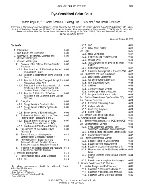
Dye-Sensitized Solar CellsAnders Hagfeldt,*,†,‡,|Gerrit Boschloo,†Licheng Sun,‡,|Lars Kloo,‡and Henrik Pettersson⊥Department of Physical and Analytical Chemistry,Uppsala University,Box259,SE-75105Uppsala,Sweden,Department of Chemistry,KTH-Royal Institute of Technology,Teknikringen30,SE-10044Stockholm,Sweden,State Key Laboratory of Fine Chemicals,DUT-KTH Joint Education and Research Centre on Molecular Devices,Dalian University of Technology(DUT),Dalian116012,China,and Swerea IVF AB,Box104,SE-43122Mo¨lndal,SwedenReceived October30,2009Contents1.Introduction65962.Sun,Energy,and Solar Cells65983.Overview of Performance,Materials,andOperational Principles65994.Operational Principles66024.1.Overview of the Different Electron-TransferProcesses66024.1.1.Reactions1and2:Electron Injection andExcited State Decay66034.1.2.Reaction3:Regeneration of the OxidizedDyes66034.1.3.Reaction4:Electron Transport through theMesoporous Oxide Film66034.1.4.Reactions5and6:Recombination ofElectrons in the Semiconductor withOxidized Dyes or Electrolyte Species66034.1.5.Reaction7:Reduction of ElectronAcceptors in the Electrolyte at the CounterElectrode66034.2.Energetics66034.2.1.Energy Levels in Semiconductors66044.2.2.Energy Levels of Redox Systems inSolution66054.2.3.Energy Levels of Excited Molecules66064.3.Photoinduced Electron Injection vs DirectRecombination-Reactions1and266074.3.1.Electron Injection Studies on ModelSystems:Dyes Adsorbed on TiO266074.3.2.Injection and DSC Device Efficiency66084.4.Regeneration of the Oxidized Dyes:Reaction366094.5.Electron Transport in MesoporousSemiconductor Electrodes:Reaction466104.6.Recombination of Electrons in theSemiconductor with Oxidized Dyes orElectrolyte Species:Reactions5and666124.7.Transport of the Redox Mediator and Reactionsat the Counter Electrode:Reaction766135.Materials Development66135.1.Nanostructured Metal Oxide Electrodes66135.1.1.TiO266145.1.2.ZnO66155.1.3.Other Metal Oxides6616 5.2.Dyes66165.2.1.Metal Complexes66175.2.2.Porphyrins and Phthalocyanines6620anic Dyes66235.2.4.The Anchoring of the Dye on the OxideSurface6631bining Sensitizers66325.2.6.Summary:Development of Dyes for DSC6632 5.3.Electrolytes and Hole Conductors66335.3.1.Liquid Redox Electrolytes66335.3.2.Gel and Polymer Electrolytes66345.3.3.Ionic Liquid Electrolytes66355.3.4.Additives66365.3.5.Alternative Redox Couples66365.3.6.Solid Organic Hole Conductors66375.3.7.Inorganic Solid Hole Conductors6638 5.4.Surface Passivation of Dye-Sensitized TiO26638 5.5.Counter Electrodes66395.5.1.Platinized Conducting Glass66395.5.2.Carbon Materials66395.5.3.Conducting Polymers66395.5.4.Cobalt Sulfide66395.6.Tandem Cells and p-Type DSCs66396.Characterization Techniques6641 6.1.Efficiency Measurements,I-V,IPCE,and APCE6641 6.2.Electrochemical Methods66426.2.1.Cyclic Voltammetry,Differential PulseVoltammetry,and Square Wave Voltammetry66426.2.2.Electrochemical Impedance Spectroscopy66426.2.3.Spectroelectrochemistry6642 6.3.Photoelectrochemical Methods66426.3.1.Electron Transport Measurements66426.3.2.Electron Lifetime Measurements66436.3.3.Electron Concentration Measurements66436.3.4.Measurements of the Electron Quasi-FermiLevel66446.3.5.Charge Collection Efficiency and DiffusionLength66446.3.6.Photoinduced Absorption Spectroscopy66447.Module Development/DSC Modules6645 7.1.Module Designs and Performance66457.1.1.Sandwich Z-Interconnected Modules66457.1.2.Sandwich W-Interconnected Modules66457.1.3.Sandwich Current-Collecting Modules6646*To whom correspondence should be addressed.E-mail:Anders.Hagfeldt@fki.uu.se.†Uppsala University.‡Royal Institute of Technology.|Dalian University of Technology(DUT).⊥Swerea IVF AB.Chem.Rev.2010,110,6595–6663659510.1021/cr900356p 2010American Chemical SocietyPublished on Web09/10/20107.1.4.Monolithic Serial-Connection Modules66477.1.5.Monolithic Current-Collecting Modules66477.2.Accelerated and Outdoor Module Testing66477.3.Manufacturing Processes66487.4.Discussion:Future Outlook for the DifferentDSC Module Designs66498.Future Outlook66509.Acknowledgments665110.Appendix.Content Added after ASAP Publication665111.Note Added after ASAP Publication665212.References6652 1.IntroductionAt the end of last century,the possibility to use devices based on molecular components for the construction of a robust large-scale solar electricity production facility seemed utopic.But the seminal paper by O’Regan and Gra¨tzel in 19911spurred researchers to take on the challenge.With the development of dye-sensitized solar cells(DSCs),2conven-tional solid-state photovoltaic technologies are now chal-lenged by devices functioning at a molecular and nanolevel. Record efficiencies of up to12%for small cells and about 9%for minimodules,promising stability data,passing,for example,the critical1000h stability test at80°C with a durable efficiency of8-9%,and means of energy-efficient production methods have been accomplished.The prospect of low-cost investments and fabrication are key features. DSCs perform also relatively better compared with other solar cell technologies under diffuse light conditions and at higher temperatures.DSCs offer the possibilities to design solar cells with a largeflexibility in shape,color,and transparency.Integration into different products opens up new commercial opportunities.Besides the exciting possibilities of using DSCs for solar energy application,the riddles of the device are as thrilling. How does it work?DSCs should according to the photo-voltaic textbooks in the early1990s simply not work.The paradigm was to use highly pure semiconductor materials avoiding defects and interfaces and to rely on a built-in electricalfield to separate photogenerated electron-hole pairs.DSCs,in contrast,were based on a huge internal interface prepared in a simple laboratory environment without strict demands on the purity of the materials.It was a mystery how the DSC could work in the absence of a built-in electric field.The initial research developed a relatively simple picture of how DSCs operate,reviewed in this journal in 1995.3The basic characteristics and conceptual models, reviewed in several recent articles,4-11have been reasonablysuccessful to describe various reactions and interactions.With time,however,the chemical complexity of the DSC device has become more and more evident.The DSC is a good example of a molecular system where the function of the overall device is better than predicted from the sum of the properties of its components.12There are complex interac-tions between the device components,in particular,at the oxide/dye/electrolyte interface,but the interactions also depend on external variables such as solar irradiation, temperature,and device working conditions.Also inherent in the devices are multiscaling properties,both in time and in length,which need to be characterized and handled for the optimization of the overall device performance.DSC research groups have been established around the world with biggest activities in Europe,Japan,Korea,China,and Australia.Thefield is growing fast,which can be illustrated by the fact that about two or three research articles are being published every day.In Figure1,a simple and limited literature search illustrates the growth of the number of research papers and patents over the last years.The industrial interest in DSCs is strong with large multinational companies such as BASF,Bosch,and Corus in Europe and Toyota,Sharp,Panasonic,Sony,Fujikura,and Samsung in Asia.A large volume production line has been set up in the company G24i,Wales.Research companies such as Dyesol,Australia,Solaronix,Switzerland,and Peccell,Japan,are expanding,focusing on selling material components and equipment.The principle of DSCs has also become a part of the core chemistry and energy science teaching and research.Text Anders Hagfeldt is professor in Physical Chemistry and the Dean of Chemistry at Uppsala University.He obtained his Ph.D.in1993at Uppsala University and was a postdoctoral fellow with Prof.Michael Gra¨tzel (1993-1994)at EPFL,Switzerland.His research focuses on physical chemical characterization of mesoporous electrodes for different types of optoelectronic devices,specifically dye-sensitized solar cells.He has about 200scientific publications and8patent applications.He is a member of the Royal Swedish Academy of Engineering Sciences(IVA),Stockholm, and a visiting professor at the Royal Institute of Technology,Stockholm, at Dalian University of Technology,China,and at the Institute for Materials Research and Engineering in Singapore.He is the director of Center for MolecularDevices.Gerrit Boschloo obtained his Ph.D.in1996at Delft University of Technology(The Netherlands).He held postdoctoral positions at University College Dublin(Ireland)with Prof.D.J.Fitzmaurice and at Uppsala University(Sweden)with Prof.Anders Hagfeldt.After a period as a researcher at the Royal Institute of Technology in Stockholm,he currently holds a position as an Associate Professor at the Department of Physical and Analytical Chemistry,Uppsala University.His main research interest is advanced photoelectrochemical characterization of dye-sensitized solar cells and nanostructured semiconductors.He is author of more than70 peer-reviewed articles.6596Chemical Reviews,2010,Vol.110,No.11Hagfeldt et al.books have sections or chapters dealing with DSC.13,14Laboratory kits have been developed for educational purposes under the slogan “make your own solar cell”.Not only energy science but also photochemistry,photoelectrochem-istry,materials science,and transition metal coordination chemistry have significantly benefitted from DSC research.The challenge to review the DSC research field is the speed of publications of new research data.With the risk of missing or leaving out interesting work,as well as studies ofimportance for the development of the field,we aim to cover the DSC research in a broad sense.We will,however,limit ourselves to sensitization by molecular dyes and will not discuss sensitization by semiconductor quantum dots.This topic was recently reviewed elsewhere.15,16After some brief notes on solar energy in general and DSC in particular (sections 2and 3),we go through theoperationalLicheng Sun obtained his Ph.D in 1990in Dalian University of Technology (DUT),China.After postdoctoral stays of one year (1992-1993)with Dr.Helmut Go ¨rner in Max-Planck-Institut fu ¨r Strahlenchemie,Mu ¨lheim an der Ruhr,Germany,and two years (1993-1995as Alexander von Humboldt fellow)with Prof.Dr.Harry Kurreck in Institut fu ¨r Organische Chemie,Freie Universita ¨t Berlin,he went to Stockholm first as an Assistant Professor (1995-1999)in Department of Chemistry,Royal Institute of Technology (KTH),and then Associate Professor (1999-2004)in Department of Organic Chemistry,Stockholm University.He moved back to KTH as a full Professor in Molecular Devices in 2004.He is now also a distinguished professor in DUT.His research interests focus on solar energy conversion at the molecular level including bioinspired systems for catalytic water oxidation and hydrogen production,artificial photosyn-thesis,dye-sensitized solar cells,supramolecular photochemistry,and light-driven water splitting.He has published more than 200peer-reviewedpapers.Lars Kloo received his Ph.D.in Inorganic Chemistry at Lund University,Sweden,in 1990and moved to his current position as Professor in Inorganic Chemistry at the Royal Institute of Technology (KTH)in Stockholm in 1998.During 1991-1995,he was in shorter or longer periods visiting scientist in other laboratories in the U.K.,U.S.A.,and New Zealand.He has been involved in DSC research for about 10years with a main focus on electrolytes,in particular ionic liquids,and more recently the electrolyte -electrode interaction.Apart from photoelectrochemical solar cells,his research interests also embrace fundamental aspects of inorganic synthesis,cluster chemistry,and computational biologicalchemistry.Henrik Pettersson is project leader at Swerea IVF AB,a research institute providing applied R&D to bring new technologies and new methods into practical applications.He has been involved in the development of dye-sensitized solar cells for more than 15years,specializing in module technologies,process methods,up-scaling,and reliability testing.Prior to joining Swerea IVF AB,he worked for Ekologisk Energi AB,one of the first companies to work on dye-sensitized solar cells,and for four years for Professor Michael Gra ¨tzel at EPFL inSwitzerland.Figure 1.Number of publications published per year obtained from a simple and limited literature search using the keywords “dye-sensitized”and “solar”:(a)number of research articles (data source,ISI Web of Knowledge);(b)number of patent families (data source,esp@cenet).Dye-Sensitized Solar Cells Chemical Reviews,2010,Vol.110,No.116597principles of DSC(energetics and kinetics)in section4.The development of material components is treated in section5 and some specific experimental techniques to characterize DSC in the following section.Section7deals with the current status of module development,andfinally we end up with a brief future outlook.2.Sun,Energy,and Solar CellsIt is clear that access to economically viable renewable energy sources is essential for the development of a globally sustainable society.The mean global energy consumption rate was13TW in the year2000.Assuming a kind of “business-as-usual”scenario with rather optimistic but reasonable assumptions of population growth and energy consumption,the projection is28TW in2050for the globalenergy demand.17,18Solar energy,besides fusion,has the largest potential to satisfy the future global need for renewable energy sources.19From the1.7×105TW of solar energy that strikes the earth’s surface,a practical terrestrial global solar potential value is estimated to be about600TW. Thus,using10%efficient solar farms,about60TW of power could be supplied.The sun emits light with a range of wavelengths from the ultraviolet and visible to the infrared.It peaks in the visible, resembling the spectrum of a blackbody at a temperature of 5760K.It is,however,influenced by atmospheric absorption and the position of the sun.Ultraviolet light isfiltered out by ozone,and water and CO2absorb mainly in the infrared making dips in the solar spectrum at900,1100,1400,and 1900nm(H2O)and at1800and2600nm(CO2).When skies are clear,the maximum radiation strikes the earth’s surface when the sun is directly overhead,having the shortest path length through the atmosphere.The path length is called the air mass(AM)and can be approximated by AM)1/cos , where is the angle of elevation of the sun.The standard solar spectrum used for efficiency measurements of solar cells is AM1.5G(global),giving that )42°.This spectrum is normalized so that the integrated irradiance(the amount of radiant energy received from the sun per unit area per unit time)is1000W m-2.The irradiance varies depending on the position of the sun,orientation of the Earth, and sky conditions.One also distinguishes sunlight in direct or diffuse light.The direct component can be concentrated, which increases the solar cell efficiency by increasing cell voltage outputs.Diffuse light arises by scattering of the sunlight in the atmosphere.This fraction is around15%on average20but larger at higher latitudes and in regions with a significant amount of cloud cover.Materials with rough surfaces such as DSCs are relatively better suited for diffuse light than perfectlyflat surfaces and are less sensitive to movements of the sun.The AM1.5G solar radiation spectrum can be found from different sources.21The spectrum is shown in Figure2as the irradiance of the sun as a function of wavelength.In the diagram,we also indicate the maximum current (short-circuit condition)for a solar cell device converting all incident photons below the absorption onset wavelength into electric current(see ref22).For example,the maximum short-circuit current(J sc)for a solar cell with an absorption onset of800nm is26mA cm-2.The overall solar-to-electrical energy conversion efficiency,η,for a solar cell is given by the photocurrent density measured at short-circuit (J sc),the open-circuit photovoltage(V oc),thefill factor of the cell(FF),and the intensity of the incident light(P in). Thefill factor can assume values between0and less than 1and is defined by the ratio of the maximum power(P max) of the solar cell per unit area divided by the V oc and J sc according toThe maximum power is obtained as the product of the photocurrent and photovoltage at the voltage where the power output of the cell is maximal.Another fundamental measure-ment of the performance of a solar cell is the“external quantum efficiency”,which in the DSC community is normally called the incident photon to current conversion efficiency(IPCE).The IPCE value corresponds to the photocurrent density produced in the external circuit under monochromatic illumination of the cell divided by the photon flux that strikes the cell.From such an experiment the IPCE as a function of wavelength can be calculated from where e is the elementary charge.IPCE values provide practical information about the monochromatic quantum efficiencies of a solar cell.Solar cell production has grown at about30%per annum over the past15years.The conventional solar cells of today, thefirst generation solar cells,are based on silicon.The estimated total installed capacity in2007was7.8GW.23,24 Most of this was grid-connected with a price of around$7 per peak Watt(W p).A selling price of$2/W p,which would correspond to a production cost of about$0.5/W p,would make PV competitive with electricity production from fossil fuels.Additional2.26GW was installed in2007alone(a 50%increase over the preceding year)and90%of that was installed in four countries:Germany,Spain,Japan,and the U.S.A.In2008,the worldwide photovoltaic installations increased by 6.0GW.However,the photovoltaic(PV) industry is largely dependent on governmental subsidies. Silicon-based systems make up around90%of the current PV market.The production cost is presently around$3/Wp Figure2.Photonflux of the AM1.5G spectrum at1000W m-2 (ASTM G173-03),and calculated accumulated photocurrent.η)JscVocFFPin(1)FF)P max/(J sc V oc)(2) IPCE)Jsc(λ)eΦ(λ))1240Jsc(λ)[A cm-2]λ[nm]P in(λ)[W cm-2](3)6598Chemical Reviews,2010,Vol.110,No.11Hagfeldt et al.but is highly dependent on the price of the silicon material. China is now the world leader in producing crystalline silicon (c-Si)based PV cells and modules with a capacity of over 2.3GW/year.The International Energy Agency(IEA)have estimated the energy payback time of c-Si PV modules, incorporated as a grid-connected roof-top installation,as between1.5and2years.25The second generation solar cells,for example,amorphous silicon,CIGS,and CdTe,are based on thinfilm technologies. They are becoming a competitive class of PVs,doubling production from2006to2007.The advantages of thinfilm solar cells include the ease of manufacture permitting a reduction of the production cost to about$1/W p,a wider range of applications with attractive appearance,and pos-sibilities of usingflexible substrates.The most established thin-film technology is amorphous silicon(a-Si).26The efficiencies are lower than c-Si,but it has other advantages such as a lower temperature coefficient for power loss.The cost is only slightly lower than that of c-Si mainly because of expensive manufacturing equipment.After an initial efficiency loss,the so-called Staebler-Wronski effect,stable laboratory efficiencies of13.5%and module efficiencies around5-6%have been achieved.For CdTe laboratory efficiencies of16.7%and module efficiencies of10.9%have been reported.The company First Solar has announced a production cost below$1/W p for their CdTe solar modules. The drawbacks include the toxicity and low abundance of the materials,temperature-dependent efficiencies,and only an average light tolerance.Nonetheless,CdTe is a highly interesting technology for future PVs.Another such technol-ogy is CIGS(copper indium gallium diselenide).CIGS systems are capable of high efficiencies(19.9%in the lab,27 16.7%in submodules,28and13.5%in modules.29They are very durable,and the materials cost can be kept low even though indium is rare.Since the bandgap can be tuned,they are also suitable for tandem cells.Several plants with10-50 MW capacity are now installed globally.Bothfirst and second generation solar cells are based on single junction devices.Calculated thermodynamic efficiency limits in single junction solar cells(31%)assume that absorption of an individual photon results in the formation of a single electron-hole pair and that all photon energy in excess of the energy gap is lost as heat.This so-called Shockley-Queisser limit can be overcome by the use of various types of so-called third generation solar cell devices.30 In principle,sunlight can be converted to electricity at an efficiency close to the Carnot limit of95%.Various schemes to achieve efficiencies above31%include tandem cells,hot carrier cells,multiexciton generation,multiband cells,and thermophotovoltaics.30The goal for the third generation solar cells is to deliver electricity at a large scale competitive price, that is,less than$0.5/W p.This means very effective solar cells that are produced by techniques that permit facile mass production.The impact on economics if such concepts could be implemented would be enormous,making PVs one of the cheapest options for future energy production.DSC can be considered to be a technology between the second and third generation solar cells.It has the potential to become a third generation technology utilizing the nanoscale properties of the device.In the present stage,the technology offers the following selling points:•low production cost and particularly interesting much lower investment costs compared with conventional PV technologies•design opportunities,such as,transparency and multi-color options(building integration,consumer products, etc.)•flexibility•lightweight•feedstock availability to reach terawatt scale•short energy payback time(<1year)•enhanced performance under real outdoor conditions (relatively better than competitors at diffuse light and higher temperatures)•bifacial cells capture light from all angles •outperforms competitors for indoor applications3.Overview of Performance,Materials,and Operational PrinciplesThe“Bob Beamon like”-increase in efficiency for DSC type solar cells reported in the famous1991Nature paper by O’Regan and Gra¨tzel was bewildering.The use of a mesoporous semiconductor electrode with a high internal surface area led to a paradigm shift in thefields of photoelectrochemistry and photovoltaics in general.Attempts to develop dye-sensitized photoelectrochemical cells had been made before,5,31-33but the basic problem was the belief that only smooth semiconductor surfaces could be used.The light-harvesting efficiency for a monomolecular layer of dye sensitizer,even for phhtalocyanines and porphyrins,which have among the highest extinction coefficients known,absorb far less than1%of the AM1.5G spectrum.34Attempts to harvest more light by using multilayers of dyes were in general unsuccessful.Indications of the possibilities to increase the roughness of the semiconductor surface so that a larger number of dyes could be adsorbed directly to the surface and simultaneously be in direct contact with a redox electrolyte had also been reported before1991.For example, Matsumura et al.35and Alonso et al.36used sintered ZnO electrodes to increase the efficiency of sensitization by rose bengal and related dyes.But the conversion yields from solar light to electricity remained well below1%for these systems. In addition,the dyes used in these systems were unstable. Gra¨tzel,Augustynski,and co-workers presented results on dye-sensitized fractal-type TiO2electrodes with high surface area in1985.37For DSC,there was an order-of-magnitude increase when O’Regan and Gra¨tzel in1991reported efficiencies of7-8%.1With regards to stability,a turnover number of5×106was measured for the sensitizer(a trimeric ruthenium complex38,39).This was followed up by the introduction of the famous N3dye(structure2in Table1) giving efficiencies around10%.40Since the initial work in the beginning of the1990s,a wealth of DSC components and configurations have been developed.Perhaps a key concept for the future success of DSC in this regard is“diversity”.At present,several thousands of dyes have been investigated,as well as hundreds of electrolyte systems and numerous types of mesoporous films with different morphologies and compositions.Whereas nature has over billions of years developed highly sophis-ticated molecular systems that give life on earth,chemists are at present facing the intriguing challenge of developing technologies based on complex molecular interactions that can assist in keeping the earth livable.Such technologies are expected to progress rapidly,be it through design of new materials based on fundamental insights or by statistical, combinatorial approaches.For DSC at present,in the official table of world record efficiencies for solar cells,the recordDye-Sensitized Solar Cells Chemical Reviews,2010,Vol.110,No.1165996600Chemical Reviews,2010,Vol.110,No.11Hagfeldt et al. Table1.Collection of Some Representative Ru-Complex Photosensitizersis held by the Sharp company in Japan at 10.4%(0.3%.41A criterion to qualify for these tables is that the solar cell area is at least 1cm 2.For smaller cells,a certified conversion efficiency of 11.1%has been reached using the black dye as sensitizer.42Early on in DSC research,the classical dyes N3and its salt analogue N719(structure 4in Table 1)and the black dye (N749,structure 3in Table 1)were developed.The certified record efficiencies are obtained with these dyes,and their IPCE spectra are shown together with the molecular structures of the dyes in Figure 3.22The IPCE values are close to 80%for both sensitizers across the visible part of the solar spectrum.The N3dye starts to absorb light at around 800nm,whereas the photocurrent onset is red-shifted for the black dye to 900nm.As seen from Figure 3,however,the IPCE increases only gradually from the absorption onset to shorter wavelengths due to relatively low extinction coefficients of these sensitizers.There is thus much to be gained by developing sensitizers with high extinction coefficients particularly in the near-IR region of the solar spectrum.The highest photocurrent densities of the black dye under AM 1.5G condition is close to 21mA cm -2,42,43which can be compared with the theoretical maximum photocurrent of 33mA cm -2from Figure 2for a dye with an absorption threshold of 900nm.Improving the solar light absorption in the 650-950nm domain (note the dip in the solar irradiance spectrum at 950nm,Figure 2)would then be one of the main directions to take aiming for DSC efficiencies above 15%.The other direction is to increase the photovoltage by replacing the conventionally used I -/I 3-redox couple with a system having a more positive redox potential.These are key challenges facing present DSC research and will be further discussed below.During the last 2-3years,the advent of heteroleptic ruthenium complexes furnished with an antenna function has taken the performance of the DSC to a new level.Two examples of these dyes are Z991and C101,structures 21and 28,respectively,in Table pared with the classical DSC Ru dyes,their extinction coefficients are higher and the spectral response is shifted to the red.The solar cellefficiency of these types of sensitizers has increased continu-ously over the last 2years,and at present efficiencies of 12%have been reported.22There are sometimes arguments that DSCs have not developed much since the breakthrough in the early 1990s.The record efficiencies reached a plateau at 10-11%,and the most efficient devices have remained essentially unchanged from its original concepts.It is,however,a complex system.The realization of the need to handling complexities with the plethora of material compo-nents to explore make the 12%efficiency now reached with one of the new classes of dyes a strong indicator for further progress in efficiency performance.Another essential per-formance indicator is long-term stability.Here,the progress during the last 15years has been steady,and accelerated durability tests have been passed with higher and higher efficiencies.Most of the earlier work has been reviewed.44-46As an example of recent results,the C101sensitizer maintains outstanding stability at efficiency levels over 9%under light soaking at 60°C for more than 1000h.47This is achieved by the molecular engineering of the sensitizer but also very importantly by the use of robust and nonvolatile electrolytes,such as ionic liquids,and adequate sealing materials.Good results on overall system endurance have been reported for several years,and these results are presently being confirmed under real outdoor conditions.Because of the direct relevance to the manufacturing of commercial products,little work is published on these issues,and it is,for example,difficult to find information on processing issues,as well as sealing materials and methods.The industrial development and commercialization of DSCs was the topic of the DSC-IC 3conference in Nara,Japan,April 2009.Many encouraging results were presented giving confidence that the DSCs can match the stability require-ments needed to sustain outdoor operation for many years.Still,many research and development activities need to be performed,and in particular,more data on outdoor field tests is required.One important research topic is to develop protocols for accelerated long-term stability tests relevant to DSC technologies.A schematic of the interior of a DSC showing the principle of how the device operates is shown in Figure 4.The typical basic configuration is as follows:At the heart of the device is the mesoporous oxide layer composed of a network of TiO 2nanoparticles that have been sintered together to establish electronic conduction.Typically,the film thickness is ca.10µm and the nanoparticle size 10-30nm in diameter.The porosity is 50-60%.The mesoporous layer is deposited on a transparent conducting oxide (TCO)onaFigure 3.Incident photon to current conversion efficiency as a function of the wavelength for the standard ruthenium sensitizers N3(red line),the black dye N749(black curve),and the blank nanocrystalline TiO 2film (blue curve).The chemical structures of the sensitizers are shown as insets.Reprinted with permission from ref 22.Copyright 2009American ChemicalSociety.Figure 4.Schematic overview of a dye-sensitized solar cell.Dye-Sensitized Solar Cells Chemical Reviews,2010,Vol.110,No.116601。

第53卷第5期2024年5月人㊀工㊀晶㊀体㊀学㊀报JOURNAL OF SYNTHETIC CRYSTALS Vol.53㊀No.5May,2024TOPCon 太阳电池单面沉积Poly-Si 的工艺研究代同光,谭㊀新,宋志成,郭永刚,袁雅静,倪玉凤,汪㊀梁(青海黄河上游水电开发有限责任公司西安太阳能电力分公司,西安㊀710100)摘要:目前隧穿氧化层钝化接触(TOPCon)电池制造技术越来越成熟,所耗成本不断降低㊂行业内普遍采用低压化学气相沉积(LPCVD)方式进行双面沉积或单面沉积㊂单面沉积存在Poly-Si 绕镀问题,严重影响电池片转化效率和外观质量,同时正面绕镀层去除难度较大,在用碱溶液去除绕镀层的同时,存在绕镀层去除不彻底或者非绕镀区域P +层被腐蚀的风险,导致P +发射极受损,严重影响电池片外观质量与性能㊂双面沉积可避免上述问题,但产能减少一半,制造成本增加㊂本文对单面沉积Poly-Si 工艺及绕镀层去除工艺进行研究,在TOPCon 电池正面及背面制作了一层合适厚度的氧化层掩膜,搭配合适的清洗工艺㊁去绕镀清洗工艺,既可有效地去除P +层绕镀的Poly-Si,也可很好地保护正面P +层及背面掺杂Poly-Si 层不受破坏,同时可大幅提升产能㊂关键词:TOPCon 太阳电池;Poly-Si 绕镀层;低压化学气相沉积;BSG;PSG;腐蚀速率中图分类号:TM914.4;TB43㊀㊀文献标志码:A ㊀㊀文章编号:1000-985X (2024)05-0818-06Single-Sided Deposition of Poly-Si in TOPCon Solar CellsDAI Tongguang ,TAN Xin ,SONG Zhicheng ,GUO Yonggang ,YUAN Yajing ,NI Yufeng ,WANG Liang (Xi an Solar Power Branch,QingHai Huanghe Hydropower Development Co.,Ltd.,Xi an 710100,China)Abstract :At present,the technology of tunnel oxide passivated contact (TOPCon)solar cells is becoming more and more mature,and the manufacturing cost is decreasing.TOPCon cell technology has been applied in the process of manufacture.Low-pressure chemical vapor deposition (LPCVD)is widely used in the industry for double-sided deposition or single-sided deposition.Single-sided deposition has the problem of Poly-Si winding coating,which seriously affects the efficiency and appearance quality of solar cells.It is difficult to remove the winding coating on the front side.While removing the winding coating in alkali solution,there is a risk of incomplete removal of the winding coating or corrosion risk of P +layer in non-winding plating area.As a result,the P +emitter is damaged,which seriously affects the appearance quality and performance of solar cells.Double-sided deposition can avoid the above risks,but the production capacity will be reduced by half,the manufacturing cost will increase.In this paper,the single-sided deposition of Poly-Si process and the removal process of the winding coating were studied.A layer of oxide coating with appropriate thickness is made on the front and back of TOPCon solar cells.With appropriate cleaning process and unwinding plating cleaning process,the Poly-Si winding coated with P +layer can be effectively removed,and the front P +layer and the doped Poly-Si layer on the back can be well protected from damage,and the production capacity can be greatly improved.Key words :TOPCon solar cell;Poly-Si winding coating;low pressure chemical vapor deposition;BSG;PSG;corrosion rate ㊀㊀收稿日期:2023-09-11㊀㊀作者简介:代同光(1986 ),男,山东省人,工程师㊂E-mail:tg334334@0㊀引㊀㊀言近年来,为应对能源危机和日益严重的环境问题,各国都在大力发展新能源,太阳能光伏发电技术因具有高效㊁清洁㊁取之不尽等优点,越来越受到国际能源产业的青睐㊂目前产业上应用最广泛的太阳能电池为传统晶硅电池,主要是以P 型单晶硅为衬底的钝化发射极背接触太阳电池(passivated emitterand rear cell,PERC)为主,但受P 型硅材料质量和器件结构设计的限制,其光电转化效率很难提高到23%以上[1]㊂而以N 型单晶硅片为衬底的N 型电池片,具有少子寿命高㊁对金属污染容忍度高㊁光致衰减低等㊀第5期代同光等:TOPCon太阳电池单面沉积Poly-Si的工艺研究819㊀优点,可用于制备双面电池,提高了太阳能电池系统的发电量,所以N型技术替代P型技术已成为光伏行业发展的趋势㊂在现有的N型电池中,隧穿氧化层钝化接触(tunnel oxide passivated contact,TOPCon)电池的隧穿氧化层和非晶硅层的沉积为硅片的背面提供了良好的表面钝化,提升了电池的开路电压和短路电流[2],TOPCon 电池具有工艺流程简单㊁效率提升空间大等优点,已被广泛应用于N型高效太阳能电池量产㊂TOPCon电池核心结构由SiO2隧穿氧化层和磷掺杂的多晶硅层组成,目前行业内TOPCon电池的制备方式主要为低压化学气相沉积(low pressure chemical vapor deposition,LPCVD)法[3]㊁等离子体增强化学气相沉积(plasma enhanced chemical vapor deposition,PECVD)法和溅射法,其中LPCVD技术制备的多晶硅膜层在片内及片间呈现较好的均匀性,电池端良率较高,工艺时间相对较短,生产效率高,同时LPCVD设备具有产能大㊁易于维护等优势,因此,LPCVD技术是目前TOPCon电池厂商布局的主流技术路线[4]㊂该技术采用LPCVD方式进行双面沉积或单面沉积,工艺的基本原理是将一种或数种气态物质,在较低压力下,用热能激活,使气态物质发生热分解或化学反应,沉积在衬底表面形成所需的薄膜㊂本征Poly-Si层的沉积主要应用硅烷的热分解来完成,在580~620ħ高温下,通入一定流量的硅烷,并将压力控制在一定范围内,硅烷热分解后在硅片表面沉积一定厚度的Poly-Si,化学反应式为SiH4ңSiˌ+2H2ʏ(1)其中单面沉积产能大但容易导致硅片正面边缘被绕镀Poly-Si(简称绕镀层),该绕镀层的存在影响电池正面对光的吸收,进而影响电池光电转换效率[5]㊂研究发现,与HF/HNO3酸刻蚀处理电池表面多晶硅绕镀相比,采用KOH碱刻蚀方法所处理的电池样品,在电池漏电流方面更具有优势[6],所以目前行业内普遍采用碱刻蚀去除绕镀层㊂但是碱溶液对前表面的腐蚀是全面的,也就导致前表面非绕镀区域也会受到影响,在去除绕镀层的同时,存在正面绕镀层去除不彻底或者非绕镀区域P+发射极被腐蚀的风险,严重影响电池片外观质量和性能㊂双面沉积可避免上述问题,但产能将减少一半,制造成本增加㊂为了保证单面沉积后电池的P+发射极在碱刻蚀过程中不被损坏,需要在P+发射极表面制备一层掩膜㊂本工作采用硼扩散时产生的硼硅玻璃(borosilicate glass,BSG)作为电池P+发射极掩膜,优点有:不增加新的生产设备,减少了电池制备成本;可通过调节硼扩散工艺实现P+发射极与BSG掩膜的共同制备,减少了电池制备流程,并避免样品转移过程带来的污染[6]㊂根据TOPCon电池工艺流程,在LPCVD后须对后表面进行磷掺杂㊂研究人员采用三氯氧磷热分解沉积方式进行磷掺杂,反应过程中生成的磷硅玻璃(phosphosilicon glass,PSG)被绕镀至硅片前表面,且绕镀的PSG厚度并不均匀,PSG的存在将影响Poly-Si绕镀层的去除,需要在去绕度工序前用HF 酸溶液去除㊂之前的研究人员通过实验发现,不同厚度的PSG叠加BSG,在HF酸溶液内的腐蚀速率不一致,进而影响前表面掩膜对P+发射极的保护作用㊂本文对单面沉积Poly-Si工艺及绕镀层去除工艺进行研究,通过在TOPCon电池正面及背面制备一层适宜厚度的氧化层掩膜,搭配刻蚀及去绕镀工序适宜浓度的清洗工艺,既可有效地去除P+层绕镀,也可很好地保护正面P+层及背面掺杂Poly-Si层不受破坏,解决Poly-Si绕镀层问题的同时,提高LPCVD产能㊂1㊀实㊀㊀验1.1㊀LPCVD单㊁双面Poly-Si沉积工艺对TOPCon电池外观及性能影响的实验在本公司TOPCon工艺产线其他工序工艺保持不变的条件下,LPCVD分别采用单插㊁双插方式制作电池,Poly-Si厚度120nm,对比LPCVD单㊁双面Poly-Si沉积时硅片前表面膜层结构的差异及LPCVD工艺后外观差异㊂1.2㊀LPCVD单㊁双面Poly-Si沉积时氧化层厚度对半成品外观影响的实验LPCVD采用单㊁双插方式制作电池半成品样片,在硼扩散㊁磷扩散工艺过程中,通过调整氧化压力,在硅片表面生长不同厚度的BSG㊁PSG,其他工序工艺保持不变,镀正面氮化硅后目测统计外观异常比例,实验设计如表1所示㊂820㊀研究论文人工晶体学报㊀㊀㊀㊀㊀㊀第53卷表1㊀不同氧化层厚度对单、双面Poly-Si 沉积TOPCon 太阳电池外观影响实验方案Table 1㊀Experimental scheme of effect of different oxide layer thickness on the appearance of single-sided anddouble-sided Poly-Si deposited TOPCon solar cellsLPCVDGroup Count Thickness of BSG /nm Thickness of PSG /nm G1-14008030Single-sideG1-240010040G1-340012050G2-14008030Double-side G2-240010040G2-3400120501.3㊀HF 酸溶液对不同厚度氧化层腐蚀速率影响的实验在上述实验硼扩散㊁磷扩散工艺过程中,同步使用碱抛光片在表面制备不同厚度的BSG㊁PSG㊁BSG +PSG,对比其在刻蚀HF 酸溶液内的腐蚀速率差异,实验设计如表2所示㊂表2㊀不同厚度氧化层在HF 酸内腐蚀速率实验方案Table 2㊀Experimental scheme of corrosion rate comparison in HF acid for different oxide layer thicknessOxide layer Thickness /nm Concentration of HF /%Time /s BSG 80 1.5120PSG 50 1.512080+30 1.5120BSG +PSG80+40 1.512080+50 1.51201.4㊀Poly-Si 厚度及绕镀面积对单面Poly-Si 沉积TOPCon 电池外观影响的实验LPCVD 采用双插方式制作电池半成品样片,通过调整LPCVD 沉积时间得到不同厚度的Poly-Si,其他工序工艺保持不变,镀膜后统计外观异常比例㊂1.5㊀实验过程实验材料:N 型金刚线切割硅片制绒后半成品若干㊁N 型金刚线切割硅片抛光片若干㊁HF 酸溶液㊂图1㊀TOPCon 电池制备工艺路径Fig.1㊀Preparation process path of TOPCon cells 实验设备及仪器:深圳捷佳创湿法槽式清洗设备㊁深圳捷佳创低压扩散设备㊁普乐LPCVD㊁RENA InOxSide 链式刻蚀机㊁深圳捷佳创管式镀膜设备㊁Syscos COSE PV4.0光谱椭偏仪㊂实验方法:取N 型金刚线切割硅片制绒后半成品若干,使用深圳捷佳创低压扩散设备进行硼扩散工艺,通过调整氧化压力制备不同厚度的BSG,硼扩后的样品按实验组进行分类,经RENA链式刻蚀机清洗背表面及侧边横截面的BSG 后,浸没在捷佳创湿法槽式设备NaOH 刻蚀槽中对背表面进行抛光,再使用普乐LPCVD 设备进行单㊁双面Poly-Si 沉积,之后在深圳捷佳创低压扩散设备进行磷扩散工艺,通过调整氧化压力制备不同厚度的PSG,后流转至去PSG 工序,使用RENA 链式刻蚀机清洗前表面绕镀Poly-Si 上层绕扩PSG,进一步在去绕镀清洗工序使用深圳捷佳创湿法槽式NaOH 刻蚀溶液去除绕镀Poly-Si,最后使用深圳捷佳创管式镀膜设备对硅片前表面镀氮化硅膜,实验结束后全检外观,统计半成品外观情况㊂上述硼扩散㊁磷扩散过程中,同步使用NaOH 碱刻蚀抛光后的硅片作为氧化层厚度监控片,并随样品进行流转,用于去PSG 工序监控氧化层厚度变化㊂实验样品制作工艺流程如图1所示㊂㊀第5期代同光等:TOPCon太阳电池单面沉积Poly-Si的工艺研究821㊀2㊀结果与讨论2.1㊀LPCVD单、双面Poly-Si沉积工艺对TOPCon电池结构及外观的影响当LPCVD采用双面沉积(单槽单插)时,硅片正表面㊁背面均沉积厚度一致的Poly-Si,硅片前表面颜色均匀㊂采用单面沉积(单槽双插)时,硅片背面沉积厚度一致的Poly-Si,硅片正面绕镀厚度不一致的Poly-Si,根据前表面外观颜色可以看出,从硅片边缘到中心,绕扩的多晶硅厚度呈递减趋势,单双面沉积P+层绕镀结构对比如图2所示㊂LPCVD工艺前和工艺后半成品前表面外观如图3所示㊂图2㊀LPCVD单面与双面结构图Fig.2㊀Structure of single-sided and double-sided by LPCVD图3㊀LPCVD单面与双面P+层外观Fig.3㊀P+layer appearance of single-sided and double-sided by LPCVD2.2㊀LPCVD单面Poly-Si沉积时氧化层厚度对半成品外观影响经实验数据分析(见表3)可知,LPCVD采用双面沉积时,样品镀膜后外观无异常㊂LPCVD采用单面沉积时,当硼扩散BSG厚度小于80nm时,在BOE去绕镀时不足以保护P+层,导致部分区域被腐蚀抛光;当BSG厚度大于100nm时,抛光现象消除;当PSG厚度大于40nm时,在BOE去绕镀时P+层局部被过度腐蚀导致外观发白的比例最高;当PSG厚度小于40nm时,发白比例随PSG厚度减小而递减㊂外观正常及异常图片如图4所示㊂表3㊀LPCVD单面与双面匹配不同厚度氧化层的外观数据Table3㊀Appearance data of single-sided and double-sided by LPCVD matching with different oxide layer thickness LPCVD Group Proportion of polishing/%Proportion of whiten/%G1-110 Single-side G1-200.5G1-30 1.5G2-100 Double-side G2-200G2-3002.3㊀HF酸溶液对不同掺杂氧化层腐蚀速率的影响HF酸对不同厚度氧化层腐蚀能力数据如图5所示㊂从图中可以看出,不同氧化层在同一浓度HF酸溶液内的腐蚀速率为:V BSG<V PSG<V BSG+PSG㊂在腐蚀BSG+PSG叠层掩膜时,随着PSG厚度的增加,腐蚀速率将增大,而在磷扩工艺过程中,P+层绕镀的PSG厚度是不一致的,这将导致刻蚀在去除P+层PSG绕镀时,腐822㊀研究论文人工晶体学报㊀㊀㊀㊀㊀㊀第53卷蚀速率不一致,部分区域剩余掩膜较薄,在去绕镀时被腐蚀,被腐蚀区域比表面积变小,在镀氮化硅膜时,同一条件下,反应气体流量相同,比表面积大的区域沉积的氮化硅厚度越小,而比表面积小的区域则反之[7],导致被腐蚀区域膜厚异常,外观呈发白状,所以在选择磷扩散工艺时,要尽量降低P +层绕扩的PSG 厚度,以降低BSG +PSG 叠层掩膜在刻蚀的腐蚀速率差异㊂图4㊀LPCVD 单面经去绕镀㊁镀膜后的外观Fig.4㊀Appearance after dewinding and coating of single-side by LPCVD图5㊀HF 酸对不同厚度氧化层腐蚀能力数据Fig.5㊀Etching ability data of HF acid to different oxide layers thickness 2.4㊀改进效果评估综上所述,通过在TOPCon 电池前表面制备适宜厚度的BSG 掩膜,同时控制PSG 厚度,可有效解决单面Poly-Si 沉积导致的外观异常,同步制作两组改进前和改进后的电池片进行对比,统计前表面外观异常比例和电性能参数,评估改进效果,实验条件及结果如表4所示㊂实验结果显示,改进前外观抛光比例1.2%,外观发白比例1.8%,改进后外观无明显异常㊂改进前外观异常区域PN 结被腐蚀破坏,难以产生光生伏特效应,导致转化效率损失,改进后外观无异常,电池性能显著提升㊂表4㊀不同厚度氧化绕镀层对单面Poly-Si 沉积TOPCon 太阳电池外观及电性能影响Table 4㊀Effects of different oxide layer thickness on the appearance and electrical properties of TOPCon solar cells deposited by single-sided Poly-SiGroup Count Thickness of BSG /nm Thickness of PSG /nm U oc /V I sc /AR s /ΩR sh /ΩFF /%NCell /%Proportion of polishing /%Proportion of whiten /%Baseline 40080500.706513.69140.0009460282.6624.27 1.2 1.8Improvement 400100300.707413.69950.0008466582.7824.32003㊀结㊀㊀论1)在TOPCon 工艺过程中,LPCVD 采用单面Poly-Si 沉积时,前表面非绕镀区域在清洗去绕镀时容易被腐蚀,导致电池片外观异常㊁效率损失㊂㊀第5期代同光等:TOPCon太阳电池单面沉积Poly-Si的工艺研究823㊀2)氧化层厚度对TOPCon电池外观起着至关重要的作用,当硼扩散BSG厚度小于一定量时,在BOE去绕镀时不足以保护P+层,导致部分区域被腐蚀抛光;PSG厚度大于一定厚度时,在BOE去绕镀时P+层局部易被过度腐蚀导致发白㊂3)各掺杂氧化层在刻蚀HF酸溶液内的腐蚀速率为:V BSG<V PSG<V BSG+PSG㊂在腐蚀BSG+PSG叠层掩膜时,随着PSG厚度的增加,腐蚀速率将增大㊂4)通过在TOPCon电池正面制备一层适宜厚度的氧化层掩膜,搭配刻蚀及去绕镀工序化学品1.5%浓度的清洗工艺,即可有效地去除P+层绕镀的Poly-Si,也可很好地保护正面P+层不受破坏,解决单面沉积Poly-Si 外观异常的同时,提高LPCVD产能㊂参考文献[1]㊀张㊀志.隧穿氧化层钝化接触(TOPCon)太阳电池的研究[D].昆明:昆明理工大学,2019.ZHANG Z.Research on tunneling oxide passivation contact(TOPCon)solar cells[D].Kunming:Kunming University of Science and Technology,2019(in Chinese).[2]㊀肖友鹏,李桂金.硅太阳电池钝化载流子选择性接触概念与现状[J].电源技术,2019,43(11):1897-1900.XIAO Y P,LI G J.Concept and present situation of passive carrier selective exposure in silicon solar cells[J].Chinese Journal of Power Sources,2019,43(11):1897-1900(in Chinese).[3]㊀SACHS E,PRUEGER G,GUERRIERI R.An equipment model for polysilicon LPCVD[J].IEEE Transactions on SemiconductorManufacturing,1992,5(1):3-13.[4]㊀王举亮,贾永军.LPCVD法制备TOPCon太阳能电池工艺研究[J].人工晶体学报,2023,52(1):149-154.WANG J L,JIA Y J.Preparation of TOPCon solar cells by LPCVD method[J].Journal of Synthetic Crystals,2023,52(1):149-154(in Chinese).[5]㊀张㊀婷,刘大伟,宋志成,等.多晶硅绕镀层的去除工艺研究[J].人工晶体学报,2020,49(9):1641-1645.ZHANG T,LIU D W,SONG Z C,et al.Research on surround coating removal technology for polysilicon[J].Journal of Synthetic Crystals, 2020,49(9):1641-1645(in Chinese).[6]㊀周㊀颖.n型隧穿氧化层钝化接触太阳电池的量产关键问题研究[D].大连:大连理工大学,2021.ZHOU Y.Study on key Issues in mass production of N-type tunneling oxide passivation contact solar cells[D].Dalian:Dalian University of Technology,2021(in Chinese).[7]㊀涂宏波,马㊀超,王学林,等.晶硅太阳电池氮化硅膜产生色差的影响因素研究[J].化工中间体,2013,10(5):37-41.TU H B,MA C,WANG X L,et al.The inluence factors causing color diference of silicon nitride film of crystalline silicon solar cell[J].Chemical Intermediates,2013,10(5):37-41(in Chinese).。


THIRD GENERATION BIPVSTANDARD BUILDING ELEMENTS WITH INTEGRATED PHOTOVOLTAICClaas HelmkeUnited Solar Ovonic Europe GmbHTrakehner Strasse 7 – 9, 60487 Frankfurt, GermanyT: +49.69.7137667 0, F: T: +49.69.7137667 67, chelmke@ABSTRACT: First generation building integrated photovoltaic, BIPV, systems consisted of PV modules mounted onto private or commercial buildings using custom-made substructures and fixtures. Second generation BIPV systems were systems where PV elements were replacing parts of the building envelope and partially taking over its functions. With the commercial availability of flexible PV elements the third generation of BIPV systems uses standard building elements, which come with integrated flexible PV modules. The first section of this paper describes the production of flexible photovoltaic PV modules made from amorphous silicon and demonstrates their specific advantages. These modules employ triple-junction amorphous silicon solar cells, which are deposited on a stainless steel substrate. In the second section of this paper, the evolution of building integrated PV systems is demonstrated.A precondition for growth in the BIPV segment is the availability of new designs for BIPV modules, overcoming traditional obstacles seen in previous generations of BIPV systems. The aim is to pave the way for reliable, functional, cost effective and statically viable BIPV systems for roofs of industrial buildings by use of flexible thin film amorphous silicon solar modules, which are shaped into standard building elementsKeywords: Building Integration; Thin Film; Cost Reduction1 WORKING PRINCIPLE AND PRODUCTION OFFLEXIBLE PV MODULESUnited Solar Ovonic LLC has developed and refined unique production technology for thin-film amorphous silicon solar cells. In a roll-to-roll process three amorphous silicon solar cells are deposited onto a stainless steel substrate [1]. In production, six coils of stainless steel, each 2500 m long, 36 cm wide and 0.125 mm thick, are put through one manufacturing process, integrating the following four production steps:1.washing of stainless steel substrate2.back reflector deposition (Al and ZnO)3.amorphous silicon alloy deposition4.anti-reflective coating (indium tin oxide, ITO)Figure 1: 25 MWp production facilityFigure 1 shows the amorphous silicon alloy deposition machine where the triple junction solar cell deposition occurs. The machine is approximately 100 m long and has an annual production capacity of 25 MWp.Nine layers of a-Si and a-SiGe alloys are deposited, resulting in three solar cells stacked on top of each other. The three cells have a different spectral responsivity; the bottom cell absorbs the red light, the middle cell the green/yellow light and the top cell absorbs the blue light. This spectrum splitting capability is one of the keys to higher efficiencies and higher energy output, especially at low irradiance conditions and/or high ratio of diffused light [2].After the deposition processes have been completed, the following production steps are then employed to create the United Solar Ovonic PV modules, laminates and other building-integrated products:1.cutting of stainless steel substrate into slabs2.short passivation and cell definition3.bonding of electrodes4.cutting of cells5.cell and by-pass diode connectionmination7.performance and wet hi-pot test, visual inspectionThe cell strings are encapsulated in UV-stabilized, weather-defying polymers. This laminating process incorporates EVA and the fluoro-polymer, ETFE on the top side. Bypass diodes are connected across each cell allowing the modules to produce power even when partially shaded. Standard size of PV laminates for BIPV applications is 5.5 m x 0.4 m or 2.85 m x 0.4 m, with a nominal power of 136 Wp and 68 Wp respectively. Significant advantages of this technology and the laminate design are:•flexibility•low weight (2,2 kg/m²)•small temperature coefficient of power (-0,21%/K) •fully walkable roof•good integration into ridged or flexible building elements•Shadow tolerant (each solar cell is connected via a by-pass diode)•Annual energy yield is less dependent on optimal orientation and inclination of array2 THE EVOLUTION OF BUILDING INTEGRATEDPHOTOVOLTAIC SYSTEMSEver since PV modules became commercially available a fraction is used being mounted onto buildings. From a today perspective the solutions found were not always in favour of the design of the building. Often it seams that solar pioneers think that the main reason to have a roof on a building is to put a solar PV array on it. The following chapters outline some critical observations on BIPV system design and come to a PV solution employing standard building elements to serve the primary reason for roofs: water tightness.2.1 First generation of BIPV systemsFirst generation of building integrated photovoltaic systems are systems where the photovoltaic generator is mounted onto an existing roof. In residential systems thePV modules are mounted in parallel to the roof surface.Figure 2: First generation residential BIPV systemOn roofs of commercial building, which are usually flat, modules are mounted at a desired tilt angle using a dedicated substructure. For the introduction of PV in buildings this was an adequate approach. However, the questionable appearance of these roof-mounted generators and issues of quality (both in product and in workmanship), needed to be addressed:2.1.1 Remarkable additional weightMounting a solar array on existing residential buildings is normally not a problem because the typical residential substructure is built for heavy snow and is capable of supporting the framed solar modules and mounting structure. However, when working on commercial building it is absolutely important that the addition of more weight on the roof be carefully evaluated, especially when it comes to old and/or light-framed agricultural buildings. Additional weight loads can be substantial. For example, a common method for mounting framed modules on a commercial roof is through the use of plastic troughs, which are filled with gravel or equivalent to secure the array to the roof. This technique can be used so as to avoid damaging the roof by drilled holes to fix a mounting structure. With such systems additional weight of up to 100 kg/m² can be reached, which need to be supported by the (existing) roof structure.2.1.2 Additional wind loadsAdditional wind loads emerge almost always, when additional components are mounted onto a roof. Even if solar modules are mounted in parallel to the roof the edges are exposed to wind and remarkable loads may beintroduced into the roof structure. Relevant punctual forces need to be evaluated carefully in terms of their impact on the static of the building. This impact is most obvious looking at elevated mounted PV systems on flat roofs of commercial buildings. The occurring stress introduced into the building structure depends on the height of the building and the average local wind speed and is determined according to building codes and standards, following to which the building needs to be statically analysed. But, even the most accurate calcula-tions can not prevent extraordinary wind velocities. Due to the elevation of the modules, they operate like sails and catch the wind. The fixture of the PV plant should be designed in such a way that under heavy wind conditions the PV system is sacrificed and may fly away, as first of all the integrity of the roof needs to be ensured. The economical damage due to a damaged roof might bemuch higher than the loss of the PV system.Figure 3: First generation commercial BIPV system2.1.3 Damage of the building envelopeThe majority of buildings have roofs that prevent any possibility that water penetrates the building. Wilfully damaging the water-tight surface of the building by drilling holes to fasten the PV array contradicts the primary function of the roof, water tightness. Today solutions for mounting systems which promise everlasting water-tightness of drilled holes are available, but with large installations the principle question of reasonability should be raised.2.1.4 Principle definition of interface building/PV systemThe following questions need to be answered in the event of damage, when it comes to reimbursement of costs:• Who did what?• Was he entitled to do the job? • Did he have the right training?The roofer lays the roof, the solar company installs the PV system, and the electrician connects the PV system to the grid. Upon completion water penetrates the roof. Questions are:• Who caused the damage? • Who repairs the roof?• Who covers the costs for repair?• Who covers the related costs inside the building, likedamaged goods stored there, which might well be significant?2.1.5 MaintenanceRoofs of commercial buildings have usually a title angel of 2-5°. If an elevated PV system is mounted onsuch a roof, maintenance is more complicated and draining of rain and snowmelt is constricted.2.2 The second generation of BIPV systemsSecond generation BIPV systems are characterised by the fact that PV modules replace parts of the buildingenvelope and thus take over parts of its function.Figure 4: 2nd generation residential BIPV systemFigure 5: 2nd generation commercial BIPV systemIt is necessary and good that PV modules become multi-functional; which lowers their relative costs. If this development shall proceed in a sustainable way, the primary function of the building envelope, the protection from the outside climate, may not be neglected.If this function is not satisfactorily provided by the PV modules, than this kind of systems will not gain any market share. Further points of observation are:2.2.1 No usage of standard productsA key to reduce costs is the use of standard building elements and/or solutions. This is valid as well for BIPV systems, but most of the PV modules employed in second generation BIPV systems are tailor-made. Beyond higher prices for non-standard products this fact has consequences resulting from building laws. Due to the utilisation of non-standard products no Building Code certification is available for the use as a building element, which might significantly complicates the approval process of the building as such.2.2.2 Interdisciplinary engineeringIt has been observed that some module manufactures start designing BIPV module without sufficient background knowledge concerning the construction of parts for buildings. The fulfilment of requested primary functions of parts such as water tightness, sound reduction, and thermal separation prove to be challenges in such circumstances.2.2.3 Responsibilities and warranteeThe above explanation explains why the module manufacturer has to take over the warranty for the module to comply with principle requirements on primary functions of the building envelope. This implies high financial risks.2.2.4 Temperature performanceDue to the integrated mounting of BIPV modules these devices operate at higher temperatures than PV modules mounted so that air can flow below them. Higher operating temperature lowers the power output of PV devices and complicates the system sizing. Above mentioned points need to be considered during the design steps of the entire system layout its electrical layout. Further they increase total system costs and/or pay-back time of the system.2.3 Third generation of BIPV systemsSince 1998 United Solar Ovonic manufactures flexible photovoltaic laminates on a commercial scale.Figure 6: United Solar Ovonic flexible PV laminateThese laminates are integrated into standard building elements by selected manufacturers of building elements. Standard industrial building elements for roofs can be made from a variety of materials like steel (with or without incorporated isolation material), zinc-titanium, aluminium, and flexible, non-metallic roofing membranes. These selected partner companies developed a new end-product, based on their standard roofing product, combined with Uni-Solar laminates, which is certified according IEC 61646 to ensure durability, and in certain countries to make them eligible for funding same as ‘normal’ PV modules). Advantages of this technology in BIPV applications are: • High degree of pre-fabrication• Clear definitions of responsibilities on the roof• Little additional weight and no additional wind loads • Use of traditional building/roofing elements with allapplicable certification according to building codes and regulations to ensure water tightness• Much smaller temperature coefficient than crystallinesilicon PV cells• Roof remains walkable for maintenance• Non-optimal orientation and inclination has smallesteffect on energy yield• PV system installation equals normal roofing workand procedure• Roofer ensures water tightness of roofThe following figures show some examples of PV projects realised by partner companies of United Solar Ovonic. All projects have in common that the Uni-Solar laminates are directly and entirely bonded to the roofing elements. The roof structure keeps a homogeneous appearance due to the use of identical roofing elements with or without photovoltaic elements, where their application makes no sense.•Figure 7 displays the ThyssenKrupp-Solartec product, a metal pan with insulation layer, 1 m wide and up to 24 meter long•Figure 8 displays a single ply roofing membrane system created by Alwitra, using the Alwitra Evalon Solar product•Figure 9 displays a system made from aluminium standing seam profiles, which can be used as well ina rounded shape•Figure 10 displays a roofing membrane system created by Solar Integrated, using the Sarnafil roofing membraneFigure 7: ThyssenKrupp-SolartecFigure 8: Alwitra Evalon Solar3 SUMMARYWith the development of flexible photovoltaic laminates United Solar Ovonic contributes remarkably to the evolution of building integrated photovoltaic systems. With the possible integration of flexible PV elements into standard building and roofing elements new options for BIPV applications are created, which lead to increased product reliability, product security and reduction of total system costs. Additionally, due to the specific characteristics of the Uni-Solar laminates, new fields of applications can be realised. This accounts in particular to buildings with weak statically properties (weight, wind load), or where the owner entertains concerns against elevated PV-glass systems.United Solar Ovonic is responding to an increasing demand for their flexible PV laminates with an expansion plan to increase capacity to over 300 MWp by the year 2010.Figure 9: Kalzip AluPlusSolarFigure 10: Solar Integrated3.1 References1 S. Guha, J. Yang, A. Banerjee, K. Hoffman, S.Sugiyama, J. Call, S. J. Jones, X. Deng, J. Doehler, M. Izu, and H.C. Ovshindky, “Triple-junction amorphous silicon alloy PV manufacturing plant of 5 MWp annual capacity”, 26th IEEE PVSC, New York, USA, 1997, p. 6072. M. van Cleef, P. Lippens, J.Call - Bekaert ECD SolarSystems Europe N.V.- BESS EUROPE SuperiorEnergy Yields of UNI-SOLAR® Triple JunctionThin Film Silicon Solar Cells compared toCrystalline Silicon Solar Cells under Real OutdoorConditions in Western Europe.Thanks to T. Parker for extensive discussion and review.。
Steve ByrnesDecember 2008NSE 290 Schottky junction solar cellsA photovoltaic cell can be created from the Schottky junction between a semiconductor and a metal, with or without an insulating layer between them. Solar cells of this type have a long history, dating back to 1883, when Charles Fritts coated selenium with a thin layer of gold to make one of the world’s first solar cells. However, since then, they have commanded only a small amount of attention from researchers and corporations; no popular solar-cell design uses metals in the active region, other than for contacts. Nevertheless, in the past decade or two, university research and an industrial pilot production line have demonstrated the potential commercial viability of one particular Schottky junction solar cell design, the silicon “MIS-IL solar cell” (short for metal-insulator-semiconductor inversion-layer), and moreover they continue to be used fairly commonly in a lab setting (due to their simple architecture). In this paper, we will examine the general operating principles of Schottky junction solar cells, with particularly emphasis on the MIS-IL design of primary commercial interest.1 Background on Schottky barriersAs discussed in class, an interface between a metal and semiconductor can induce a depletion or inversion layer in the semiconductor. (It can also induce an accumulation layer, but this case is not of interest for this paper.) A built-in potential called the “Schottky barrier” appears between the bulk of the semiconductor and the surface. The magnitude of the potential is called the “Schottky barrier height” (SBH). As discussed in class, for a perfect abrupt junction between the metal and semiconductor, the Schottky-Mott model gives the SBH in terms of the electron affinity of the semiconductor, the work-function of the metal, and the band gap. For a p-type semiconductor,SBH = (band gap) + (electron affinity) – (work function)while for an n-type semiconductor,SBH = (work function) – (electron affinity)In reality, however, the SBH is not described well by the Schottky-Mott model, because of interface states and defects.Similar to this is the MIS (metal-insulator-semiconductor) junction, wherein a thin insulator (a few nanometers, typically) is inserted between the metal and semiconductor. The insulator functions as a tunnel barrier, allowing electrons and holes to tunnel through with some finite probability. In the Schottky-Mott model, the insulator lowers the barrier height very slightly, because some of the electric field drop occurs across the insulator, rather than between the surface of the semiconductor and the bulk. However, since the insulating layer tends to be much thinner than the depletion region, the potential drop is small and the effect is negligible. Experimentally, on the other hand, the SBH is often significantly larger in an MIS than in the analogous MS structure, contrary to the Schottky-Mott model.12 IV characteristicsAcross an MS or MIS barrier, there are two types of current paths. In the “minority carrier current path”, a minority carrier passes between the metal and the semiconductor (through the insulator, if there is one). The “majority carrier current path” is analogous.2.1 Minority carrier current pathThe minority carrier current path is essentially the same as in a p-n junction, but instead of achieving the junction through a change in doping, you achieve it through the inversion or depletion layer induced by the metal. As always, the current goes in both directions. In the reverse direction, there is a generation current from electron-hole pairs generated in or near the depletion region either thermally (in the dark) or from photons (in the light). In the forward direction, there is the recombination current from majority carriers diffusing into the depletion region, then recombining. The net dark current, as with a normal p-n junction, isI = I0,minority (Exp(eV/kT)–1).2.2 Majority carrier current pathThe majority carrier current path is not present in a p-n junction. Here, the majority carrier from the bulk semiconductor goes to or from the metal, without ever involving minority carriers.The main contribution to reverse dark current (majority carriers moving from the metal to the semiconductor) is Schottky-Richardson emission (also called “Thermionic emission”). Here, the carriers in the metal randomly have enough energy to pass over the barrier height. The magnitude of this current is reasonably constant with respect to applied voltage, since the energy barrier from the metal to the semiconductor is reasonably constant, unlike the energy barrier from the semiconductor to the metal, which reduces markedly in forward bias.The constant reverse-current is balanced by a forward current consisting of majority carriers being thermally excited over the Schottky barrier. On net, we get the classic diode equation:I = I0,majority (Exp(eV/kT)–1).Note that this is a somewhat simplified picture. The full electrostatics of the MIS system, including image-charge lowering,2 field emission,2 interface-state dynamics, and so forth, means it does not satisfy the classic diode equation, but rather can have large ideality factors, non-saturating reverse current, and other complications.3,42.3 Effect on solar-cell performanceSummed up, we get a typical diode characteristic, with saturation current I0=I0,minority+I0,majority. High saturation current hurts solar-cell performance, and therefore the “extra” majority-carrier current path is detrimental to the net efficiency. This is the main justification for inserting an insulating layer: A tunnel barrier of the correct thickness (typically a few nanometers) can reduce I0,majority, without appreciably lowering the short-circuit current, which involves minority carriers tunneling through the insulator. The reason for the asymmetry is that the electric field drives theminority carriers towards the barrier, where they can pile up to a certain degree while waiting to tunnel through. The majority carriers, on the other hand, are being driven away from the interface by the electric field, so slowing their passage can dramatically reduce their net flow.53 MIS-IL CellsThe most important realization of Schottky barrier solar cells today is the “MIS-IL solar cell,” made from single-crystalline (SC) silicon. The processing sequence for a standard (or “first-generation”) MIS-IL solar cell is as follows:6,7 First, the top surface is textured mechanically and chemically. Second, the back aluminum contact is evaporated on. Third, there is a heating stage, which simultaneously sinters the Al and grows a 1.5nm SiO2 thermal oxide. Fourth, the front aluminum grid is mask-evaporated. Finally, the structure is dipped in CsCl, and then a SiN x layer is deposited on the front side by PECVD. The SiN x layer passivates the surface, reducing recombination, functions as an antireflective coating, and moreover its interface states and charges are such that it creates an inversion layer in the silicon. The CsCl dip incorporates Cs+ ions, increasing the density of positive charges in the SiN x, and hence the strength (and therefore conductivity) of the inversion layer.8One key difference with the standard solar-cell process is the lack of a high-temperature phosphorus-diffusion step, which ordinarily creates the n-layer of the p-n junction. The elimination of this step is advantageous for two reasons: First, the energy input into the solar-cell production process is 35% lower,9 which lowers production cost and the energy-payback-period for the cell. Second, the crystal defects and high doping of the diffused layer tends to increase saturation current due to SRH and Auger recombination, respectively. Lacking this layer, the MIS-IL cell can achieve a larger-than-usual open-circuit voltage, as high as 655 mV in SC-silicon in an early 1979 cell.10 On the other hand, while the lack of the diffusion step is an advantage of MIS-IL cells on high-quality SC-silicon, it is a disadvantage on low-quality Si, since there the high-temperature diffusion step improves crystal quality by gettering impurities.4 Commercial Status and ProspectsFrom 1994, >1 MW p of “first-generation” MIS-IL cells were manufactured in an industrial pilot plant.9 These cells showed an efficiency of 15.3% for 10x10cm2 CZ-Si crystals, and 15.7% for2x2cm2 FZ-Si. However, ongoing research has uncovered substantial room for improvement in the process. The best current approach is “OECO-MIS-IL” solar cells.11 (OECO stands for “obliquely evaporated contacts”.) The key advantages of this technique are, first, the mask-evaporation step, which was found to be difficult to scale up, is eliminated, being replaced by the OECO metal-grid-deposition technique; and second, the SiN x passivation layer can be deposited at a higher temperature, creating better passivation. (In a first-generation MIS-IL cell, increasing the SiN x deposition temperature would degrade the MIS contacts; in the new processing sequence, the metal is deposited after the SiN x.) These cells have 19.6% record efficiency. This efficiency is for a lab cell, but it is claimed that it was created using only cheap, industrially-scaleable processes, and moreover with much room for further improvement.In conclusion, MIS-IL solar cells are a promising candidate for the future of high-end SC-Si solar cells, offering distinct advantages in cost and efficiency. However, one should keep in mindthat there are a large number of new, innovative, and advantageous SC-Si solar cell architectures, and it is beyond the scope of this paper to state where MIS-IL solar cells stand among all the great contenders in today’s marketplace. Nevertheless, it will be exciting to see the results of this research effort, which continues both in the laboratory and in pilot plants.References:1 M. Green, Solar Cells. Australia: University of New South Wales Press, 1998. Especially see sections 9.4 and 9.6.2 S.M. Sze, Physics of Semiconductor Devices. New York: Wiley, 19693 H.C. Card and E H Rhoderick, J. Phys. D4, 1589 (1971).4 D.L. Pulfrey, IEEE Trans. Electron. Devices25, 1308 (1978).5 H.C. Card, Solid St. Electron.20, 971 (1977).6 T. Markvart and L. Castañer, Practical Handbook of Photovoltaics. New York: Elsevier, 2003. Section 3.3.7 Grauvogl et al., IEEE 25th PVSC, 433 (1996).8 R. Hezel et al., J Electrochem. Soc.131, 1679 (1984).9 R. Hezel, Prog. Photovoltaics Res. App.5, 109 (1997).10 Godfrey and Green, App. Phys. Lett.34 790 (1979)11 R. Hezel, Solar En. Mat. Solar Cells74, 25 (2002)。
第53卷第2期2024年2月人㊀工㊀晶㊀体㊀学㊀报JOURNAL OF SYNTHETIC CRYSTALS Vol.53㊀No.2February,2024全TOPCon 电池正面多晶硅层硼掺杂工艺张㊀博1,宋志成1,2,倪玉凤1,魏凯峰1(1.青海黄河上游水电开发有限责任公司西安太阳能电力分公司,西安㊀710000;2.西安电子科技大学微电子学院,宽禁带半导体材料与器件教育部重点实验室,西安㊀710071)摘要:为提升隧穿氧化层钝化接触(TOPCon)电池光电转换效率,本文通过高温扩散在n 型TOPCon 电池正面制作p 型隧穿氧化层钝化接触结构,提升发射极钝化性能,减少正面金属复合㊂本文研究了不同沉积时间㊁推进温度㊁推进时间等工艺参数对实验样品钝化性能及掺杂曲线的影响㊂实验结果表明,当沉积时间为1500s,推进温度为920ħ,推进时间为20min 时,掺硼多晶硅层可获得较优的钝化性能及掺杂浓度,其中样品多晶硅层硼掺杂浓度达到1.40ˑ1020cm -3,隐开路电压(i V oc )大于720.0mV㊂依据该参数制备的TOPCon 电池光电转换效率可达23.89%,对应的短路电流密度为39.36mA /cm 2,开路电压(V oc )达到726.4mV,填充因子(FF)为83.54%㊂关键词:TOPCon 电池;钝化接触;硼扩散;钝化;电流密度;光电转换效率中图分类号:TM914.4㊀㊀文献标志码:A ㊀㊀文章编号:1000-985X (2024)02-0329-07Boron Doping Technology for the Front Polysilicon Layer of Full TOPCon CellsZHANG Bo 1,SONG Zhicheng 1,2,NI Yufeng 1,WEI Kaifeng 1(1.Xi an Solar Power Branch,Qinghai Huanghe Hydropower Development Co.,Ltd.,Xi an 710100,China;2.Key Laboratory of Wide Bandgap Semiconductor Materials and Devices,Ministry of Education,School of Microelectronics,Xidian University,Xi an 710071,China)Abstract :In order to improve the efficiency of tunneling oxide passivated contact (TOPCon)cells,a p-type tunneling oxide passivation contact structure was fabricated on the front of N-type TOPCon cells through high-temperature diffusion,improving the emitter passivation performance and reducing front metal recombination.The effects of different deposition time,drive-in temperature,drive-in time and other process parameters on the passivation performance and doping curve of experimental samples were investigated.The experimental results show that when the deposition time is 1500s,the drive-in temperature is 920ħ,and the drive-in time is 20min,the boron doped polysilicon layer can achieve better passivation performance and boron doping concentration,with the doping concentration of sample polycrystalline silicon layer reaching 1.40ˑ1020cm -3.The implied open circuit voltage(i V oc )is greater than 720.0mV.The photoelectric conversion efficiency of TOPCon cells prepared based on this parameter can reach 23.89%,corresponding to a short-circuit current density of 39.36mA /cm 2,the open circuit voltage (V oc )is 726.4mV,and the fill factor (FF)is 83.54%Key words :TOPCon cell;tunnel oxide passivation contact;boron diffusion;passivation;current density;photoelectric conversion efficiency ㊀㊀收稿日期:2023-08-14㊀㊀作者简介:张㊀博(1987 ),男,陕西省人,工程师㊂E-mail:zhangbo02@0㊀引㊀㊀言n 型隧穿氧化层钝化接触(N-type tunneling oxide passivated contact,N-TOPCon)太阳电池是目前市场上光电转换效率较高的晶硅太阳电池之一,其理论极限光电转换效率为28.7%,接近单结晶硅太阳电池的极限光电转换效率(29.43%)[1]㊂从产业发展来看,N-TOPCon 电池技术因独特的电池结构及较高的光电转换效率,成为市场关注的焦点㊂2014年,德国弗劳恩霍夫太阳能研究所Feldmann 等[2]首次提出了隧穿氧化层钝化接触(tunnel oxide330㊀研究论文人工晶体学报㊀㊀㊀㊀㊀㊀第53卷passivated contact,TOPCon)电池的概念,其主要特征是在n型硅片背面先利用化学法制备一层超薄氧化硅层,然后沉积一层掺杂多晶硅层,两者共同形成钝化接触结构作为电池背面钝化层㊂由于钝化接触特殊的能带结构,n型重掺杂多晶硅与n型硅衬底接触,使n型硅衬底能带向下弯曲,降低了电子传输势垒,因此超薄氧化层可允许多子电子隧穿而阻挡少子空穴透过,从而使电子和空穴分离,减少了复合,在n型重掺杂多晶硅上沉积一层金属作为电极就实现了无须开孔的钝化接触结构[3-5]㊂目前国内TOPCon电池已经开始产业化生产,其中晶科能源产业化的产品光电转换效率超过25.4%[6],另外2023年4月10日中来光电在自主研发的TOPCon3.0技术和M10尺寸n型电池片的基础上,实现了高达26.7%的电池片实验室光电转换效率,创造了目前n型TOPCon电池光电转换效率的世界纪录[7]㊂目前量产的n型TOPCon电池均为背面隧穿钝化接触结构,电池正面仍采用传统的单晶结构,存在钝化低㊁金属复合高㊁接触电阻大等缺点,根据Long等[8]的研究成果,单面TOPCon电池极限光电效率只有27.1%,要想达到28.7%的极限光电效率需制作全TOPCon电池结构㊂由于多晶硅层对光的寄生吸收,在电池前表面制作整面TOPCon结构会严重影响光吸收,导致短路电流严重降低,电池光电转换光电效率下降㊂解决方案之一是在金属栅线位置制作一种与栅线宽度相似的钝化接触结构,称为钝化接触栅线[9] (passivated contact polysilicon-finger,Poly-finger),可在减少金属复合的同时尽可能减少光吸收损失㊂本文通过对不同的扩散工艺进行研究,在实验样品表面制作对称的p型钝化接触结构并进行表征测试,获得较优的掺杂工艺后在常规n型单面TOPCon电池正面制作Poly-finger结构,将单面TOPCon电池升级为全TOPCon 电池,提升了电池效率㊂1㊀实㊀㊀验1.1㊀实验方案在整个硼扩散过程中,硼源流量㊁沉积时间㊁沉积温度,以及推进时间㊁推进温度都会影响硼的掺杂浓度及分布曲线,根据高嘉庆等[10]的研究结果,硼源流量选用100mL/min,沉积温度选择830ħ作为基础工艺条件,通过研究不同沉积时间㊁扩散时间与扩散温度获得p型TOPCon结构最佳硼掺杂工艺,并根据最佳工艺参数制备全TOPCon太阳电池㊂样品的钝化表征主要依据饱和电流密度J0和隐开路电压i V oc㊂J0指的是硅片高掺杂区域的复合程度,但如果表面能进行有效钝化处理,便可以降低其复合程度,J0也会随之下降;i V oc主要体现硅片整体少子寿命情况,计算公式[11]为[](1)i V oc=KT q lnΔn(Δn+N dop)n2i式中:Δn为过剩载流子密度,N dop为施主或受主原子浓度,K为玻尔兹曼常数,T为热力学温度,n i为本征载流子浓度,q为电荷量㊂根据计算公式,i V oc与Δn成正比,i V oc越高说明少子寿命越长,钝化效果越好㊂本文主要研究了不同沉积时间(500㊁1000㊁1500㊁2000s)㊁不同推进温度(880㊁900㊁920㊁960ħ)㊁不同推进时间(20㊁30㊁40min)对Poly-finger结构钝化性能和硼掺杂分布的影响,并基于实验结果进一步研究了不同硼掺杂工艺对全TOPCon电池I-V性能的影响㊂1.2㊀样品制备本实验选用n型硅片,电阻率为3~7Ω㊃cm,尺寸为166mmˑ166mm,硅片少子寿命不小于1ms㊂由于Poly-finger宽度较窄,本次实验样品选择整面掺杂方式方便表征测试,结构为双面对称的pn结+双面隧穿氧化层+硼掺杂多晶硅层+氮化硅层㊂首先使用碱溶液去除硅片表面切割损伤层形成抛光面,然后使用低压化学气相沉积(low pressure chemical vapor deposition,LPCVD)设备沉积隧穿氧化层及多晶硅层,再使用扩散炉进行不同工艺的硼掺杂,掺杂后使用1%的氢氟酸溶液浸泡清洗去除表面硼硅玻璃(borosilicate glass, BSG),清洗后抽取部分样品进行硼掺杂浓度分布曲线测试,对剩余样品进行双面镀氮化硅膜以及高温烧结,最后完成J0及i V oc测试㊂其中去损伤层单面腐蚀厚度为3~5μm,隧穿氧化层设计厚度为1.8nm,掺硼多晶硅层设计厚度为150nm,氮化硅膜层厚度为65~70nm㊂㊀第2期张㊀博等:全TOPCon电池正面多晶硅层硼掺杂工艺331㊀实验样品及Poly-finger结构如图1所示㊂图1㊀实验样品(a)及Poly-finger(b)结构示意图Fig.1㊀Structure diagram of experimental sample(a)and Poly-finger(b)1.3㊀测试与表征使用ECV测试仪(WEP Wafer Profiler CVP21,德国)测试硼掺杂分布情况㊂采用准稳态光电导(QSSPC)寿命测试仪(WCT-120,Sinton Instruments,美国)分别测量每组样品的钝化性能,包括J0和i V oc㊂对最终的TOPCon电池,I-V曲线等特性都是通过瞬态模拟器测试,并且在I-V测试之前须对AMG1.5太阳光谱进行校准,同时补偿探针阴影的误差㊂2㊀结果与讨论2.1㊀沉积时间对样品掺杂曲线及钝化性能的影响根据隧穿氧化钝化接触结构的钝化机理,较高的多晶硅层硼掺杂浓度会有效提升场钝化效果,同时还会降低金属电极与多晶硅层的接触电阻,有利于提升电池转换效率[12-13]㊂图2是沉积温度为830ħ㊁不同沉积时间下硼掺杂曲线及钝化性能测试结果,从图2(a)中可以看出,多晶硅层硼掺杂浓度随着沉积时间增加而增加,各组掺杂浓度分别为8.80ˑ1019㊁1.02ˑ1020㊁1.35ˑ1020㊁1.40ˑ1020cm-3,当沉积时间增加到1500s 时多晶硅层掺杂浓度不再继续提升,这是由于硼在硅中固溶度较低,随着多晶硅层硼掺杂浓度提升,硼源无法更多地进入多晶硅层㊂从图2(b)中可以看出,不同沉积时间对应的样品钝化性能无明显差异,这是由于沉积温度为830ħ时,硼原子无法通过隧穿层进入硅基体形成p+层,进而无法实现载流子选择,因此钝化性能偏低㊂图2㊀不同沉积时间硼掺杂分布(a)及钝化情况(b)Fig.2㊀Boron doping distribution(a)and passivation(b)for different deposition time2.2㊀推进温度对样品掺杂曲线及钝化性能的影响为了在N型硅片上实现p型TOPCon结构需要在硼沉积后增加硼推进步骤,根据2.1小节结果,为保证多晶硅层掺杂浓度,硼沉积时间设定为1500s,推进时间设定为10min㊂图3为不同推进温度下硼掺杂分布332㊀研究论文人工晶体学报㊀㊀㊀㊀㊀㊀第53卷及钝化性能测试结果㊂实验结果表明,当推进温度为880ħ时,多晶硅层掺杂浓度约为8.87ˑ1019cm-3,对应i V oc为702.2mV,J0为20.0fA/cm2;当温度在900和920ħ时样品钝化性能相似,且920ħ时i V oc达到最大值,此时样品多晶硅层硼掺杂浓度约1.10ˑ1020cm-3,对应的i V oc分别为714.3㊁715.1mV,饱和电流J0分别为19.8㊁15.1fA/cm2;当推进温度达到960ħ时虽然表面硼掺杂浓度提高到1.50ˑ1020cm-3,但是高温破坏了隧穿氧化层,同时硅基体界面处俄歇复合增加[14]导致i V oc降到690.8mV,同时J0增至38.5fA/cm2㊂图3㊀不同推进温度下硼掺杂分布(a)㊁钝化效果(b)和饱和电流密度(c)曲线Fig.3㊀Boron doping distribution(a),passivation effect(b),and saturation current density(c)at different drive-in temperatures 2.3㊀推进时间对样品掺杂曲线及钝化性能的影响影响样品钝化性能的因素包括扩散温度及扩散时间,由2.2小节实验结果可知最佳扩散温度为920ħ,故将本次实验推进温度设定为920ħ,通过对比不同推进时间对样品掺杂曲线及钝化性能的影响,确定最优的工艺条件㊂图4为920ħ下不同推进时间对应的硼掺杂分布及钝化性能测试结果㊂从图4(a)可以看出,当扩散时间分别为20㊁30㊁40min时,对应的多晶硅层硼掺杂浓度从1.40ˑ1020cm-3减小到1.03ˑ1020cm-3,结深由0.22μm增加到0.28μm,这是由于随着推进时间增加,多晶硅层的硼原子被推入硅基体造成多晶硅层掺杂浓度减小㊂由于表面硼掺杂浓度降低,多晶硅层场钝化效应减弱,同时掺入基体的硼原子浓度增加,硅基体载流子复合速率提升[14],对应的i V oc从720.0mV下降到706.0mV,J0从10.0fA/cm2增加到27.3fA/cm2㊂2.4㊀电池制备与测试根据以上实验得出的硼掺杂参数,进行全TOPCon电池小批量制备,工艺流程如图5所示㊂制备的TOPCon电池正面为Poly-finger结构,单根设计宽度为100μm,钝化层为氧化铝+氮化硅;背面使用扩散进行磷掺杂,结构为隧穿氧化层+磷掺杂多晶硅层+氮化硅层㊂电池结构[15]及能带结构如图6所示㊂表1中G1~G5组为不同硼掺杂参数的TOPCon太阳电池的电性能参数,G6组为常规单面TOPCon电池参数,表中n为样品数量,η为平均光电转换效率,FF为填充因子,J sc为短路电流密度,T为扩散推进温度,D为扩散推进时间㊂㊀第2期张㊀博等:全TOPCon电池正面多晶硅层硼掺杂工艺333㊀图4㊀920ħ下不同推进温度下硼掺杂分布(a)㊁钝化效果(b)和饱和电流密度(c)曲线Fig.4㊀Boron doping distribution(a),passivation effect(b),and saturation current density(c)for different drive-in time at920ħ图5㊀电池工艺流程示意图Fig.5㊀Process schematic diagram of cells图6㊀全TOPCon太阳电池结构(a)㊁能带示意图(b)和Poly-finger外观(c)Fig.6㊀Full TOPCon solar cells structure(a),energy band diagram(b),and Poly-finger appearance(c)334㊀研究论文人工晶体学报㊀㊀㊀㊀㊀㊀第53卷表1㊀使用不同硼掺杂参数制备的TOPCon太阳电池电性能数据Table1㊀Electrical performance data of TOPCon solar cells fabricated with different boron doping parameters Sample T/ħD/min V oc/mV J sc/(mA㊃cm-2)FF/%η/%nG188010713.439.3381.1622.77191G292010721.039.3183.0723.54195G396010705.239.2880.1322.19194G492020726.439.3683.5423.89187G592030722.139.2483.1723.56188G6 713.441.2082.5124.21200表1中,G1~G5组电性能参数反映了全TOPCon电池光电转换效率受硼掺杂参数的影响趋势㊂可以看出,当扩散温度为920ħ,扩散推进时间为20min时,全TOPCon电池获得了最高的平均光电转换效率,达到23.89%,J sc为39.36mA/cm2其中开路电压V oc达到726.4mV,较常规单面TOPCon电池提升13mV以上,FF为83.54%㊂G6组为常规单面TOPCon电池的电性能数据,从电流密度对比数据可以看出,正面栅线下方增加Poly-finger后,平均电流密度下降了2mA㊃cm-2,导致本次实验中全TOPCon电池光电转换效率低于单面TOPCon电池㊂电流密度下降的主要原因有:1)为了简化制备流程㊁提升钝化性能,Poly-finger结构设计为抛光面,且多晶硅层厚度未进行减薄优化,从而影响了光吸收;2)为保证印刷质量,制备的Poly-finger宽度为100μm,而细栅宽度仅为30μm,增加了光的寄生吸收㊂但从V oc㊁FF等电性能数据可以看出,Poly-finger结构有助于提升电池钝化效果,降低金属复合,改善接触电阻,有效提升TOPCon电池的V oc和FF,为后续电池的光电转换效率提升提供支持㊂3㊀结㊀㊀论1)通过实验研究,最佳工艺参数为:沉积时间为1500s,扩散温度为920ħ,推进时间为20min㊂此时多晶硅层掺杂浓度可控制在1.40ˑ1020cm-3,对称结构i V oc可达到720.0mV㊂2)在最优工艺参数下,小批量制备的全TOPCon电池平均光电转换效率达到23.89%,对应的短路电流密度为39.36mA/cm2,开路电压为726.4mV,FF为83.54%㊂通过本文的研究,全TOPCon电池发射极钝化性能和接触性能得到了保证,虽然电流密度较常规单面TOPCon电池下降2mA㊃cm-2左右,但后续通过优化Poly-finger宽度,减小多晶硅厚度,引入绒面结构等改善措施,可进一步减少电流损失,提升全TOPCon电池的光电转换效率㊂参考文献[1]㊀陈俊帆,赵生盛,高㊀天,等.高效单晶硅太阳电池的最新进展及发展趋势[J].材料导报,2019,33(1):110-116.CHEN J F,ZHAO S S,GAO T,et al.High-efficiency monocrystalline silicon solar cells:development trends and prospects[J].Materials Reports,2019,33(1):110-116(in Chinese).[2]㊀FELDMANN F,BIVOUR M,REICHEL C,et al.Passivated rear contacts for high-efficiency n-type Si solar cells providing high interfacepassivation quality and excellent transport characteristics[J].Solar Energy Materials and Solar Cells,2014,120(1):270-274.[3]㊀RICHTER A,BENICK J,FELDMANN F,et al.N-type Si solar cells with passivating electron contact:identifying sources for efficiencylimitations by wafer thickness and resistivity variation[J].Solar Energy Materials and Solar Cells,2017,173:96-105.[4]㊀TAO Y G,UPADHYAYA V,JONES K,et al.Tunnel oxide passivated rear contact for large area n-type front junction silicon solar cellsproviding excellent carrier selectivity[J].AIMS Materials Science,2016,3(1):180-189.[5]㊀PEIBST R,LARIONOVA Y,REITER S,et al.Implementation of n+and p+poly junctatom on front and rear side of double-side contactedindustrial silicon solar cells[C]32nd European Photovoltaic Solar Energy Conference and Exhibition.Munich,Germany,2016:323-327.[6]㊀佚㊀名.晶科能源系列新品闪耀亮相上海SNEC2023展会[EB/OL].(2023-05-24)[2023-08-08].https:///site/newsdetail/1549.ANONYMITY.Jinkosolar series new products shine at SNEC2023exhibition in Shanghai[EB/OL].(2023-05-24)[2023-08-08].https:// /site/newsdetail/1549(in Chinese).[7]㊀佚㊀名.26.7%!中来刷新n型TOPCon电池世界最高效率![EB/OL].(2022-04-11)[2023-08-08]./NewsDetails-436-1442.html.㊀第2期张㊀博等:全TOPCon电池正面多晶硅层硼掺杂工艺335㊀ANONYMITY.26.7%!To refresh the N-type TOPCon battery with the world's highest efficiency![EB/OL].(2022-04-11)[2023-08-08]./NewsDetails-436-1442.html(in Chinese).[8]㊀LONG W,YIN S,PENG F G,et al.On the limiting efficiency for silicon heterojunction solar cells[J].Solar Energy Materials and Solar Cells,2021,231:111291.[9]㊀叶继春.TOPCon电池低成本化和高效化发展路径探索[C]//第十八届中国太阳级硅及光伏发电研讨会(18th CSPV)论文集,2022:2615-2640.YE J C.Exploration of low-cost and high-efficiency development paths for TOPCon cells[C].18th China SoG Silicon and PV Power Conference, 2022:2615-2640(in Chinese).[10]㊀高嘉庆,郭永刚,屈小勇,等.n型IBC太阳电池选择性发射极工艺研究[J].人工晶体学报,2022,51(11):1929-1935.GAO J Q,GUO Y G,QU X Y,et al.Study on selective emitter technology of n-type IBC solar cell[J].Journal of Synthetic Crystals,2022,51(11):1929-1935(in Chinese).[11]㊀张㊀志.隧穿氧化层钝化接触(TOPCon)太阳电池的研究[D].昆明:昆明理工大学,2019:26-26.ZHANG Z.Study on tunnel oxide passivation contact(TOPCon)solar cells[D].Kunming:Kunming University of Science and Technology, 2019:26-26(in Chinese).[12]㊀PADHAMNATH P,WONG J,NAGARAJAN B,et al.Metal contact recombination in mono Poly TM solar cells with screen-printed&fire-throughcontacts[J].Solar Energy Materials and Solar Cells,2019,192:109-116.[13]㊀WU Y,STODOLNY M K,GEERLIGS L J,et al.In-situ doping and local overcompensation of high performance LPCVD polysilicon passivatedcontacts as approach to industrial IBC cells[J].Energy Procedia,2016,92:427-433.[14]㊀马㊀典.高质量p型隧穿氧化硅钝化接触及其在高效晶硅太阳电池的应用[D].昆明:云南大学,2022.MA D.High-quality p-type tunneling silicon oxide passivation contact and its application in high-efficiency crystalline silicon solar cells[D].Kunming:Yunnan University,2022(in Chinese).[15]㊀杨㊀露,刘大伟,倪玉凤,等.一种N型TOPCon太阳能电池及其制作方法:CN115036384A[P].2022-09-09.YANG L,LIU D W,NI Y F,et al.A N-type TOPCon solar cell and its production method:CN115036384A[P].2022-09-09(in Chinese).。
Published:May 12,2011COMMUNICATION /JACSInterface-Directed Assembly of One-Dimensional Ordered Architecture from Quantum Dots Guest and Polymer HostShengyang Yang,Cai-Feng Wang,and Su Chen*State Key Laboratory of Materials-Oriented Chemical Engineering,and College of Chemistry and Chemical Engineering,Nanjing University of Technology,Nanjing 210009,P.R.ChinabSupporting Information ABSTRACT:Assembly of inorganic semiconductor nano-crystals into polymer host is of great scienti fic and techno-logical interest for bottom-up fabrication of functional devices.Herein,an interface-directed synthetic pathway to polymer-encapsulated CdTe quantum dots (QDs)has been developed.The resulting nanohybrids have a highly uniform fibrous architecture with tunable diameters (ranging from several tens of nanometers to microscale)and enhanced optical performance.This interfacial assembly strategy o ffers a versatile route to incorporate QDs into a polymer host,forming uniform one-dimensional nanomaterials po-tentially useful in optoelectronic applications.Similar to the way that atoms bond to form molecules and complexes,inorganic nanoparticles (NPs)can be combined to form larger ensembles with multidimensional ordered hier-archical architecture,evoking new collective functions.To this end,the development of the controlled self-assembly method for well-de fined structures of these ensembles is signi ficant for creating new and high-performance tunable materials and hence has aroused appealing scienti fic and industrial interest.1Particu-larly,much e ffort has been devoted to the construction of one-dimensional (1D)structures of NPs,owing in part to their application as pivotal building blocks in fabricating a new generation of optoelectronic devices.2In this context,directed host Àguest assembly of NPs into polymer matrices is an e ffective “bottom-up ”route to form 1D ordered functional materials with advantageous optical,electrical,magnetic,and mechanical properties.3Some typical routes have been developed for the generation of these 1D hybrids so far,involving template-assisted,4seeding,5and electro-static approaches.6However,the challenge still remains to precisely manipulate assembly of aqueous NPs and water-insoluble polymers into uniform 1D nanocomposites with a high aspect ratio because of phase separation and aggregation.7Moreover,facile synthetic strate-gies are highly needed to fabricate homogeneous 1D composites in which each component still preserves favorable properties to produce optimal and ideal multifunctional materials.A liquid Àliquid interface o ffers an ideal platform to e fficiently organize NPs into ordered nanostructures driven by a minimiza-tion of interfacial energy.8While much of this research has been directed toward NP hybrids with diverse morphologies based on small organic ligand-directed assembly,9some success has also been achieved in polymer-based NPs nanocomposites.10Russelland co-workers developed ultrathin membranes and capsules of quantum dots (QDs)stabilized by cross-linked polymers at the toluene/water interface.10a,11Brinker ’s group reported the fab-rication of free-standing,patternable NP/polymer monolayer arrays via interfacial NP assembly in a polymeric photoresist.12Herein,a simple host Àguest assembly route is developed to facilely create homogeneous 1D CdTe/polymer hybrids without any indication of phase separation at the aqueous/organic inter-face for the first time.The CdTe nanocrystal is a semiconductor that has been used extensively for making thin film for solar cells.13Some elegant studies have been made in synthesizing pure inorganic 1D CdTe nanowires via assembly from corre-sponding individual CdTe nanocrystals.14In this work,CdTe QDs are covalently grafted with poly(N -vinylcarbazole-co -glycidylmethacrylate)(PVK-co -PGMA)to form uniform fibrous fluorescent composites at the water/chloroform interface via the reaction between epoxy groups of PVK-co -PGMA and carboxyl groups on the surface of CdTe QDs (Scheme 1).15These 1D composite fibers can be allowed to grow further in the radial direction by “side-to-side ”assembly.Additionally,this type of interfacial QD Àpolymer assembly can observably improve the fluorescence lifetime of semiconductor QDs incorporated in theScheme 1.Schematic Representation of the Synthesis of PVK-co -PGMA/CdTe QDs Composite Nano fibersReceived:February 8,2011polymeric matrix.It can be expected that this example of both linear axial organization and radial assembly methodology can be applied to fabricate spatial multiscale organic Àinorganic com-posites with desired properties of NPs and polymers.Figure 1a shows a typical scanning electron microscope (SEM)image of PVK-co -PGMA/CdTe QDs composite nano fi-bers obtained at the water/chloroform interface after dialysis.The as-prepared fibers have uniform diameters of about 250nm and typical lengths in the range of several tens to several hundreds of micrometers (Figures 1a and S4Supporting In-formation [SI]).Interestingly,PVK-co -PGMA/CdTe composite fibers can randomly assemble into nestlike ring-shaped patterns (Figures 1b and S5[SI]).Given the interaction among epoxy groups,the formation of nestlike microstructures could be attributed to incidental “head-to-tail ”assembly of composite fibers.Moreover,in order to establish the relationship between the role of epoxy groups and the formation of composite nano fibers,control experiments were performed,in which pure PGMA or PVK was used to couple CdTe QDs.The PGMA/CdTe composites could be obtained with fibrous patterns (Figure S6[SI]),but no fibrous composites were achieved at the biphase interface with the use of PVK under the same conditions.The microstructures and fluorescence properties of PVK-co -PGMA/CdTe composite fibers were further character-ized using laser confocal fluorescence microscopy (LCFM).Confocal fluorescence micrographs of composite fibers show that the di fferently sized QDs have no obvious in fluence on the morphology of composites (Figure 1c Àe).Clearly,uniform and strong fluorescence emission is seen throughout all the samples,and the size-dependent fluorescence trait of CdTe QDs in PVK-co -PGMA matrix remains well.In order to verify the existence and distribution of CdTe QDs in the fibers,transmission electron microscopy (TEM)was employed to examine the assembled structures.Figure 2a shows a TEM image of PVK-co -PGMA/CdTe QDs composite nano fi-bers,indicating each composite fiber shown in Figure 1a was assembled from tens of fine nano fibers.An individual fine nano fiber with the diameter of about 30nm is displayed in Figure 2b,from which we can see that CdTe QDs have been well anchored into the fiber with polymeric protection layer,revealing this graft-form process at the interface e ffectively avoidednon-uniform aggregation in view of well-dispersed CdTe QDs within the composite fiber,consistent with the LCFM observa-tion.Unlike previous works where the nanoparticles were ad-sorbed onto the polymer fibers,16CdTe QDs were expelled from the surface of fibers (∼2.5nm)in our system (Figure 2c),albeit the high percentage of QDs in the polymer host (23wt %)was achieved (Figure S7[SI]).This peculiarity undoubtedly confers CdTe QDs with improved stability.The clear di ffuse rings in the selected area electron di ffraction (SAED)pattern further indicate excellent monodispersion and finely preserved crystalline struc-ture of QDs in the nano fibers (Figure 2d).The SAED data correspond to the cubic zinc blende structure of CdTe QDs.A possible mechanism for the assembly of 1D nanostructure was proposed,as illustrated in Figure S8[SI].The hydrophilic epoxy groups of the PVK-co -PGMA chain in the oil phase orient toward the biphase interface and then react with carboxyl groups on the surface of CdTe QDs in the aqueous phase to a fford premier PVK-co -PGMA/CdTe QDs composites.Such nanocomposites will reverse repeatedly,resulting from iterative reaccumulation of epoxy groups at the interface and the reaction between the active pieces (i.e.,epoxy or carboxyl groups)in the composites with intact CdTe QDs or PVK-co -PGMA,forming well-de fined nano-fibers.The control experiments showing that the diameter of composite fibers increases with the increase in the concentration of PVK-co -PGMA are in agreement with the proposed mechan-ism (Figure S9[SI]).In addition,it is expected that the pure polymeric layer on the surface of the fibers (red rectangular zone in Figure 2c)will allow further assembly of fine fibers into thick fibers,and these fibers also could randomly evolve into rings,forming nestlike microstructures when the “head ”and “tail ”of fibers accidentally meet (Figure 1b).To further examine the assembly behavior of composite fibers,the sample of PVK-co -PGMA/CdTe QDs composite nano fibers were kept at the water/chloroform interface for an additional month in a close spawn bottle at room temperature (Figure S10[SI]).With longer time for assembly,thicker composite fibers with tens of micrometers in diameter were obtained (Figure 3a).These micro-fibers have a propensityto form twisted morphology (Figure 3a,b),Figure 1.(a,b)SEM images of PVK-co -PGMA/CdTe QDs composite nano fibers.(c Àe)Fluorescence confocal microscopy images of PVK-co -PGMA/CdTe QDs composite nano fibers in the presence of di fferently sized QDs:(c)2.5nm,(d)3.3nm,and (e)3.6nm.The excitation wavelengths are 488(c),514(d),and 543nm (e),respectively.Figure 2.(a,b)TEM images of PVK-co -PGMA/CdTe QDs composite nano fibers,revealing composite nano fiber assemblies.(c)HRTEM image and (d)SAED pattern of corresponding PVK-co -PGMA/CdTe QDs composite nano fibers.while their re fined nanostructures still reveal relatively parallel character and con firm the micro fibers are assembled from countless corresponding nano fibers (Figure 3c).The corresponding LCFM image of an individual micro fiber is shown in Figure 3d (λex =488nm),indicating strong and homogeneous green fluorescence.Another indication is the fluorescent performance of PVK-co -PGMA/CdTe QDs composite micro fibers (Figure 4a).The fluorescent spectrum of composite fibers takes on emission of both PVK-co -PGMA and CdTe QDs,which suggests that this interfacial assembly route is e ffective in integrating the properties of organic polymer and inorganic nanoparticles.It is worth noting that there is a blue-shift (from 550to 525nm)and broadening of the emission peak for CdTe QDs upon their incorporation into polymeric hosts,which might be ascribed to the smaller QD size and less homogeneous QD size distribution resulting from the photooxidation of QD surfaces.17Since the emission spectra of PVK-co -PGMA spectrally overlap with the CdTe QD absorption (Figure S11[SI]),energy transfer from the copolymer to the CdTe QDs should exist.18However,the photoluminescence of PVK-co -PGMA does not vanish greatly in the tested sample in comparison with that of polymer alone,revealing inferior energy transfer between the polymer host and the QDs.Although e fficient energy transfer could lead to hybrid materials that bring together the properties of all ingredients,18it is a great hurdle to combine and keep the intrinsic features of all constituents.19In addition,by changing the polymeric compo-nent and tailoring the element and size of QDs,it should be possible to expect the integration of organic and inorganic materials with optimum coupling in this route for optoelectronic applications.Finally,to assess the stability of CdTe QDs in the composite micro fibers,time-resolved photoluminescence was performed using time-correlated single-photon counting (TCSPC)parative TCSPC studies for hybrid PVK-co -PGMA/CdTe QDs fibers and isolated CdTe QDs in the solid state are presented in Figure 4b.We can see that the presence of PVK-co -PGMA remarkably prolongs the fluorescence lifetime (τ)of CdTe QDs.Decay traces for the samples were well fittedwith biexponential function Y (t )based on nonlinear least-squares,using the following expression.20Y ðt Þ¼R 1exp ðÀt =τ1ÞþR 2exp ðÀt =τ2Þð1Þwhere R 1,R 2are fractional contributions of time-resolved decaylifetimes τ1,τ2and the average lifetime τhcould be concluded from the eq 2:τ¼R 1τ21þR 2τ22R 1τ1þR 2τ2ð2ÞFor PVK-co -PGMA/CdTe QDs system,τh is 10.03ns,which is approximately 2.7times that of isolated CdTe QDs (3.73ns).Photooxidation of CdTe QDs during the assembly process can increase the surface states of QDs,causing a delayed emission upon the carrier recombination.21Also,the polymer host in this system could prevent the aggregation of QDs,avoid self-quench-ing,and delay the fluorescence decay process.22The increased fluorescence lifetime could be also ascribed to energy transfer from PVK-co -PGMA to CdTe QDs.18c The result suggests that this host Àguest assembly at the interface could find signi ficant use in the fabrication of QDs/polymer hybrid optoelectronic devices.In summary,we have described the first example of liquid/liquid interfacial assembly of 1D ordered architecture with the incorporation of the QDs guest into the polymer host.The resulting nanohybrids show a highly uniform fibrous architecture with tunable diameter ranging from nanoscale to microscale.The procedure not only realizes the coexistence of favorable properties of both components but also enables the fluorescence lifetime of QDs to be enhanced.This interesting development might find potential application for optoelectronic and sensor devices due to high uniformity of the 1D structure.Further e fforts paid on optimal regulation of QDs and polymer composition into 1D hybrid nanostructure could hold promise for the integration of desirable properties of organic and inorganic compositions for versatile dimension-dependent applications.In addition,this facile approach can be easily applied to various semiconductor QDs and even metal NPs to develop highly functional 1D nanocomposites.’ASSOCIATED CONTENTbSupporting Information.Experimental details,FT-IR,GPC,UV Àvis,PL,SEM,TGA analysis,and complete ref 9c.This material is available free ofcharge via the Internet at .Figure 3.(a,b)SEM and (c)FESEM images of PVK-co -PGMA/CdTe QDs composite micro fibers.(d)Fluorescence confocal microscopy images of PVK-co -PGMA/CdTe QDs composite micro fibers inthe presence of green-emitting QDs (2.5nm).Figure 4.(a)Fluorescence spectra of PVK-co -PGMA,CdTe QD aqueous solution,and PVK-co -PGMA/CdTe QDs composite micro-fibers.(b)Time-resolved fluorescence decay curves of CdTe QDs (2.5nm diameter)powders (black curve)and the corresponding PVK-co -PGMA/CdTe QDs composite micro fibers (green curve)mea-sured at an emission peak maxima of 550nm.The samples were excited at 410nm.Biexponential decay function was used for satisfactory fitting in two cases (χ2<1.1).’AUTHOR INFORMATIONCorresponding Authorchensu@’ACKNOWLEDGMENTThis work was supported by the National Natural Science Foundation of China(21076103and21006046),National Natural Science Foundation of China-NSAF(10976012),the Natural Science Foundations for Jiangsu Higher Education Institutions of China(07KJA53009,09KJB530005and10KJB5 30006),and the Priority Academic Program Development of Jiangsu Higher Education Institutions(PAPD).’REFERENCES(1)(a)Kashiwagi,T.;Du,F.;Douglas,J.F.;Winey,K.I.;Harris, R.H.;Shields,J.R.Nat.Mater.2005,4,928.(b)Shenhar,R.;Norsten, T.B.;Rotello,V.M.Adv.Mater.2005,17,657.(c)Akcora,P.;Liu,H.; Kumar,S.K.;Moll,J.;Li,Y.;Benicewicz,B.C.;Schadler,L.S.;Acehan, D.;Panagiotopoulos,A.Z.;Pryamitsyn,V.;Ganesan,V.;Ilavsky,J.; Thiyagarajan,P.;Colby,R.H.;Douglas,J.F.Nat.Mater.2009,8,354.(d)Dayal,S.;Kopidakis,N.;Olson,D.C.;Ginley,D.S.;Rumbles,G. J.Am.Chem.Soc.2009,131,17726.(e)Lin,Y.;B€o ker,A.;He,J.;Sill,K.; Xiang,H.;Abetz,C.;Li,X.;Wang,J.;Emrick,T.;Long,S.;Wang,Q.; Balazs,A.;Russell,T.P.Nature2005,434,55.(f)Park,S.;Lim,J.ÀH.; Chung,S.W.;Mirkin,C.A.Science2004,303,348.(g)Mai,Y.; Eisenberg,A.J.Am.Chem.Soc.2010,132,10078.(h)Mallavajula, R.K.;Archer,L.A.Angew.Chem.,Int.Ed.2011,50,578.(i)Kim,J.;Piao, Y.;Hyeon,T.Chem.Soc.Rev.2009,38,372.(2)(a)Xia,Y.;Yang,P.;Sun,Y.;Wu,Y.;Mayers,B.;Gates,B.;Yin, Y.;Kim,F.;Yan,H.Adv.Mater.2003,15,353.(b)Lu,X.;Wang,C.;Wei, Y.Small2009,5,2349.(c)Nie,Z.;Fava,D.;Kumacheva,E.;Zou,S.; Walker,G.C.;Rubinstein,M.Nat.Mater.2007,6,609.(3)(a)Huynh,W.U.;Dittmer,J.J.;Alivisatos,A.P.Science2002, 295,2425.(b)Balazs,A.C.;Emrick,T.;Russell,T.P.Science2006, 314,1107.(c)Ramanathan,T.;Abdala,A.A.;Stankovich,S.;Dikin, D.A.;Herrera-Alonso,M.;Piner,R.D.;Adamson,D.H.;Schniepp, H.C.;Chen,X.;Ruoff,R.S.;Nguyen,S.T.;Aksay,I.A.;Prud’homme, R.K.;Brinson,L.C.Nat.Nanotechnol.2008,3,327.(d)Tomczak,N.; Janczewski,D.;Han,M.;Vancso,G.J.Prog.Polym.Sci.2009,34,393.(e)Zhao,Y.;Thorkelsson,K.;Mastroianni,A.J.;Schilling,T.;Luther, J.M.;Rancatore,B.J.;Matsunaga,K.;Jinnai,H.;Wu,Y.;Poulsen,D.; Frechet,J.M.J.;Alivisatos,A.P.;Xu,T.Nat.Mater.2009,8,979.(f) Colfen,H.;Mann,S.Angew.Chem.,Int.Ed.2003,42,2350.(g)Sone,E.D.;Stupp,S.I.J.Am.Chem.Soc.2004,126,12756.(4)Chan,C.S.;De Stasio,G.;Welch,S.A.;Girasole,M.;Frazer,B.H.;Nesterova,M.V.;Fakra,S.;Banfield,J.F.Science2004,303,1656.(5)Tran,H.D.;Li,D.;Kaner,R.B.Adv.Mater.2009,21,1487.(6)Yuan,J.;M€u ller,A.H.E.Polymer2010,51,4015.(7)(a)Greenham,N.C.;Peng,X.;Alivisatos,A.P.Phys.Rev.B 1996,54,17628.(b)Lopes,W.A.;Jaeger,H.M.Nature2001,414,735.(c)Gupta,S.;Zhang,Q.;Emrick,T.;Balazs,A.Z.;Russell,T.P.Nat. Mater.2006,5,229.(8)(a)Wang,X.;Zhuang,J.;Peng,Q.;Li,Y.Nature2005,437,121.(b)Huang,J.;Kaner,R.B.J.Am.Chem.Soc.2004,126,851.(c)Binder, W.H.Angew.Chem.,Int.Ed.2005,44,5172.(d)Capito,R.M.;Azevedo, H.S.;Velichko,Y.S.;Mata,A.;Stupp,S.I.Science2008,319,1812.(e)Yin,Y.;Skaff,H.;Emrick,T.;Dinsmore,A.D.;Russell,T.P.Science 2003,299,226.(f)Arumugam,P.;Patra,D.;Samanta,B.;Agasti,S.S.; Subramani,C.;Rotello,V.M.J.Am.Chem.Soc.2008,130,10046.(g)Hou,L.;Wang,C.F.;Chen,L.;Chen,S.J.Mater.Chem.2010, 20,3863.(9)(a)Duan,H.;Wang,D.;Kurth,D.G.;Mohwald,H.Angew. Chem.,Int.Ed.2004,43,5639.(b)B€o ker,A.;He,J.;Emrick,T.;Russell,T.P.Soft Matter2007,3,1231.(c)Russell,J.T.;et al.Angew.Chem.,Int. Ed.2005,44,2420.(10)(a)Lin,Y.;Skaff,H.;B€o ker,A.;Dinsmore,A.D.;Emrick,T.; Russell,T.P.J.Am.Chem.Soc.2003,125,12690.(b)B€o ker,A.;Lin,Y.; Chiapperini,K.;Horowitz,R.;Thompson,M.;Carreon,V.;Xu,T.; Abetz,C.;Skaff,H.;Dinsmore,A.D.;Emrick,T.;Russell,T.P.Nat. Mater.2004,3,302.(11)Skaff,H.;Lin,Y.;Tangirala,R.;Breitenkamp,K.;B€o ker,A.; Russell,T.P.;Emrick,T.Adv.Mater.2005,17,2082.(12)Pang,J.;Xiong,S.;Jaeckel,F.;Sun,Z.;Dunphy,D.;Brinker,C.J.J.Am.Chem.Soc.2008,130,3284.(13)Fulop,G.;Doty,M.;Meyers,P.;Betz,J.;Liu,C.H.Appl.Phys. Lett.1982,40,327.(14)(a)Tang,Z.;Kotov,N.A.;Giersig,M.Science2002,297,237.(b)Zhang,H.;Wang,D.;Yang,B.;M€o hwald,H.J.Am.Chem.Soc.2006, 128,10171.(c)Yang,P.;Ando,M.;Murase,N.Adv.Mater.2009, 21,4016.(d)Srivastava,S.;Santos,A.;Critchley,K.;Kim,K.-S.; Podsiadlo,P.;Sun,K.;Lee,J.;Xu,C.;Lilly,G.D.;Glotzer,S.C.;Kotov, N.A.Science2010,327,1355.(15)Reis,A.V.;Fajardo,A.R.;Schuquel,I.T.A.;Guilherme,M.R.; Vidotti,G.J.;Rubira,A.F.;Muniz,.Chem.2009,74,3750.(16)(a)Djalali,R.;Chen,Y.;Matsui,H.J.Am.Chem.Soc.2002, 124,13660.(b)George,J.;Thomas,K.G.J.Am.Chem.Soc.2010, 132,2502.(17)(a)Yang,S.;Li,Q.;Chen,L.;Chen,S.J.Mater.Chem.2008, 18,5599.(b)Wang,Y.;Herron,N.J.Phys.Chem.1991,95,525.(c)Zhang,Y.;He,J.;Wang,P.N.;Chen,J.Y.;Lu,Z.J.;Lu,D.R.;Guo,J.; Wang,C.C.;Yang,W.L.J.Am.Chem.Soc.2006,128,13396.(d)Carrillo-Carri o n,C.;C a rdenas,S.;Simonet,B.M.;Valc a rcel,M. mun.2009,5214.(18)(a)Tessler,N.;Medvedev,V.;Kazes,M.;Kan,S.;Banin,U. Science2002,295,1506.(b)Zhang,Q.;Atay,T.;Tischler,J.R.;Bradley, M.S.;Bulovi c,V.;Nurmikko,A.V.Nat.Nanotechnol.2007,2,555.(c)Lutich,A.A.;Jiang,G.X.;Susha,A.S.;Rogach,A.L.;Stefani,F.D.; Feldmann,J.Nano Lett.2009,9,2636.(19)Li,M.;Zhang,J.;Zhang,H.;Liu,Y.;Wang,C.;Xu,X.;Tang,Y.; Yang,B.Adv.Funct.Mater.2007,17,3650.(20)Schr€o der,G.F.;Alexiev,U.;Grubm€u ller,H.Biophys.J.2005, 89,3757.(21)(a)Zhong,H.Z.;Zhou,Y.;Ye,M.F.;He,Y.J.;Ye,J.P.;He,C.; Yang,C.H.;Li,Y.F.Chem.Mater.2008,20,6434.(b)Sun,H.;Zhang, H.;Zhang,J.;Ning,Y.;Yao,T.;Bao,X.;Wang,C.;Li,M.;Yang,B. J.Phys.Chem.C2008,112,2317.(22)Kagan,C.R.;Murray,C.B.;Bawendi,M.G.Phys.Rev.B1996, 54,8633.。
Ultra-High Efficiency Photovoltaic Cells for Large Scale Solar Power GenerationYoshiaki NakanoAbstract The primary targets of our project are to dras-tically improve the photovoltaic conversion efficiency and to develop new energy storage and delivery technologies. Our approach to obtain an efficiency over40%starts from the improvement of III–V multi-junction solar cells by introducing a novel material for each cell realizing an ideal combination of bandgaps and lattice-matching.Further improvement incorporates quantum structures such as stacked quantum wells and quantum dots,which allow higher degree of freedom in the design of the bandgap and the lattice strain.Highly controlled arrangement of either quantum dots or quantum wells permits the coupling of the wavefunctions,and thus forms intermediate bands in the bandgap of a host material,which allows multiple photon absorption theoretically leading to a conversion efficiency exceeding50%.In addition to such improvements, microfabrication technology for the integrated high-effi-ciency cells and the development of novel material systems that realizes high efficiency and low cost at the same time are investigated.Keywords Multi-junctionÁQuantum wellÁConcentratorÁPhotovoltaicINTRODUCTIONLarge-scale photovoltaic(PV)power generation systems, that achieve an ultra-high efficiency of40%or higher under high concentration,are in the spotlight as a new technology to ease drastically the energy problems.Mul-tiple junction(or tandem)solar cells that use epitaxial crystals of III–V compound semiconductors take on the active role for photoelectric energy conversion in such PV power generation systems.Because these solar cells operate under a sunlight concentration of5009to10009, the cost of cells that use the epitaxial crystal does not pose much of a problem.In concentrator PV,the increased cost for a cell is compensated by less costly focusing optics. The photons shining down on earth from the sun have a wide range of energy distribution,from the visible region to the infrared region,as shown in Fig.1.Multi-junction solar cells,which are laminated with multilayers of p–n junctions configured by using materials with different band gaps,show promise in absorbing as much of these photons as possible,and converting the photon energy into elec-tricity with minimum loss to obtain high voltage.Among the various types of multi-junction solar cells,indium gallium phosphide(InGaP)/gallium arsenide(GaAs)/ger-manium(Ge)triple-junction cells that make full use of the relationship between band gaps and diverse lattice con-stants offered by compound semiconductors have the advantage of high conversion efficiency because of their high-quality single crystal with a uniform-size crystal lat-tice.So far,a conversion efficiency exceeding41%under conditions where sunlight is concentrated to an intensity of approximately5009has been reported.The tunnel junction with a function equivalent to elec-trodes is inserted between different materials.The positive holes accumulated in the p layer and the electrons in the adjacent n layer will be recombined and eliminated in the tunnel junction.Therefore,three p–n junctions consisting of InGaP,GaAs,and Ge will become connected in series. The upper limit of the electric current is set by the mini-mum value of photonflux absorbed by a single cell.On the other hand,the sum of voltages of three cells make up the voltage.As shown in Fig.1,photons that can be captured in the GaAs middle cell have a smallflux because of the band gap of each material.As a result,the electric currentoutputAMBIO2012,41(Supplement2):125–131 DOI10.1007/s13280-012-0267-4from the GaAs cell theoretically becomes smaller than that of the others and determines the electric current output of the entire tandem cell.To develop a higher efficiency tandem cell,it is necessary to use a material with a band gap narrower than that of GaAs for the middle cell.In order to obtain maximum conversion efficiency for triple-junction solar cells,it is essential to narrow down the middle cell band gap to 1.2eV and increase the short-circuit current density by 2mA/cm 2compared with that of the GaAs middle cell.When the material is replaced with a narrower band gap,the output voltage will drop.However,the effect of improving the electric current balance out-performs this drop in output voltage and boosts the effi-ciency of the entire multi-junction cell.When a crystal with such a narrow band gap is grown on a Ge base material,lattice relaxation will occur in the middle of epitaxial crystal growth because the lattice constants of narrower band-gap materials are larger than that of Ge (as shown in Fig.2).As a result,the carrier transport properties will degrade due to dislocation.Researchers from the international research center Solar Quest,the University of Tokyo,aim to move beyond such material-related restrictions,and obtain materials and structures that have effective narrow band gaps while maintaining lattice matching with Ge or GaAs.To achieve this goal,we have taken three approaches as indicated in Fig.3.These approaches are explained in detail below.DILUTE NITROGEN-ADDED BULK CRYSTAL Indium gallium nitride arsenide (InGaNAs)is a bulk material consists of InGaAs,which contains several percent of nitrogen.InGaNAs has a high potential for achieving a narrow band gap while maintaining lattice matching with Ge or GaAs.However,InGaNAs has a fatal problem,that is,a drop in carrier mobility due to inhomogeneousdistribution of nitrogen (N).To achieve homogeneous solid solution of N in crystal,we have applied atomic hydrogen irradiation in the film formation process and addition of a very small amount of antimony (Sb)(Fig.3).The atomic hydrogen irradiation technology and the nitrogen radical irradiation technology for incorporating N efficiently into the crystal can be achieved only through molecular beam epitaxy (MBE),which is used to fabricate films under high vacuum conditions.(Nitrogen radical irradiation is a technology that irradiates the surface of a growing crystal with nitrogen atoms that are resolved by passing nitrogen through a plasma device attached to the MBE system.)Therefore,high-quality InGaNAs has been obtained only by MBE until now.Furthermore,as a small amount of Sb is also incorporated in a crystal,it is nec-essary to control the composition of five elements in the crystal with a high degree of accuracy to achieve lattice matching with Ge or GaAs.We have overcome this difficulty by optimizing the crystal growth conditions with high precision and devel-oped a cell that has an InGaNAs absorption layer formed on a GaAs substrate.The short-circuit current has increased by 9.6mA/cm 2for this cell,compared with a GaAs single-junction cell,by narrowing the band gap down to 1.0eV.This technology can be implemented not only for triple-junction cells,but also for higher efficiency lattice-matched quadruple-junction cells on a Ge substrate.In order to avoid the difficulty of adjusting the compo-sition of five elements in a crystal,we are also taking an approach of using GaNAs with a lattice smaller than that of Ge or GaAs for the absorption layer and inserting InAs with a large lattice in dot form to compensate for the crystal’s tensile strain.To make a solid solution of N uniformly in GaNAs,we use the MBE method for crystal growth and the atomic hydrogen irradiation as in the case of InGaNAs.We also believe that using 3D-shaped InAs dots can effectively compensate for the tensile strainthatFig.1Solar spectrum radiated on earth and photon flux collected by the top cell (InGaP),middle cell (GaAs),and bottom cell (Ge)(equivalent to the area of the filled portions in the figure)occurs in GaNAs.We have measured the characteristics of a single-junction cell formed on a GaAs substrate by using a GaNAs absorption layer with InAs dots inserted.Figure 4shows that we were able to succeed in enhancing the external quantum efficiency in the long-wavelength region (corresponding to the GaNAs absorp-tion)to a level equal to GaAs.This was done by extending the absorption edge to a longer wavelength of 1200nm,and increasing the thickness of the GaNAs layer by increasing the number of laminated InAs quantum dot layers.This high quantum efficiency clearly indicates that GaNAs with InAs dots inserted has the satisfactory quality for middle cell material (Oshima et al.2010).STRAIN-COMPENSATED QUANTUM WELL STRUCTUREIt is extremely difficult to develop a narrow band-gap material that can maintain lattice matching with Ge orGaAs unless dilute nitrogen-based materials mentioned earlier are used.As shown in Fig.2,the conventionally used material InGaAs has a narrower band gap and a larger lattice constant than GaAs.Therefore,it is difficult to grow InGaAs with a thickness larger than the critical film thickness on GaAs without causing lattice relaxation.However,the total film thickness of InGaAs can be increased as an InGaAs/GaAsP strain-compensated multi-layer structure by laminating InGaAs with a thickness less than the critical film thickness in combination with GaAsP that is based on GaAs as well,but has a small lattice constant,and bringing the average strain close to zero (Fig.3.).This InGaAs/GaAsP strain-compensated multilayer structure will form a quantum well-type potential as shown in Fig.5.The narrow band-gap InGaAs layer absorbs the long-wavelength photons to generate electron–hole pairs.When these electron–hole pairs go over the potential bar-rier of the GaAsP layer due to thermal excitation,the electrons and holes are separated by a built-in electricfieldFig.2Relationship between band gaps and lattice constants of III–V-based and IV-based crystalsto generate photocurrent.There is a high probability of recombination of electron–hole pairs that remain in the well.To avoid this recombination,it is necessary to take out the electron–hole pairs efficiently from the well and transfer them to n-type and p-type regions without allowing them to be recaptured into the well.Designing thequantumFig.3Materials and structures of narrow band-gap middle cells being researched by thisteamFig.4Spectral quantum efficiency of GaAs single-junction cell using GaNAs bulk crystal layer (inserted with InAs dots)as the absorption layer:Since the InAs dot layer and the GaNAs bulk layer are stacked alternately,the total thickness of GaNAs layers increases as the number of stacked InAs dot layers is increased.The solid line in the graph indicates the data of a reference cell that uses GaAs for its absorption layer (Oshima et al.2010)well structure suited for this purpose is essential for improving conversion efficiency.The high-quality crystal growth by means of the metal-organic vapor phase epitaxy (MOVPE)method with excellent ability for mass production has already been applied for InGaAs and GaAsP layers in semiconductor optical device applications.Therefore,it is technologically quite possible to incorporate the InGaAs/GaAsP quantum well structure into multi-junction solar cells that are man-ufactured at present,only if highly accurate strain com-pensation can be achieved.As the most basic approach related to quantum well structure design,we are working on fabrication of super-lattice cells with the aim of achieving higher efficiency by making the GaAsP barrier layer as thin as possible,and enabling carriers to move among wells by means of the tunnel effect.Figure 6shows the spectral quantum effi-ciency of a superlattice cell.In this example,the thickness of the GaAsP barrier layer is 5nm,which is not thin enough for proper demonstration of the tunnel effect.When the quantum efficiency in the wavelength range (860–960nm)that corresponds to absorption of the quan-tum well is compared between a cell,which has a con-ventionally used barrier layer and a thickness of 10nm or more,and a superlattice cell,which has the same total layer thickness of InGaAs,the superlattice cell demonstrates double or higher quantum efficiency.This result indicates that carrier mobility across quantum wells is promoted by even the partial use of the tunnel effect.By increasing the P composition in the GaAsP layer,the thickness of well (or the In composition)can be increased,and the barrier layer thickness can be reduced while strain compensation is maintained.A cell with higher quantum efficiency can befabricated while extending the absorption edge to the long-wavelength side (Wang et al.2010,2012).GROWTH TECHNIQUE FOR STRAIN-COMPENSATED QUANTUM WELLTo reduce the strain accumulated in the InGaAs/GaAsP multilayer structure as close to zero as possible,it is nec-essary to control the thickness and atomic content of each layer with high accuracy.The In composition and thickness of the InGaAs layer has a direct effect on the absorption edge wavelength and the GaAsP layer must be thinned to a satisfactory extent to demonstrate fully the tunnel effect of the barrier layer.Therefore,it is desirable that the average strain of the entire structure is adjusted mainly by the P composition of the GaAsP layer.Meanwhile,for MOVPE,there exists a nonlinear rela-tionship between the P composition of the crystal layer and the P ratio [P/(P ?As)]in the vapor phase precursors,which arises from different absorption and desorption phenomena on the surface.As a result,it is not easy to control the P composition of the crystal layer.To break through such a difficulty and promote efficient optimiza-tion of crystal growth conditions,we have applied a mechanism to evaluate the strain of the crystal layer during growth in real time by sequentially measuring the curvature of wafers during growth with an incident laser beam from the observation window of the reactor.As shown in Fig.7,the wafer curvature during the growth of an InGaAs/GaAsP multilayer structure indicates a periodic behavior.Based on a simple mechanical model,it has become clear that the time changes ofwaferFig.5Distribution of potential formed by the InGaAs/GaAsP strain-compensated multilayer structure:the narrow band-gap InGaAs layer is sandwiched between wide band-gap GaAsP layers and,as a result,it as quantum well-type potential distribution.In the well,electron–hole pairs are formed by absorption of long-wavelength photons and at the same time,recombination of electrons and holes takes place.The team from Solar Quest is focusing on developing a superlattice structure with the thinnest GaAsP barrier layercurvature are proportionate to the strain of the crystal layer relative to a substrate during the growing process.One vibration cycle of the curvature is same as the growth time of an InGaAs and GaAsP pair (Sugiyama et al.2011).Therefore,the observed vibration of the wafer curvature reflects the accumulation of the compression strain that occurs during InGaAs growth and the release of the strain that occurs during GaAsP growth.When the strain is completely compensated,the growth of the InGaAs/GaAsP pair will cause this strain to return to the initial value and the wafer curvature will vibrate with the horizontal line as the center.As shown in Fig.7,strain can be compensated almost completely by adjusting the layer structure.Only by conducting a limited number of test runs,the use of such real-time observation technology of the growth layer enables setting the growth conditions for fabricating the layer structure for which strain has been compensated with highaccuracy.Fig.6Spectral quantum efficiency of GaAs single-junction cell using InGaAs/GaAsP superlattice as theabsorption layer:This structure consists of 60layers of InGaAs quantum wells.The graph also shows data of a reference cell that uses GaAs for its absorption layer (Wang et al.2010,2012)Fig.7Changes in wafer curvature over time during growth of the InGaAs/GaAsP multilayer structure.This graph indicates the measurement result and the simulation result of the curvature based on the layer structure(composition ?thickness)obtained by X-ray diffraction.Since compressive strain is applied during InGaAs growth,the curvature decreases as time passes.On the other hand,since tensile strain is applied during GaAsP growth,the curvature changes in the oppositedirection (Sugiyama et al.2011)FUTURE DIRECTIONSIn order to improve the conversion efficiency by enhancing the current matching of multi-junction solar cells using III–V compound semiconductors,there is an urgent need to create semiconductor materials or structures that can maintain lattice matching with Ge or GaAs,and have a band gap of1.2eV.As for InGaNAs,which consists of InGaAs with several percent of nitrogen added,we have the prospect of extending the band edge to1.0eV while retaining sufficient carrier mobility for solar cells by means of atomic hydrogen irradiation and application of a small quantity of Sb during the growth process.In addition,as for GaNAs bulk crystal containing InAs dots,we were able to extend the band edge to1.2eV and produce a high-quality crystal with enoughfilm thickness to achieve the quantum efficiency equivalent to that of GaAs.These crystals are grown by means of MBE. Therefore,measures that can be used to apply these crys-tals for mass production,such as migration to MOVPE, will be investigated after demonstrating their high effi-ciency by embedding these crystals into multi-junction cells.As for the InGaAs/GaAsP strain-compensated quantum well that can be grown using MOVPE,we are working on the development of a thinner barrier layer while compen-sating for the strain with high accuracy by real-time observation of the wafer curvature.We have had the prospect of achieving a quantum efficiency that will sur-pass existing quantum well solar cells by promoting the carrier transfer within the multilayer quantum well struc-ture using the tunnel effect.As this technology can be transferred quite easily to the existing multi-junction solar cell fabrication process,we strongly believe that this technology can significantly contribute to the efficiency improvement of the latest multi-junction solar cells. REFERENCESOshima,R.,A.Takata,Y.Shoji,K.Akahane,and Y.Okada.2010.InAs/GaNAs strain-compensated quantum dots stacked up to50 layers for use in high-efficiency solar cell.Physica E42: 2757–2760.Sugiyama,M.,K.Sugita,Y.Wang,and Y.Nakano.2011.In situ curvature monitoring for metalorganic vapor phase epitaxy of strain-balanced stacks of InGaAs/GaAsP multiple quantum wells.Journal of Crystal Growth315:1–4.Wang,Y.,Y.Wen,K.Watanabe,M.Sugiyama,and Y.Nakano.2010.InGaAs/GaAsP strain-compensated superlattice solar cell for enhanced spectral response.In Proceedings35th IEEE photovoltaic specialists conference,3383–3385.Wang,Y.P.,S.Ma,M.Sugiyama,and Y.Nakano.2012.Management of highly-strained heterointerface in InGaAs/GaAsP strain-balanced superlattice for photovoltaic application.Journal of Crystal Growth.doi:10.1016/j.jcrysgro.2011.12.049. AUTHOR BIOGRAPHYYoshiaki Nakano(&)is Professor and Director General of Research Center for Advanced Science and Technology,the University of Tokyo.His research interests include physics and fabrication tech-nologies of semiconductor distributed feedback lasers,semiconductor optical modulators/switches,monolithically integrated photonic cir-cuits,and high-efficiency heterostructure solar cells.Address:Research Center for Advanced Science and Technology, The University of Tokyo,4-6-1Komaba,Meguro-ku,Tokyo153-8904,Japan.e-mail:nakano@rcast.u-tokyo.ac.jp。
JournaloftheKoreanPhysicalSociety,Vol.45,No.2,August2004,pp.558∼563ApplicationofVariousSurfacePassivationLayersinSolarCellsJiYounLee∗Photovoltaics,Lab.,SymphonyEnergyCo.,LTD.,671-2,Yong-Dong,Gwangsan-ku,Gwangju506-503
SooHongLeeStrategicEnergyResearchInstitute,DepartmentofElectronicsEngineering,SejongUniversity,Seoul143-747
(Received22March2004)
Inthiswork,wehaveuseddifferenttechniquesforsurfacepassivation:conventionalthermaloxidation(CTO),rapidthermaloxidation(RTO),andplasma-enhancedchemicalvapourdeposition(PECVD).Thesurfacepassivationqualitiesofeightdifferentsingleandcombineddoublelayershavebeeninvestigatedbothonphosphorusnon-diffusedp-typeFloatZone(FZ)siliconwafersandondiffusedemitters(100Ω/and40Ω/).CTO/SiN1passivatesverywellnotonlyonanon-diffusedsurface(τeff=1361µs)butalsoonanemitter(τeff=414µs).However,weconcludedthatRTO/SiN1andRTO/SiN2stacksweremoresuitablethanCTO/SiNstacksforsurfacepassivationinsolarcellssincethosestackshadrelativelygoodpassivationqualitiesandsuitableopticalreflections.RTO/SiN1forrear-surfacepassivationandRTO/SiN2forfront-surfacepassivationwereappliedtothefabricationofsolarcells.Weachievedefficienciesof18.5%and18.8%on0.5Ω·cm(FZ)siliconwithplanarandtexturedfrontsurfaces,respectively.Anexcellentopencircuitvoltage(Voc)of675.6mVwasobtainedfortheplanarcell.
PACSnumbers:89Keywords:RTP,Passivation,SiO2,SiNx
I.INTRODUCTIONLowsurfacerecombinationandhigheffectivelifetimesarebothofsignificantimportanceforhighefficiencyso-larcells[1,2].Forthispurpose,thepossibilitiesofus-ingrapidthermaloxidation(RTO)[3]andSiNxdepo-sition[4]byplasma-enhancedchemicalvapordeposition(PECVD)forsurfacepassivationhavebeeninvestigated.SiO2isgrowninshorttimebyRTOsinceRTOcanbecontrolledbyaveryfastrampingupanddown(∼100◦C/s)byusingtungstenhalogenlamps.Solarcellspas-sivatedbyRTOcanreachanefficiencyof19.1%[5].SiNxdepositedbyPECVDisusedwidelyinindustrialsolarcellssinceSiNxhasmanyadvantagessuchaslowdepositiontemperature(under400◦C),anadjustablere-fractiveindexandahigherpassivationquality.Conven-tionalthermaloxidation(CTO)requiresahighprocesstemperatureandalongprocesstime.However,CTOisusedforhigh-efficiencylaboratorysolarcellsbecausethesurfacepassivationisexcellent,andtheopticalreflectionislow.Also,CTOcanpassivatetheemitterandtherearsurfacesimultaneously.Inthiswork,eightdifferentpassivationlayersbyRTO,CTO,andPECVDwereused.Westudiedandcom-∗E-mail:jiyounanna@yahoo.co.kr;Fax:+82-62-949-7741paredthedifferentpropertiesofthepassivationlayersonphosphorusnon-diffusedp-typewafersandonemitterssystematicallyandcomprehensivelyinordertofindtheoptimalpassivationforthefrontandtherearsurfacesofsolarcells.Finally,theoptimalsurfacepassivationlayerswerechosenandappliedtoapassivatedemitterandrearcell(PERC)becausesuchcellwassuitablefordemon-stratinghighefficienciesandhighopencircuitvoltages(Voc)[6].
II.EXPERIMENTS1.SamplePreparationandLifetimeMeasure-ment
Inthiswok,1.0Ω·cmp-typeFZsiliconwaferswithathicknessof350µmandasizeof4incheswereused.FortherearsurfacepassivationinsolarcellsRCA-cleanedwafersarecoatedidenticallyonbothsideswithdifferentsurfacepassivationlayers.SiO2layersCTOandRTOweregrowninconventionalfurnaceandinRTP,respec-tively.SiNxlayers,SiN1andSiN2weredepositedindifferentgasflowsbyPECVD.Fortheemitterpassiva-tionexperimentthesampleswerediffusedinaclassi-calfurnaceusingPOCl3resultinginsheetresistivitiesof-558-ApplicationofVariousSurfacePassivationLayersinSolarCells–JiYounLeeandSooHongLee-559-Fig.1.ProcessingsequenceforsimplifiedPERCcellspas-sivatedwiththinRTO/SiNxstackslayers.
100Ω/and40Ω/onbothsides.Anemitterwithasheetresistivityof100Ω/issuitableforevaporatedcontactsandonewith40Ω/isforappropriatescreen-printedcontacts.Andthen,differentpassivationlayersweredepositedonemitters.Afteraforminggasanneal(FGA)stepat425◦Cfor25min.Theeffectivelifetimearemeasuredbyusingmicrowave-detectedphotoconduc-tancedecay(MW-PCD).Also,inordertomeasurethedependenceoflifetimeontheinjectionlevelweusedthequasi-steadyphotoconductancemethod(QSSPC).
2.CellDesignandFabricationForPERC-cells,0.5Ω·cmp-typeFZsiliconmaterialswithathicknessof250µmwereused.Thecellsizewas2×2cm2,andsevencellswereprocessedona4-incheswafer.AfterstandardRCAcleaning,amaskingoxidewasgrownonthewaferwithathicknessof200nm,asshowninFig.1.Usingphotolithographytechnology,thefrontsurfacesofsomecellswastexturedinaninvertedpyramidform.Theemitterwasformedinaclassicalfur-naceresultinginasheetresistivityofabout100∼120Ω/.ThefrontandrearsurfaceofcellswerepassivatedbyRTOsimultaneouslyattemperaturesof1050◦Cfor120s,resultinginathicknessof10∼12nm.Twodif-ferentlayers,SiN1andSiN2,weredepositedontherearandonthefrontsurface,respectively.Therearandthefrontcontactgridswereetchedbyusingplasma-etchingmachine.TherearsurfacewasmetallizedwithAl,andthefrontsurfacewasmetallizedwithTi/Pd/Ag.Finally,thesolarcellswereannealedatatemperature310◦CforFig.2.Effectivelifetimeofdifferentpassivationschemesona1Ω·cmp-typeFZsiliconsurfacewithoutemitter.25minforthemetalcontacts.MgF2wasdepositedtoathicknessofabout110nmforopticaloptimization.III.RESULTSANDDISCUSSION1.PassivationonPhosphorusNon-DiffusedSurfaceTheeffectivelifetimes(τeff)of1Ω·cmFZ-siliconwaferspassivatedwith8differentlayersareshowninFig.2.AllSiNxlayersachievedabetterpassivationthantheoxidelayer.OneSiNxlayer,SiN1,showsanex-cellentlifetimeofabout900µsandarefractiveindexof2.8.MoreimprovedlifetimesareobtainedbySiO2/SiNxstacks.ThesamplespassivatedwithRTO/SiN1andCTO/SiN1showexcellentlifetimevaluesof935µsof1361µs,respectively.TheotherSiNxlayer,SiN2,pas-sivatesrelativelywellonthesiliconsurfaceandhasarefractiveindexof2.2.RTO/SiN2showstheeffectivelifetimeof154µsandCTO/SiN2hastheeffectivelife-timeof172µs.2.Passivationandreflectiononn+emittersFigure3showstheeffectivelifetimesresultingfromvariouspassivationschemesfor100Ω/and40Ω/.For100Ω/emitters,thepassivationcharacteristicsofRTOandCTOareimprovedbyfactorsof4and2com-paredwiththoseforthephosphorusnon-diffusedsurface,respectively.Ontheotherhand,theeffectivelifetimesofsamplesdepositedwithSiN1andSiN2arereducedcomparedtothatofnon-diffusedsurface.Incomparisontoτeffonthenon-diffusedsurface,thevalueofτeffforRTO/SiN1andCTO/SiN1arereduceddrasticallyfrom935µsto299µsandfrom1361µsto414µs,respec-tively.Ontheotherhand,thevaluesofτeffforRTO/