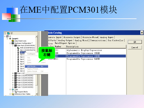
G0917006 第二次通信作业word资料15页
- 格式:doc
- 大小:61.00 KB
- 文档页数:15
本文部分内容来自网络整理,本司不为其真实性负责,如有异议或侵权请及时联系,本司将立即删除!== 本文为word格式,下载后可方便编辑和修改! ==卫星通信实验指导书篇一:卫星信号处理系统实验指导书南京工业大学卫星信号处理系统实验指导书南京莱斯大型电子系统工程有限公司201X年12月1目录实验一数字卫星接收设置................................................................... .... 3 实验二卫星信号频谱分析................................................................... .... 8 实验三直播采集源设置和信道发布 (9)2实验一数字卫星信号接收介绍一实验目的通过本实验,让学生了解数字卫星信号接收原理和数字卫星接收机包含的基本参数以及设置方法。
二实验器材数字卫星接收机,卫星地面接收天线,双极化高频头,功分器。
三实验内容说明通过现场实物讲解,让学生了解卫星信号接收和处理的过程。
四实验步骤(一)C波段卫星知识介绍卫星通信是目前国内发展重点,在许多领域中都有应用,例如,广播电视系统、电信运营、气象观测系统、应急通信系统、军事通信系统等等,学习基础卫星通信知识是很有必要的,本实验主要介绍卫星信号的接收和处理知识,本实验中卫星信号是C波段广播电视信号作为信号分析源。
C波段广播电视信号介绍如下:C波段信号的频率范围:上行频率:5925MHz-6425 MHz 下行频率:3700 MHz-4200 MHz 上行频率是指发射频率,下行频率是指接收频率。
C 波段信号上行信号分为垂直极化和水平极化; C 波段信号下行信号分为垂直极化和水平极化;极化是两种不同的传输方式;C波段常用的500 MHz带宽内,分为12个转发器进行转发,每个转发器带宽为36MHz,每个转发器中心频率间隔40 MHz,通过频率复用技术,利用正交极化方式,可以使转发器数目增加一倍。

****************************************中国联合网络通信有限公司内蒙古分公司自动路测系统技术规范书****************************************内蒙古联通移动网络公司网优中心2015年9月第一章概述1、本技术规范书(以下简称:规范书)为内蒙古联合网络通信有限公司(以下简称:甲方)向参与投标方(以下简称:乙方)提出的关于便携式室内测试设备的技术规范书。
2、此规范书中未说明,但国际、国家和行业标准已有建议的设备功能与性能的条款,卖方仪表应符合相应的最新标准与建议。
3、仪表供应厂家的质量保证体系应符合ISO9001系列的要求。
4、投标方对本招标文件的每一条款必须逐条作出明确的答复,并同时写出具体技术数据和指标,否则视该条回答无效。
技术部分中指标暂缺处应由投标方填入具体值;如有异于技术部分要求的地方,应论述其理由。
5、设备厂家应对本技术规范书的每一款做出明确答复,(‘满足’或‘不满足’,如需要可给出详细说明)否则视为废标。
6、买方有权在签订最终合同前,根据需要修改本规范书,修改后的最终文件将作为合同附件。
7、本规范书的解释权和修改权属于内蒙古联合网络通信有限公司。
第二章技术要求1.本次招标设备的范围本规范书涉及的设备为自动路测系统的前端测试设备、后台分析系统、测试软件及相关配属硬件。
招标范围如下:设备名称单位数量备注自动路测仪台158个测试模块单机版路测数据分析软件套15单机版自动路测仪操作软件套15自动路测监控分析平台套1备注:用其他方式实现单机版路测数据分析功能,也可以代替单机版路测数据分析软件。
2.现有设备情况甲方现有一套鼎利FLEET测试平台,管理全区便携式测试终端和用户感知终端的测试数据。
乙方应给出新购或者升级的详细建议以满足甲方的测试要求。
3.本次招标系统的应用范围自动道路测试系统包括前端设备和服务器平台两大部分。
前端设备应至少包含以下模块:数据采集模块、数据存储模块、数据回传模块、控制及告警模块、电源模块;服务器平台包含数据存储、数据统计与分析、语音评估、GIS等。

珠海联通短信前置机二次培训(doc 11页)前置机珠海节点网络图注:给sp接入预先分配地址:*.*.*.3----*.*.*.20/25SP增值业务介绍1.用户A定制包月的信息点播服务。
譬如:天气预报等等(包月服务最高收费不超过30/次)2.用户A 点播单次信息查询。
譬如:用户发一条信息查询现在的天气(单次服务最高收费不超过2元/次)3.用户A 向用户B 点播服务。
譬如:用户从网上给用户B发送祝福。
这时必须要进行第三方鉴权。
4.SP服务商的信息群发中国联通省内的接入号以8开头,全国通用的以9开头,例如:腾讯的QQ介入号为9777,中国移动的全国接入号以1开头。
一个接入号可以开展多项服务。
联通的165 有很多服务,如果你想使用邮件提醒功能,你只需向165 发YJ#密码就会返回邮箱的邮件和编号,邮箱的邮件和编号,YJ就是该服务业务代码。
第三方鉴权1.鉴权条件首先明确,本系统鉴权不对主叫、被叫鉴权(一般由短信中心实现),网关系统按照《sgip协议1.2版》要求,只实现对第三方付费方式的鉴权。
第三方付费:用户甲在网上(SPA)为用户乙点播短信(如生日祝福),并由用户甲付费;完成登记申请后SPA为用户乙发送祝福短信。
对此业务:发送方:SPA,接收方:用户乙,付费方:用户甲(第三方)这种情况下网关系统对付费方进行鉴权。
傲天公司网关对鉴权的判断依据:SUBMIT包中付费用户为本地、被叫用户与付费用户均为8613开头且不相等的要进行鉴权。
2.鉴权方式2.1. 鉴权要求网关系统向计费或相关部门取得第三方用户的用户信息(是否欠费),若用户欠费则系统不将该消息发送到短信中心,并由网关回复一个鉴权失败的report给消息发送方(SP);若鉴权通过,则将该短信发送给付费方所属的短信中心。
2.2. 鉴权方式一:socket通信2.2.1. 说明该方式为《sgip协议》要求方式。
2.2.2. 实现步骤1.网关判断出需要鉴权的数据包(MT);2.网关封装一个鉴权包CHECK_USER(内含付费用户号码),传输给计费或相关部门;3.计费或相关部门对付费用户进行合法性检验;4.计费或相关部门将检验结果(合法或非法)以SGIP协议包的形式(CHECKUSER_RESP)传递给网关;5.网关根据鉴权结果实现不同处理(见2.1的“鉴权要求”)。
Component Technical CommitteeATTACHMENT 6AEC - Q100-006 REV-DELECTRO-THERMALLY INDUCED PARASITIC GATE LEAKAGE TEST(GL)Component Technical CommitteeAcknowledgmentAny document involving a complex technology brings together experience and skills from many sources. The Automotive Electronics Counsel would especially like to recognize the following significant contributors to the development of this document:Mark A. Kelly Delphi Delco Electronics SystemsComponent Technical CommitteeChange NotificationThe following summary details the changes incorporated into AEC-Q100-006 Rev-D: • Sections 3.5, 3.5.1, and 3.5.2: Deleted section title 3.5, Detailed Procedure. Changed section 3.5.1 to section 3.5 and section 3.5.2 to section 3.6.Component Technical CommitteeMETHOD - 006ELECTRO-THERMALLY INDUCED PARASITICGATE LEAKAGE (GL) TESTText enhancements and differences made since the last revision of thisdocument are shown as underlined areas.1. SCOPE1.1 DescriptionThe purpose of this specification is to establish a reliable and repeatable procedure for determiningsurface mount integrated circuit susceptibility to Electro-Thermally Induced Parasitic Gate Leakage(GL). This specification may also be used as an evaluation tool for determining the susceptibility ofcircuit designs, molding compounds, fabrication processes, and post mold cure processes to GL.1.2 Reference DocumentsNot applicable.1.3 Terms and DefinitionsThe terms used in this specification are defined as follows:1.3.1 Device FailureA condition in which a device does not meet all the requirements of the acceptance criteria, asspecified in section 5, following the GL test.1.3.2 DUTAn electronic device being evaluated for its sensitivity to GL.1.3.3 Electro-Thermally Induced Parasitic Gate Leakage (GL)A trapped-charge phenomenon affecting plastic encapsulated integrated circuits in varying degreesdepending upon circuit design, fabrication technology, molding compound, and post mold cure profile.The phenomena occurs at high temperature when an electric field (E-field) is present. GL results inyield losses during high temperature processes, especially those with heated air flow (e.g., hightemperature handling and IR reflow solder operations). The phenomena can be detected as anincrease in Icc, input leakage, pin parametrics degradation, or functional failure. GL does not causepermanent damage and can be reversed by a 4 hour unbiased bake at a temperature of 125 °C (or 2hours at 150 °C).DaimlerChrysler Date Delphi Delco Electronics Systems Date Visteon Corporation DateMajdi Mortazavi Detlef Griessman Robert V. Knoell Copyright © 2003 by DaimlerChrysler, Delphi Delco Electronics Systems, and Visteon Corporation. This document may be freely reprinted with this copyright notice. This document cannot be changed without approval by the AEC Component Technical Committee.Component Technical Committee1.3.4 Electro-Thermally Induced Parasitic Gate Leakage (GL) SensitivityA GL level resulting in device failure. Sensitivity will vary depending upon the design, layout,process, and materials used.2. EQUIPMENT2.1 Test ApparatusThe apparatus required for this test consists of a GL test fixture, high voltage power supply, andthermal chamber. Figure 1 shows an equivalent test setup.Figure 1: GL Test Fixture and Set-up2.1.1 GL Test FixtureA test fixture as illustrated in Figure 1 and Appendix A. Other equivalent test fixture configurationsmay be used, but the actual fixture must meet the following requirements:1. The tungsten probe must be at a height of2.5 ± 0.5 inches above the conductive base platesurface and allow for vertical movement to facilitate voltage adjustment.2. To ensure consistent test results, all test devices must be able to be repeatably placedwith leads in contact with the conductive base plate surface by using milled recesses orequivalent markings and shall be equidistant from the high voltage tungsten probe.Component Technical Committee2.1.2 High Voltage Power SupplyA high voltage DC power supply capable of generating 20,000 volts at both positive (+) and negative(-) polarities.2.1.3 Thermal ChamberAn oven (Thermotron oven Model 51.C-B or equivalent) capable of controlled heating to atemperature of 155 °C and having adequate space to accommodate the GL test fixture.2.2 Measurement EquipmentEquipment shall include a digital voltmeter and high voltage probe to verify conformance of the GLtest fixture and resulting electric field (E-field) to the requirements of this document as specified inFigure 2, section 3.4, and Appendix A.2.2.1 Digital VoltmeterDigital voltmeter capable of accurately measuring 0 to 20,000 volts DC with a minimum sensitivity of± 1 mV.2.2.2 High Voltage ProbeHigh voltage probe capable of accurately measuring 0 to 20,000 volts DC with input resistance of1000 MΩ and ± 2% accuracy (Fluke Model 80 K-40 or equivalent).3. TEST PROCEDURE3.1 Sample SizeA total of six (6) devices shall be evaluated for GL sensitivity: a sample of three (3) devices shall bestressed at a positive (+) GL exposure and a new sample of three (3) devices shall be stressed at anegative (-) GL exposure. The use of a new sample group of three (3) devices for each GL exposurepolarity is required. Test samples must be representative of the normal process for deliverable devices;samples shall not be subjected to any additional testing or preconditioning (e.g., burn-in, etc.).Devices used for GL testing shall be discarded and shall not be retested or considered as deliverable product. GL is typically a non-destructive phenomena; however, the process of GL testing and thepost-test bake, used to verify recovery, often results in changes to the molding compound and/or lead solderability characteristics rendering the devices unsatisfactory for shipment.3.2Test TemperatureEach sample group shall be subjected to a GL exposure at 155 °C.3.3 MeasurementsPrior to GL testing, complete initial DC parametric and functional testing (initial ATE verification) shall be performed per applicable device specification. If the applicable part drawing specifies an allowable parametric shift as failure criteria, a data log of each device shall be made listing the applicableparameter measurement values (e.g., supply current, pin leakages, etc.). The data log will becompared to the parameters measured during final ATE verification to determine the failure criteria ofsection 4.Component Technical Committee3.4 GL Stress ConditionsEach sample shall be subjected to an E-field voltage potential of positive (+) or negative (-) 400 volts. A new sample of three (3) devices shall be used for each E-field voltage polarity.3.5Fixture Preparationa. Place the GL test fixture in the thermal chamber and verify both are at room temperature (seeFigure 1 and Appendix A).b Ensure the high voltage power supply is OFF and connect the positive lead to the high voltagetungsten probe. Set the height of the tungsten probe to a level of 2.5 ± 0.5 inches above theconductive base plate surface.c. Connect the negative lead of the high voltage power supply to the conductive base plate.d. Place a setup device in the fixture (located where the actual test samples will be placed) suchthat the device leads are in contact with the conductive base plate surface.e. Make sure the voltage control is set to the minimum level. Turn the high voltage power supplyto the ON position.f. Place the positive lead of the high voltage probe at the center of, and in direct contact with, thetop surface of the setup device. Connect the negative lead of the high voltage probe to theconductive base plate. The high voltage probe body should extend at a 45° ± 5° angle awayfrom the conductive base plate surface (as depicted in Figure 2). This angle is critical to themeasuring of the E-field voltage potential. As the high voltage probe body is raised (exceedingthe 45° angle requirement) or lowered (falling below the 45° angle requirement), the measuredE-field voltage potential will vary significantly.g. Monitor the setup device's E-field voltage potential using the digital voltmeter. Adjust thevoltage setting on the high voltage power supply to provide a positive (+) 400 volt E-field voltagepotential, or negative (-) 400 volt E-field voltage potential depending on the desired GLexposure, measured at the center of the setup device's top surface.h. Turn the high voltage power supply switch to the OFF position.i. Verify that the high voltage power supply is at zero (0) volts before touching the GL test fixture.j. Remove the setup device from the GL test fixture.Component Technical CommitteeFigure 2: Measurement Angle Used to Monitor E-field Voltage3.6 Detailed Test Procedurea. Ensure the high voltage power supply is OFF. Place a sample group of three (3) devices in theGL test fixture such that the device leads are in contact with the conductive base platesurface. All devices must be at the same distance from the high voltage tungsten probe as thesetup device used in section 3.5.1.b. Set the thermal chamber temperature to 155 °C. The use of a thermocouple placed in directcontact with the GL test fixture conductive base plate surface may be used to monitor thetemperature of the sample group devices.c. Verify the test sample devices are at the specified temperature. Allow the test fixture andsample group of three (3) devices to stabilize at the specified temperature for 15 minutes.d. Turn the high voltage power supply switch to the ON position.e. Allow the devices and GL test fixture (with the E Field voltage applied) to soak for a 2 minutedwell time as indicated in Figure 3.f. After 2 minutes of the total dwell time have elapsed, begin reducing the thermal chambertemperature to 100 °C or less with the E-field voltage still applied. This can beaccomplished by opening the thermal chamber door while the circulating fans are operating.Thermal chamber heating and cooling times will vary and a longer ramp-down time may berequired when reducing the thermal chamber temperature. The total ramp-down time (155°C to 100 °C) shall not exceed 10 minutes (see Figure 3).Component Technical Committeeg. Once the sample group of three (3) devices reaches a temperature of 100 °C, turn the highvoltage power supply switch to the OFF position. A thermocouple placed in direct contactwith the GL test fixture conductive base plate surface may be used to monitor thetemperature of the sample group devices.h. Verify the high voltage power supply is at zero (0) volts before touching the GL test fixture.i. After cooling to room temperature, remove the sample group of three (3) devices from the GLtest fixture.j. Submit the devices for complete DC parametric and functional testing (final ATE verification) per applicable device specification within 96 hours of GL exposure and determine whether the devices meets the acceptance criteria requirements specified in section 5. The storagetemperature between GL exposure and final ATE verification shall not exceed 30 °C.k. Subject all failing devices to an unbiased bake of 4 hours at a temperature of 125 °C (or 2 hours at 150 °C) and then submit for complete DC parametric and functional testing (ATE re-verification). GL failures will always recover when subjected to a 4 hour unbiased bake at 125 °C (or 2 hours at 150 °C). If the failing devices do not recover following the unbiased bake,then the devices may have been damaged (due to handling, EOS, ESD, etc.). Failing devices that do not recover shall be eliminated from the GL data.l. Record pass/fail and any other pertinent observations for each device.m. Reverse the high voltage power supply polarity, verify the E-field voltage potential (as specified in section 3.5.1), and repeat steps (a) through (l) above using a new sample group of three (3) devices.Figure 3: Dwell Time and Ramp-Down Time for GL TestComponent Technical Committee4. FAILURE CRITERIAA device will be defined as a failure if, after exposure to GL, the device fails any of the following criteria:1. The device exceeds the allowable shift value. Specific parameters and allowable shift valuesshall be as defined in the applicable device specification. During initial ATE verification, a datalog shall be made for each device listing the applicable parameter measurement values. Thedata log will be compared to the parameters measured during final ATE verification todetermine the shift value. Devices exceeding the allowable shift value will be defined as afailure.2. The device no longer meets the device specification requirements. Complete DC parametricand functional testing shall be performed per applicable device specification.5. ACCEPTANCE CRITERIAA device passes a GL exposure level if all devices in the sample group stressed at that GL level pass.All the devices and sample groups used must pass the measurement requirements specified in section3 and the failure criteria requirements specified in section4 following both positive (+) and negative (-)400 volt E-field exposures in order for the devices to be considered acceptable.Component Technical CommitteeAppendix A(suggested GL test fixture)This appendix provides suggested general construction features of the GL test fixture. Other equivalent test fixture configurations may be used, but the actual fixture must meet the requirements of section 2.1.1. The dimensions shown are approximate and are not critical to the test fixture construction. Figures A1 through A5 illustrate the GL test fixture assembly and major components.Note:Attach High VoltageWarning Label totest fixtureFigure A1: GL Test Fixture AssemblyComponent Technical CommitteeFigure A2: Conductive Base PlateThe base plate is constructed from electrically conductive material (e.g., .125 - .250 inch aluminum stock). The plate is approximately 6 inches square and serves to support and locate the devices under test and as one pole of the test voltage. Milled recesses may be used for repeatable device placement during GL testing (see Figures A1 and A2). The suggested recesses may be milled directly into the plate to ensure consistent device placement and orientation with respect to the tungsten probe center-line. The recesses, large enough to accommodate the largest device to be tested, are located 120 degrees apart and equidistant from the center of the base plate. The absolute distance from center (approximately one inch) is not critical.The lower left hand corner (dashed line section) is cut off on a diagonal to facilitate device handling and to reduce thermal mass. A lower post section, or leg, is added to the diagonal side for stability (see FigureA1).Note: The aluminum plate should be alodine coated for protection against corrosion and to retain electrical quality.Component Technical CommitteeFigure A3: Top Insulating PlateThe top insulating plate serves to support and locate the tungsten probe at the center of the GL test fixture. It establishes and maintains the probe to device distance during set-up and test. The top plate is fabricated from a triangular piece of .250 inch Teflon, Delrin, or other insulating material which is capable of withstanding an environment of 200 °C and ± 20,000 volts.A .049 inch diameter hole, used to position the tungsten probe, is centered on the diagonal side so as to be directly above the base plate center point after assembly. Clearance holes are drilled at each corner for assembly screws.Component Technical Committee60 degreeradius.049 "approximately 4 "Figure A4: Tungsten ProbeGrind a 60 degree point on a 4 inch length of 0.049 inch diameter tungsten wire (or a diameter of tungsten wire that is readily available; the diameter of the wire is not critical). This will provide an E-field potential at the specified test voltage, as measured on the top surface of the device approximately 2 inches from the tungsten probe point.Figure A5: Tungsten Probe Clamping MechanismComponent Technical CommitteeRevision HistoryRev #-A B C D Date of changeJune 9, 1994May 15, 1995Sept. 6, 1996Oct. 8, 1998July 18, 2003Brief summary listing affected sectionsInitial ReleaseAdded Copyright statement. Revised the following: Foreword; Sections2.1.2,3.1, 3.2.2 (d, f, and g), and 3.2.3 (a, b, c, f, g, and l); Figures 1, 2,and 3; Appendix A.Deleted old Sections 1.3.3, 1.3.4, 1.3.5, 1.3.6, 1.3.7, 2.1.1, 3.1, 3.2.1, 3.3,3.4, 3.5, and 3.6. Added new Sections 1.3.1, 1.3.4, 2.2, 2.2.1, 2.2.2, 3.1,3.2, 3.3, 3.4, and 5.0. Revised the following: Sections 1.1, 1.3, 1.3.2, 1.3.3,2.1, 2.1.1, 2.1.2,3.5.1 (a, e, f, g, h, and i), 3.5.2 (a, b, c, e, f, g, h, i, j, k, l,and m), 4.0, and Appendix A; Figures 1, 2, 3, A1, and A2.Revised the following: Sections 3.4, 3.5.1 (g), 5; Figure 1. Revisions reflecta change in E-field requirement from ±700 volt to ±400 volt.Revised the following: Sections 3.5, 3.5.1, and 3.5.2.。
西安电子科技大学现代通信系统测量实验课程实验报告实验名称无线通信系统误码率测量通信工程学院1701017班成绩姓名方骏驰学号17010170007同作者07号实验日期2020年10月13日指导教师评语:指导教师:年月日实验报告内容基本要求及参考格式一、实验目的二、实验所用仪器(或实验环境)三、实验基本原理及步骤(或方案设计及理论计算)四、实验数据记录(或仿真及软件设计)五、实验结果分析及回答问题(或测试环境及测试结果)六、写出自己实验心得体会一.实验目的1.了解不同编码的编码原理以及其编码特性2.比较不同数据速率,不同编码方式下无线通信系统的性能3.掌握误码仪的使用方法,使用外时钟正确测量通信系统的误码率二.实验原理1.信源编码①pn序列②16比特序列2.信道编码①汉明编码②卷积编码③循环编码④交织编码3.误码仪的使用及原理(一)信源编码1.①pn序列2.pn序列是一种伪噪声序列,这类序列具有类似随机噪声的一些统计特性,但和真正的随机信号不同,它可以重复产生和处理,故称作伪随机噪声序列。
2.在二进制移位寄存器中,若n为移位寄存器的级数,n级移位寄存器共有2n个状态,除去全0状态外还剩下2n-1中状态,因此它能产生的最大长度的码序列为2n-1位,也就是说,一个n级线性反馈移位寄存器产生的最长周期等于2n-1寄存器的状态决定于时钟控制下输入的信息(“0”或“1”),例如第I级移位寄存器状态决定于前一时钟脉冲后的第i-1级移位寄存器的状态。
图中C0,C1,…,Cn均为反馈线,其中C0=C1=1,表示反馈连接。
因为m序列是由循环序列发生器产生的,因此C0和Cn肯定为1,即参与反馈。
而反馈系数C1,C2,…,Cn-1,若为1,参与反馈;若为0,则表示断开反馈线,即开路,无反馈连线。
图中Ci表示反馈线的两种可能连接方式,Ci=1表示连线接通,第n-i级输出加入反馈中;Ci=0表示连线断开,第n-i级输出未参加反馈。
信息通信建设工程预算定额第二册有线通信设备安装工程(修订送审稿)中华人民共和国工业和信息化部2目录总说明................................................................................................................................................................. a 册说明................................................................................................................................................................. e 第一章安装机架、缆线及辅助设备 . (1)说明 (1)第一节安装机架(柜)、机箱 (2)第二节安装配线架 (5)一、安装总配线架 (5)二、安装数字分配架、光分配架 (7)第三节安装保安配线箱 (8)第四节安装列架照明、机台照明、机房信号灯盘 (9)第五节布放设备缆线、软光纤 (10)一、布放线缆承载设施 (10)二、布放设备电缆 (11)三、布放设备导线 (14)四、布放软光纤 (16)五、布放电力电缆 (18)1第二章安装、调测光纤数字传输设备 (22)说明 (22)第一节安装测试传输设备 (24)第二节安装测试波分复用设备、光传送网设备 (28)第三节安装、调测再生中继及远供电源设备 (35)第四节安装、调测网络管理系统设备 (36)第五节调测系统通道 (37)一、调测传输设备系统通道 (37)二、调测波分复用设备、光传送设备系统通道 (38)三、网络保护及光路优化 (39)四、调测系统通道中间站配合、光纤复测等 (40)第六节安装、调测同步网设备 (41)第七节安装、调测无源光网络设备 (42)一、安装测试光线路终端(OLT)设备 (42)二、安装测试光网络单元(ONU)/光网络终端(ONT)设备 (43)三、安装调测网管系统、接入网功能验证及性能测试 (44)第三章安装、调测数据通信设备 (46)说明 (46)2一、安装、调测数字数据网设备 (47)二、安装、调测宽带接入设备 (49)三、安装、调测路由器设备 (50)四、安装、调测交换机设备 (52)五、安装、调测服务器设备 (53)六、安装、调测局域网终端及附属设备 (54)第二节安装、调试数据存储设备 (56)第三节安装、调试网络安全设备 (58)第四章安装、调测交换设备 (59)说明 (59)第一节安装、调测交换设备 (60)一、安装交换设备硬件 (60)二、调测交换设备 (61)第二节安装、调测操作维护中心设备 (65)第三节调测智能网设备 (66)第四节安装、调测信令网设备 (67)第五章安装、调测视频监控设备 (68)说明 (68)3第二节布放线缆 (71)第三节安装调测摄像设备 (72)第四节安装调测光端设备 (73)第五节安装辅助设备 (74)第六节安装调测视频控制设备 (75)第七节安装编解码设备 (76)第八节安装音频、视频、脉冲分配器 (77)第九节安装报警设备 (78)第十节安装显示设备 (79)第十一节系统调测 (80)4总说明一、《信息通信建设工程预算定额》(以下简称“预算定额”)是完成规定计量单位工程所需要的人工、材料、施工机械和仪表的消耗量标准。
数据通信与网络作业姓名:学号:CH9Q14. 当我们打越洋电话的时,有时会感到延迟,能说明其原因吗?答:电话网络是由多级交换局(本地局、中继局、地区局)组成的。
在美国,将整个国家划分为200多个本地接入和传送区域(LATA),在一个LATA 内部提供服务的运营商称为本地交换电信公司(LEC),在一个LATA内部交换局中,只有本地局与中继局,当需要跨LATA进行通信的时候,就需要跨区交换电信公司(IXC)提供LATA之间的通信服务。
中国的通信运营商提供的固话通信服务过程与此类似。
通过上面的介绍,我们可知,一次越洋通信的过程如下:呼叫方接通本地局,本地局接入LATA内部的中继局,中继局通过服务接入点(POP)接入IXC网络,数据在IXC网络内部通过海底电缆进行传输,到达大洋彼岸后,通过POP接入该地区LATA内部的中继局,然后接入中继局内部的本地局,最后接通被呼叫方。
可见,一次越洋通话,中间会经过6次通信转接,而在每次通信转接中,程控机进行交换时总是会出现程序延迟。
同时,在发送方进行的模数转换与接收方进行的数模转换同样会使通话产生延迟,这样,我们就不可避免的会在越洋电话中感觉到延时。
Q17. 使用下列技术计算,下载1000000字节所需要的最小时间?a. V32 modemb. V32bis modemc. V90 modem答:d=1000kB=8000kb,t=传输时间,v=传输速度 t=d/va. V32 modem v=9.6kbps,t=8000kb/9.6kbps≈833sb.V32bis modem v=14.4kbps,t=8000kb/14.4kbps≈556sc. V90 modem v=33.6kbps,t=8000kb/56kbps≈143sCH10Q13. 按表10.1,发送方发送数据字10。
一个3位突发性差错损坏了码字,接收方能否检测出差错?说出理由。
答:由表10.1我们可知,dataword=10时,codeword=101,一个3位突发性差错将改变所有的该codeword的所有位,所以接收方收到的codeword=010,接收方查询后发现为无效codeword,丢弃该codeword。
综上所述,接收方是可以检错的。
Q14. I按表10.2,发送方发送数据字10。
如果一个3位突发性差错损坏了码字的前3位,接收方能否检测出差错?说明理由。
答:由表10.2我们可知,dataword=10时,codeword=10101,一个3为突发性差错改变codeword前三位以后,接收方收到的codeword=01001,接收方查询后发现为无效codeword,丢弃该codeword。
综上所述,接收方是可以检错的。
CH11Q9. 比较和对比回退N帧ARQ协议和选择性重复ARQ协议。
答:1.回退N帧ARQ协议:发送窗口大于1,接收窗口等于1。
发送方可以连续的发送帧,但一旦待确认的帧错误或定时器到时,将重发所有待确认的帧。
2.选择性重复ARQ协议:发送窗口大于1,接收窗口也大于1。
双方只重传错误的或超时的帧,并且发送方保留后续帧的副本。
选择性重复ARQ协议与回退N帧ARQ协议相比,减少了重传出错帧以后所有正确帧的开销,但是接收方的算法也相应的复杂化了Q17. 一个发送方发送一系列分组到同一个目的地,使用一个5位长度的序列。
如果序列号以0开始,发送一百个分组后序号是多少?答:因为序列号长度为5,所以序号为0~31,发送100个分组后,序号为3。
Q23. 为使用捎带选择性等待ARQ设计一个双向算法。
注意双方都使用同一个算法。
答:if (Frame Type is Data){if (corrupted (Frame)) AND (NOT NakSent)endNAK (Rn);NakSent = true;Sleep();if (ackNo between Sf and Sn)while (Sf < ackNo){ Purge (Sf);StopTimer (Sf);Sf = Sf + 1;if ((seqNo <> Rn) AND (NOT NakSent)){ SendNAK (Rn); NakSent = true; }if ((seqNo in window) AND (NOT Marked (seqNo))StoreFrame (seqNo);Marked (seqNo) = true;while (Marked (Rn))DeliverData (Rn);Purge (Rn);Rn = Rn + 1;AckNeeded = true;} // End if (Frame Type is Data) }// End if (arrival event) if (Event (TimeOut (t)))// The timer expires { StartTimer (t); SendFrame (t); } }// End Repeat foreverCH12Q10. 我们使用有线电视的通道访问因特网时,需要一个多路访问协议吗?为什么?答:我们可知,CATV信号传输过程中,通常使用同轴电缆,且传输方式应该是FDM,而且,一条电缆在访问internet时通常是多用户使用的,所以应该使用多路访问技术,根据数模转换的性质与信号传输介质的限制,通常使用的多路访问技术应该是FDMA与TDMA。
Q15. 在数据速率为10Mbps的CSMA/CD网络中,为了冲突检测过程的正确操作,最小帧长度是512比特,如果我们把数据速率提高到100M,那么最小帧长度应该是多少?那么提高到1Gbps、10Gbps分别是多少呢?答:在10Mbps中,最小帧长度为512bits,所以,帧的传输时间为10Mbps/512bits≈51.2us。
当数据传输率为100Mbps时,帧的最小长度应该为100Mbps*51.2us=5120bits=5Kbits;当数据传输率为1Gbps时,帧的最小长度应该为1Gbps*51.2us=51200bits=50Kbits;当数据传输率为10Gbps时,帧的最小长度应该为10Gbps*51.2us=512000bits=500Kbits。
Q26. 你能解释为什么ALOHA中的脆弱时间依靠Tfr ,而CSMA中依靠 Tp?答:在ALOHA协议中,一个站点若想成功的发送帧,那么,在帧发送期间,必须没有站点在发送帧,所以,这个协议的脆弱时间只能与帧传输时间相关。
在纯ALOHA协议中,脆弱时间等于两倍的帧传输时间;而在时隙ALOHA 协议中,脆弱时间等于帧传输时间。
在CSMA协议中,一个站点若想成功的发送帧,那么,在帧发送期间,必须保证其他所有站点能侦听到这个帧信号,所以,这个协议的脆弱时间只能与最大传输时间有关。
CH13Q5. 交换机和网桥之间的关系是什么?答:二层交换机与网桥工作在同一层。
在一个有M台机器的网络中,一个有N个端口的网桥将整个网络分割为N个冲突域,每个冲突域中的机器共享带宽;而一个M口的交换机将整个网络分为M个冲突域,也就是每台机器独享带宽,这样看来,交换机网络比网桥网络的传输速度要快得多,交换机就是一个密集端口的网桥,同时,交换机相比网桥来说,还具有快速处理分组的附加功能。
Q17. 一个以太网MAC子层从上层接收1510个字节的数据。
这些字节能压缩在一个帧内吗?如果不可以的话,那么要发送多少帧?每个帧中的数据大小是多少?答:因为MAC帧的数据长度最大为1500字节,所以,必须要发送两个MAC 帧。
第一个帧长度为1518字节,数据大小为1500字节;第二个帧长度为64字节,数据大小为46字节,包括剩余的10字节数据与填充的36字节数据。
CH14Q4. 无线LAN使用的访问方式是什么?答:无线Lan使用的访问方式是CSMA/CA。
Q5. NAV的目的是什么?答:NAV的目的在于当介质被占用的情况下,控制站点推迟发送数据的时间。
当信道被占用时,待发送站点根据收到的正发送站点的RTS帧中包含的占用时间,启动NAV定时器,该定时器表示在允许检查信道是否空闲之前还需等待多长时间。
CH15Q17. 在图15.6中,我们使用一个网桥。
我们能用路由器代替网桥吗?请解释原因。
答:我们可以用路由器代替网桥。
网桥在这里的作用起转发和连接不同网段的作用。
路由器也是具有转发和连接不同网段的功能,可以承担这样的作用。
网桥和路由器不同的是转发的依据不同,网桥依据MAC地址,路由器依据IP地址。
Q18. 网桥使用过滤表,路由使用路由表。
你能解释差别吗?答:网桥将两个相似的网络连接起来,并对网络数据的流通进行管理。
它工作于数据链路层,不但能扩展网络的距离或范围,而且可提高网络的性能、可靠性和安全性。
网络1和网络2通过网桥连接后,网桥接收网络1发送的数据包,使用过滤表检查帧包含的MAC地址,如果地址属于网络1,它就将其放弃,相反,如果是网络2的地址,它就继续发送给网络2.这样可利用网桥隔离信息,将网络划分成多个网段,隔离出安全网段,防止其他网段内的用户非法访问。
路由器属于OSI第三层即网络层设备,它根据IP地址进行寻址,是基于分组的逻辑地址路由分组,通过路由表路由协议产生,路由表供路由选择时使用,表中包含的信息决定了数据转发的策略。
打个比方,路由表就像我们平时使用的地图一样,标识着各种路线,路由表中保存着子网的标志信息、网上路由器的个数和下一个路由器的名字等内容。
路由表通常是动态的,使用路由协议更新。
可以由路由器自动调整,也可以由主机控制。
CH16Q10. GEO卫星有几种轨道?解释你的答案。
答:因为GEO卫星的移动速度必须与地球的自转速度保持一致,这样才可称之为同步卫星,所以只有一种轨道,即赤道平面轨道,高度距地球大约22K英里。
Q15. 铱星系统和全球星系统的主要区别是什么?答:铱星系统和全球星系统都是一种近地轨道卫星系统。
两者之间主要的区别在于中继系统。
在铱星系统中,两个远距离用户之间的通信需要在几颗卫星之间传递,而全球星系统的通信不但需要卫星,也需要地面站,这意味着地面站可以产生能量更高的信号。
CH19Q26. 某一ISP被指派以150.80.0.0/16为起始地址的块,该ISP想要按下列规则给2600个客户分配块:A.第一组是200个中型的企业,每一个需要128个地址;B.第二组是400个小型的企业,每一个需要16个地址;c.第三组是2000个家庭用户,每一个需要4个地址。
设计这些子块并对每一个子块用斜杠标记法表示。
求这些块分配后还有多少可能地址?答:由题意某一ISP共有IP地址数为232-16=65536个地址,ISP需要按如下给3组客户分发这些地址。