
MAX4081TAUA中文资料
- 格式:pdf
- 大小:366.02 KB
- 文档页数:15
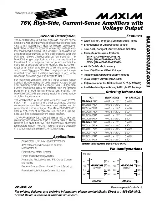

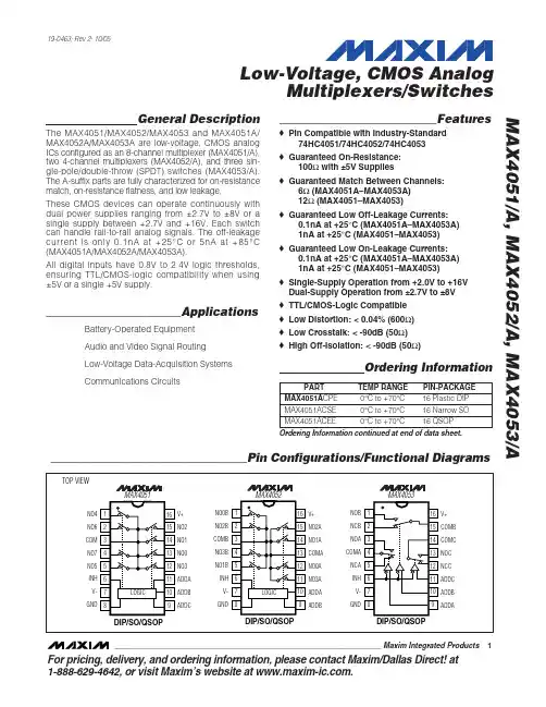
General DescriptionThe MAX4051/MAX4052/MAX4053 and MAX4051A/MAX4052A/MAX4053A are low-voltage, CMOS analog ICs configured as an 8-channel multiplexer (MAX4051/A),two 4-channel multiplexers (MAX4052/A), and three sin-gle-pole/double-throw (SPDT) switches (MAX4053/A).The A-suffix parts are fully characterized for on-resistance match, on-resistance flatness, and low leakage.These CMOS devices can operate continuously with dual power supplies ranging from ±2.7V to ±8V or a single supply between +2.7V and +16V. Each switch can handle rail-to-rail analog signals. The off-leakage current is only 0.1nA at +25°C or 5nA at +85°C (MAX4051A/MAX4052A/MAX4053A).All digital inputs have 0.8V to 2.4V logic thresholds,ensuring TTL/CMOS-logic compatibility when using ±5V or a single +5V supply.________________________ApplicationsBattery-Operated Equipment Audio and Video Signal Routing Low-Voltage Data-Acquisition Systems Communications Circuits____________________________Features♦Pin Compatible with Industry-Standard74HC4051/74HC4052/74HC4053♦Guaranteed On-Resistance:100Ωwith ±5V Supplies♦Guaranteed Match Between Channels:6Ω(MAX4051A–MAX4053A)12Ω(MAX4051–MAX4053)♦Guaranteed Low Off-Leakage Currents:0.1nA at +25°C (MAX4051A–MAX4053A)1nA at +25°C (MAX4051–MAX4053)♦Guaranteed Low On-Leakage Currents:0.1nA at +25°C (MAX4051A–MAX4053A)1nA at +25°C (MAX4051–MAX4053)♦Single-Supply Operation from +2.0V to +16V Dual-Supply Operation from ±2.7V to ±8V ♦TTL/CMOS-Logic Compatible ♦Low Distortion: < 0.04% (600Ω)♦Low Crosstalk: < -90dB (50Ω)♦High Off-Isolation: < -90dB (50Ω)MAX4051/A, MAX4052/A, MAX4053/ALow-Voltage, CMOS AnalogMultiplexers/Switches________________________________________________________________Maxim Integrated Products1___________________________________Pin Configurations/Functional Diagrams19-0463; Rev 2; 10/05Ordering Information continued at end of data sheet.For pricing, delivery, and ordering information,please contact Maxim/Dallas Direct!at 1-888-629-4642, or visit Maxim’s website at .M A X 4051/A , M A X 4052/A , M A X 4053/ALow-Voltage, CMOS Analog Multiplexers/Switches 2_______________________________________________________________________________________ABSOLUTE MAXIMUM RATINGSELECTRICAL CHARACTERISTICS—Dual Supplies(V+ = +4.5V to +5.5V, V- = -4.5V to -5.5V, T A = T MIN to T MAX , unless otherwise noted. Typical values are at T A = +25°C.)Stresses beyond those listed under “Absolute Maximum Ratings” may cause permanent damage to the device. These are stress ratings only, and functional operation of the device at these or any other conditions beyond those indicated in the operational sections of the specifications is not implied. Exposure to absolute maximum rating conditions for extended periods may affect device reliability.Voltages Referenced to GNDV+........................................................................-0.3V to +17V V-..........................................................................+0.3V to -17V V+ to V-................................................................-0.3V to +17V Voltage into Any Terminal (Note 1)..........(V- - 2V) to (V+ + 2V)or 30mA (whichever occurs first)Continuous Current into Any Terminal..............................±30mA Peak Current, NO or COM(pulsed at 1ms, 10% duty cycle).................................±100mAContinuous Power Dissipation (T A = +70°C)Plastic DIP (derate 10.53mW/°C above +70°C)............842mW Narrow SO (derate 8.70mW/°C above +70°C)..............696mW QSOP (derate 8.00mW/°C above +70°C).....................640mW CERDIP (derate 10.00mW/°C above +70°C)................800mW Operating Temperature RangesMAX405_C_ E/MAX405_AC_E.............................0°C to +70°C MAX405_E_ E/MAX405_AE_E...........................-40°C to +85°C MAX405_MJE/MAX405_AMJE........................-55°C to +125°C Storage Temperature Range.............................-65°C to +150°C Lead Temperature (soldering, 10s).................................+300°CNote 1:Signals on any terminal exceeding V+ or V- are clamped by internal diodes. Limit forward-diode current to maximumcurrent rating.ELECTRICAL CHARACTERISTICS—Dual Supplies (continued)MAX4051/A, MAX4052/A, MAX4053/A Low-Voltage, CMOS Analog Multiplexers/Switches(V+ = +4.5V to +5.5V, V- = -4.5V to -5.5V, T A= T MIN to T MAX, unless otherwise noted. Typical values are at T A= +25°C.)M A X 4051/A , M A X 4052/A , M A X 4053/ALow-Voltage, CMOS Analog Multiplexers/Switches 4_______________________________________________________________________________________Note 2:The algebraic convention is used in this data sheet; the most negative value is shown in the minimum column.Note 3:∆R ON = R ON(MAX)- R ON(MIN).Note 4:Flatness is defined as the difference between the maximum and minimum value of on-resistance as measured over thespecified analog signal ranges; i.e., V NO = 3V to 0V and 0V to -3V.Note 5:Leakage parameters are 100% tested at maximum-rated hot operating temperature, and guaranteed by correlation atT A = +25°C.Note 6:Guaranteed by design, not production tested.ELECTRICAL CHARACTERISTICS—Dual Supplies (continued)(V+ = +4.5V to +5.5V, V- = -4.5V to -5.5V, T A = T MIN to T MAX , unless otherwise noted. Typical values are at T A = +25°C.)ELECTRICAL CHARACTERISTICS—Single +5V SupplyMAX4051/A, MAX4052/A, MAX4053/A Low-Voltage, CMOS Analog Multiplexers/Switches(V+ = +4.5V to +5.5V, V- = 0V, T A= T MIN to T MAX, unless otherwise noted. Typical values are at T A= +25°C.)M A X 4051/A , M A X 4052/A , M A X 4053/ALow-Voltage, CMOS Analog Multiplexers/Switches 6_______________________________________________________________________________________ELECTRICAL CHARACTERISTICS—Single +5V Supply (continued)(V+ = +4.5V to +5.5V, V- = 0V, T A = T MIN to T MAX , unless otherwise noted. Typical values are at T A = +25°C.)Note 2:The algebraic convention is used in this data sheet; the most negative value is shown in the minimum column.Note 3:∆R ON = R ON(MAX)- R ON(MIN).Note 4:Flatness is defined as the difference between the maximum and minimum value of on-resistance as measured over thespecified analog signal ranges; i.e., V NO = 3V to 0V and 0V to -3V.Note 5:Leakage parameters are 100% tested at maximum-rated hot operating temperature, and guaranteed by correlation atT A = +25°C.Note 6:Guaranteed by design, not production tested.ELECTRICAL CHARACTERISTICS—Single +3V SupplyMAX4051/A, MAX4052/A, MAX4053/A Low-Voltage, CMOS Analog Multiplexers/Switches(V+ = +3.0V to +3.6V, V- = 0V, T A= T MIN to T MAX, unless otherwise noted. Typical values are at T A= +25°C.)M A X 4051/A , M A X 4052/A , M A X 4053/ALow-Voltage, CMOS Analog Multiplexers/Switches 8_______________________________________________________________________________________ELECTRICAL CHARACTERISTICS—Single +3V Supply (continued)(V+ = +3.0V to +3.6V, V- = 0V, T A = T MIN to T MAX , unless otherwise noted. Typical values are at T A = +25°C.)Note 2:The algebraic convention is used in this data sheet; the most negative value is shown in the minimum column.Note 3:∆R ON = R ON(MAX)- R ON(MIN).Note 4:Flatness is defined as the difference between the maximum and minimum value of on-resistance as measured over thespecified analog signal ranges; i.e., V NO = 3V to 0V and 0V to -3V.Note 5:Leakage parameters are 100% tested at maximum-rated hot operating temperature, and guaranteed by correlation atT A = +25°C.Note 6:Guaranteed by design, not production tested.MAX4051/A, MAX4052/A, MAX4053/ALow-Voltage, CMOS AnalogMultiplexers/Switches_______________________________________________________________________________________911030-5-31ON-RESISTANCE vs. V COM(DUAL SUPPLIES)5090V COM (V)R O N (Ω)-13701004080605-40-22411030-5-31ON-RESISTANCE vs. V COMAND TEMPERATURE (DUAL SUPPLIES)5090V COM (V)R O N (Ω)-137********605-40-2243005002ON-RESISTANCE vs. V COM(SINGLE SUPPLY)100200V COM (V)R O N (Ω)41502502752257517512515318002ON-RESISTANCE vs. V COMAND TEMPERATURE (SINGLE SUPPLY)100V COM (V)R O N (Ω)4601401601208040153-5-31CHARGE INJECTION vs. V COM-55V COM (V)Q j (p C )-135-40-2240.1OFF-LEAKAGE vs.TEMPERATURE1000TEMPERATURE (°C)O F F -L E A K A G E (p A )101100-5012525-25075501000.1ON-LEAKAGE vs.TEMPERATURE100010,000TEMPERATURE (°C)O N -L E A K A G E (p A )101100-5012525-25075501000.1SUPPLY CURRENT vs.TEMPERATURE10TEMPERATURE (°C)I +, I - (n A )1-5012525-2507550100__________________________________________Typical Operating Characteristics(V+ = +5V, V- = -5V, GND = 0V, T A = +25°C, unless otherwise noted.)M A X 4051/A , M A X 4052/A , M A X 4053/ALow-Voltage, CMOS Analog Multiplexers/Switches 10__________________________________________________________________________________________________________________Typical Operating Characteristics (continued)(V+ = +5V, V- = -5V, GND = 0V, T A = +25°C, unless otherwise noted.)_____________________________________________________________Pin Descriptions67————31, 2, 4, 5——Note:NO, NC, and COM pins are identical and interchangeable. Any may be considered an input or output; signals pass equallywell in both directions.67123515NO0B–NO3B ———MAX4052/MAX4052AMAX4053/MAX4053A0.01101001k10kTOTAL HARMONIC DISTORTIONvs. FREQUENCY0.1FREQUENCY (Hz)T H D (%)110100PIN0-10-900.010.1110100300FREQUENCY RESPONSE-80-70FREQUENCY (MHz)L O S S (d B )P H A S E (D E G R E E S )-50-60-40-20-3050-40-35-30-20-25-15-5-10INSERTION LOSS50Ω IN/OUT OFF-ISOLATIONON PHASE__________Applications InformationPower-Supply ConsiderationsOverviewThe MAX4051/MAX4052/MAX4053 and MAX4051A/MAX4052A/MAX4053A construction is typical of most CMOS analog switches. They have three supply pins:V+, V-, and GND. V+ and V- are used to drive the inter-nal CMOS switches and set the limits of the analog volt-age on any switch. Reverse ESD-protection diodes are internally connected between each analog signal pin and both V+ and V-. If any analog signal exceeds V+ or V-, one of these diodes will conduct. During normal operation, these (and other) reverse-biased ESD diodes leak, forming the only current drawn from V+ or V-.Virtually all the analog leakage current comes from the ESD diodes. Although the ESD diodes on a given signal pin are identical, and therefore fairly well balanced,they are reverse biased differently. Each is biased by either V+ or V- and the analog signal. This means their leakages will vary as the signal varies. The difference in the two diode leakages to the V+ and V- pins consti-tutes the analog signal path leakage current. All analog leakage current flows between each pin and one of the supply terminals, not to the other switch terminal. This is why both sides of a given switch can show leakage cur-rents of either the same or opposite polarity.There is no connection between the analog signal paths and GND.MAX4051/A, MAX4052/A, MAX4053/AMultiplexers/Switches______________________________________________________________________________________11Table 1. Truth Table/Switch ProgrammingX = Don’t care * ADDC not present on MAX4052.Note:NO and COM pins are identical and interchangeable. Either may be considered an input or output; signals pass equally wellin either direction.M A X 4051/A , M A X 4052/A , M A X 4053/AV+ and G ND power the internal logic and logic-level translators, and set both the input and output logic lim-its. The logic-level translators convert the logic levels into switched V+ and V- signals to drive the gates of the analog signals. This drive signal is the only connec-tion between the logic supplies (and signals) and the analog supplies. V+ and V- have ESD-protection diodes to GND.The logic-level thresholds are TTL/CMOS compatible when V+ is +5V. As V+ rises, the threshold increases slightly, so when V+ reaches +12V, the threshold is about 3.1V; above the TTL-guaranteed high-level mini-mum of 2.8V, but still compatible with CMOS outputs.Bipolar SuppliesThese devices operate with bipolar supplies between ±3.0V and ±8V. The V+ and V- supplies need not be symmetrical, but their sum cannot exceed the absolute maximum rating of +17V.Single SupplyThese devices operate from a single supply between +3V and +16V when V- is connected to GND. All of the bipolar precautions must be observed. At room temper-ature, they actually “work” with a single supply at near or below +1.7V, although as supply voltage decreases,switch on-resistance and switching times become very high.Overvoltage ProtectionProper power-supply sequencing is recommended for all CMOS devices. Do not exceed the absolute maxi-mum ratings, because stresses beyond the listed rat-ings can cause permanent damage to the devices.Always sequence V+ on first, then V-, followed by the logic inputs (NO) and by COM. If power-supply sequencing is not possible, add two small signal diodes (D1, D2) in series with the supply pins for overvoltage protection (Figure 1).Adding diodes reduces the analog signal range to one diode drop below V+ and one diode drop above V-, but does not affect the devices’ low switch resistance and low leakage characteristics. Device operation is unchanged, and the difference between V+ and V-should not exceed 17V. These protection diodes are not recommended when using a single supply if signal levels must extend to ground.High-Frequency PerformanceIn 50Ωsystems, signal response is reasonably flat up to 50MHz (see Typical Operating Characteristics ).Above 20MHz, the on response has several minor peaks which are highly layout dependent. The problem is not turning the switch on, but turning it off. The off-state switch acts like a capacitor, and passes higher frequencies with less attenuation. At 10MHz, off isola-tion is about -45dB in 50Ωsystems, becoming worse (approximately 20dB per decade) as frequency increases. Higher circuit impedances also make off iso-lation worse. Adjacent channel attenuation is about 3dB above that of a bare IC socket, and is entirely due to capacitive coupling.Multiplexers/Switches 12______________________________________________________________________________________Figure 1. Overvoltage Protection Using External Blocking DiodesMAX4051/A, MAX4052/A, MAX4053/AMultiplexers/Switches______________________________________________________________________________________13Figure 2. Address Transition Time______________________________________________Test Circuits/Timing DiagramsFigure 3. Enable Switching TimeM A X 4051/A , M A X 4052/A , M A X 4053/AMultiplexers/Switches 14______________________________________________________________________________________MAX4051/A, MAX4052/A, MAX4053/AMultiplexers/Switches______________________________________________________________________________________15Figure 4. Break-Before-Make IntervalFigure 5. Charge InjectionM A X 4051/A , M A X 4052/A , M A X 4053/AMultiplexers/Switches 16______________________________________________________________________________________Figure 6. Off-Isolation, On-Loss, and CrosstalkFigure 7. NO/COM CapacitanceMAX4051/A, MAX4052/A, MAX4053/AMultiplexers/Switches______________________________________________________________________________________17Chip InformationTRANSISTOR COUNT: 161SUBSTRATE CONNECTED TO V+.___________________________________________Ordering Information (continued)M A X 4051/A , M A X 4052/A , M A X 4053/AMultiplexers/SwitchesPackage Information(The package drawing(s) in this data sheet may not reflect the most current specifications. For the latest package outline information,go to /packages .)Maxim cannot assume responsibility for use of any circuitry other than circuitry entirely embodied in a Maxim product. No circuit patent licenses are implied. Maxim reserves the right to change the circuitry and specifications without notice at any time.Maxim Integrated Products, 120 San Gabriel Drive, Sunnyvale, CA 94086 (408) 737-7600___________________19©2005 Maxim Integrated ProductsPrinted USAis a registered trademark of Maxim Integrated Products.Package Information (continued)(The package drawing(s) in this data sheet may not reflect the most current specifications. For the latest package outline information,go to /packages .)MAX4051/A, MAX4052/A, MAX4053/AMultiplexers/Switches。
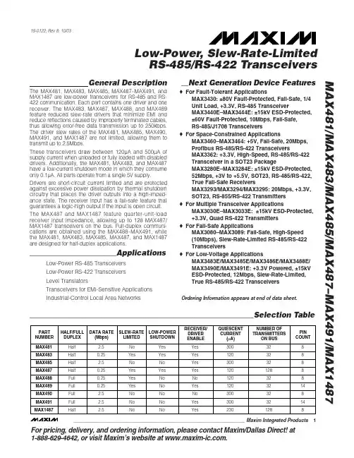
For pricing, delivery, and ordering information,please contact Maxim/Dallas Direct!at 1-888-629-4642, or visit Maxim’s website at .General DescriptionThe MAX481, MAX483, MAX485, MAX487–MAX491, and MAX1487 are low-power transceivers for RS-485 and RS-422 communication. Each part contains one driver and one receiver. The MAX483, MAX487, MAX488, and MAX489feature reduced slew-rate drivers that minimize EMI and reduce reflections caused by improperly terminated cables,thus allowing error-free data transmission up to 250kbps.The driver slew rates of the MAX481, MAX485, MAX490,MAX491, and MAX1487 are not limited, allowing them to transmit up to 2.5Mbps.These transceivers draw between 120µA and 500µA of supply current when unloaded or fully loaded with disabled drivers. Additionally, the MAX481, MAX483, and MAX487have a low-current shutdown mode in which they consume only 0.1µA. All parts operate from a single 5V supply.Drivers are short-circuit current limited and are protected against excessive power dissipation by thermal shutdown circuitry that places the driver outputs into a high-imped-ance state. The receiver input has a fail-safe feature that guarantees a logic-high output if the input is open circuit.The MAX487 and MAX1487 feature quarter-unit-load receiver input impedance, allowing up to 128 MAX487/MAX1487 transceivers on the bus. Full-duplex communi-cations are obtained using the MAX488–MAX491, while the MAX481, MAX483, MAX485, MAX487, and MAX1487are designed for half-duplex applications.________________________ApplicationsLow-Power RS-485 Transceivers Low-Power RS-422 Transceivers Level TranslatorsTransceivers for EMI-Sensitive Applications Industrial-Control Local Area Networks__Next Generation Device Features♦For Fault-Tolerant ApplicationsMAX3430: ±80V Fault-Protected, Fail-Safe, 1/4Unit Load, +3.3V, RS-485 TransceiverMAX3440E–MAX3444E: ±15kV ESD-Protected,±60V Fault-Protected, 10Mbps, Fail-Safe, RS-485/J1708 Transceivers♦For Space-Constrained ApplicationsMAX3460–MAX3464: +5V, Fail-Safe, 20Mbps,Profibus RS-485/RS-422 TransceiversMAX3362: +3.3V, High-Speed, RS-485/RS-422Transceiver in a SOT23 PackageMAX3280E–MAX3284E: ±15kV ESD-Protected,52Mbps, +3V to +5.5V, SOT23, RS-485/RS-422,True Fail-Safe ReceiversMAX3293/MAX3294/MAX3295: 20Mbps, +3.3V,SOT23, RS-855/RS-422 Transmitters ♦For Multiple Transceiver ApplicationsMAX3030E–MAX3033E: ±15kV ESD-Protected,+3.3V, Quad RS-422 Transmitters ♦For Fail-Safe ApplicationsMAX3080–MAX3089: Fail-Safe, High-Speed (10Mbps), Slew-Rate-Limited RS-485/RS-422Transceivers♦For Low-Voltage ApplicationsMAX3483E/MAX3485E/MAX3486E/MAX3488E/MAX3490E/MAX3491E: +3.3V Powered, ±15kV ESD-Protected, 12Mbps, Slew-Rate-Limited,True RS-485/RS-422 TransceiversMAX481/MAX483/MAX485/MAX487–MAX491/MAX1487Low-Power, Slew-Rate-Limited RS-485/RS-422 Transceivers______________________________________________________________Selection Table19-0122; Rev 8; 10/03Ordering Information appears at end of data sheet.M A X 481/M A X 483/M A X 485/M A X 487–M A X 491/M A X 1487Low-Power, Slew-Rate-Limited RS-485/RS-422 Transceivers 2_______________________________________________________________________________________ABSOLUTE MAXIMUM RATINGSSupply Voltage (V CC ).............................................................12V Control Input Voltage (RE , DE)...................-0.5V to (V CC + 0.5V)Driver Input Voltage (DI).............................-0.5V to (V CC + 0.5V)Driver Output Voltage (A, B)...................................-8V to +12.5V Receiver Input Voltage (A, B).................................-8V to +12.5V Receiver Output Voltage (RO).....................-0.5V to (V CC +0.5V)Continuous Power Dissipation (T A = +70°C)8-Pin Plastic DIP (derate 9.09mW/°C above +70°C)....727mW 14-Pin Plastic DIP (derate 10.00mW/°C above +70°C)..800mW 8-Pin SO (derate 5.88mW/°C above +70°C).................471mW14-Pin SO (derate 8.33mW/°C above +70°C)...............667mW 8-Pin µMAX (derate 4.1mW/°C above +70°C)..............830mW 8-Pin CERDIP (derate 8.00mW/°C above +70°C).........640mW 14-Pin CERDIP (derate 9.09mW/°C above +70°C).......727mW Operating Temperature RangesMAX4_ _C_ _/MAX1487C_ A...............................0°C to +70°C MAX4__E_ _/MAX1487E_ A.............................-40°C to +85°C MAX4__MJ_/MAX1487MJA...........................-55°C to +125°C Storage Temperature Range.............................-65°C to +160°C Lead Temperature (soldering, 10sec).............................+300°CDC ELECTRICAL CHARACTERISTICS(V CC = 5V ±5%, T A = T MIN to T MAX , unless otherwise noted.) (Notes 1, 2)Stresses beyond those listed under “Absolute Maximum Ratings” may cause permanent damage to the device. These are stress ratings only, and functional operation of the device at these or any other conditions beyond those indicated in the operational sections of the specifications is not implied. Exposure to absolute maximum rating conditions for extended periods may affect device reliability.V V IN = -7VV IN = 12V V IN = -7V V IN = 12V Input Current (A, B)I IN2V TH k Ω48-7V ≤V CM ≤12V, MAX487/MAX1487R INReceiver Input Resistance -7V ≤V CM ≤12V, all devices except MAX487/MAX1487R = 27Ω(RS-485), Figure 40.4V ≤V O ≤2.4VR = 50Ω(RS-422)I O = 4mA, V ID = -200mV I O = -4mA, V ID = 200mV V CM = 0V-7V ≤V CM ≤12V DE, DI, RE DE, DI, RE MAX487/MAX1487,DE = 0V, V CC = 0V or 5.25VDE, DI, RE R = 27Ωor 50Ω, Figure 4R = 27Ωor 50Ω, Figure 4R = 27Ωor 50Ω, Figure 4DE = 0V;V CC = 0V or 5.25V,all devices except MAX487/MAX1487CONDITIONSk Ω12µA ±1I OZRThree-State (high impedance)Output Current at ReceiverV 0.4V OL Receiver Output Low Voltage 3.5V OH Receiver Output High Voltage mV 70∆V TH Receiver Input Hysteresis V -0.20.2Receiver Differential Threshold Voltage-0.2mA 0.25mA-0.81.01.55V OD2Differential Driver Output (with load)V 2V 5V OD1Differential Driver Output (no load)µA±2I IN1Input CurrentV 0.8V IL Input Low Voltage V 2.0V IH Input High Voltage V 0.2∆V OD Change in Magnitude of Driver Common-Mode Output Voltage for Complementary Output States V 0.2∆V OD Change in Magnitude of Driver Differential Output Voltage for Complementary Output States V 3V OC Driver Common-Mode Output VoltageUNITS MINTYPMAX SYMBOL PARAMETERMAX481/MAX483/MAX485/MAX487–MAX491/MAX1487Low-Power, Slew-Rate-Limited RS-485/RS-422 Transceivers_______________________________________________________________________________________3SWITCHING CHARACTERISTICS—MAX481/MAX485, MAX490/MAX491, MAX1487(V CC = 5V ±5%, T A = T MIN to T MAX , unless otherwise noted.) (Notes 1, 2)DC ELECTRICAL CHARACTERISTICS (continued)(V CC = 5V ±5%, T A = T MIN to T MAX , unless otherwise noted.) (Notes 1, 2)ns 103060t PHLDriver Rise or Fall Time Figures 6 and 8, R DIFF = 54Ω, C L1= C L2= 100pF ns MAX490M, MAX491M MAX490C/E, MAX491C/E2090150MAX481, MAX485, MAX1487MAX490M, MAX491MMAX490C/E, MAX491C/E MAX481, MAX485, MAX1487Figures 6 and 8, R DIFF = 54Ω,C L1= C L2= 100pF MAX481 (Note 5)Figures 5 and 11, C RL = 15pF, S2 closedFigures 5 and 11, C RL = 15pF, S1 closed Figures 5 and 11, C RL = 15pF, S2 closed Figures 5 and 11, C RL = 15pF, S1 closed Figures 6 and 10, R DIFF = 54Ω,C L1= C L2= 100pFFigures 6 and 8,R DIFF = 54Ω,C L1= C L2= 100pF Figures 6 and 10,R DIFF = 54Ω,C L1= C L2= 100pF CONDITIONS ns 510t SKEW ns50200600t SHDNTime to ShutdownMbps 2.5f MAX Maximum Data Rate ns 2050t HZ Receiver Disable Time from High ns 103060t PLH 2050t LZ Receiver Disable Time from Low ns 2050t ZH Driver Input to Output Receiver Enable to Output High ns 2050t ZL Receiver Enable to Output Low 2090200ns ns 134070t HZ t SKD Driver Disable Time from High |t PLH - t PHL |DifferentialReceiver Skewns 4070t LZ Driver Disable Time from Low ns 4070t ZL Driver Enable to Output Low 31540ns51525ns 31540t R , t F 2090200Driver Output Skew to Output t PLH , t PHL Receiver Input to Output4070t ZH Driver Enable to Output High UNITS MIN TYP MAX SYMBOL PARAMETERFigures 7 and 9, C L = 100pF, S2 closed Figures 7 and 9, C L = 100pF, S1 closed Figures 7 and 9, C L = 15pF, S1 closed Figures 7 and 9, C L = 15pF, S2 closedM A X 481/M A X 483/M A X 485/M A X 487–M A X 491/M A X 1487Low-Power, Slew-Rate-Limited RS-485/RS-422 Transceivers 4_______________________________________________________________________________________SWITCHING CHARACTERISTICS—MAX483, MAX487/MAX488/MAX489(V CC = 5V ±5%, T A = T MIN to T MAX , unless otherwise noted.) (Notes 1, 2)SWITCHING CHARACTERISTICS—MAX481/MAX485, MAX490/MAX491, MAX1487 (continued)(V CC = 5V ±5%, T A = T MIN to T MAX , unless otherwise noted.) (Notes 1, 2)3001000Figures 7 and 9, C L = 100pF, S2 closed Figures 7 and 9, C L = 100pF, S1 closed Figures 5 and 11, C L = 15pF, S2 closed,A - B = 2VCONDITIONSns 40100t ZH(SHDN)Driver Enable from Shutdown toOutput High (MAX481)nsFigures 5 and 11, C L = 15pF, S1 closed,B - A = 2Vt ZL(SHDN)Receiver Enable from Shutdownto Output Low (MAX481)ns 40100t ZL(SHDN)Driver Enable from Shutdown toOutput Low (MAX481)ns 3001000t ZH(SHDN)Receiver Enable from Shutdownto Output High (MAX481)UNITS MINTYP MAX SYMBOLPARAMETERt PLH t SKEW Figures 6 and 8, R DIFF = 54Ω,C L1= C L2= 100pFt PHL Figures 6 and 8, R DIFF = 54Ω,C L1= C L2= 100pFDriver Input to Output Driver Output Skew to Output ns 100800ns ns 2000MAX483/MAX487, Figures 7 and 9,C L = 100pF, S2 closedt ZH(SHDN)Driver Enable from Shutdown to Output High2502000ns2500MAX483/MAX487, Figures 5 and 11,C L = 15pF, S1 closedt ZL(SHDN)Receiver Enable from Shutdown to Output Lowns 2500MAX483/MAX487, Figures 5 and 11,C L = 15pF, S2 closedt ZH(SHDN)Receiver Enable from Shutdown to Output Highns 2000MAX483/MAX487, Figures 7 and 9,C L = 100pF, S1 closedt ZL(SHDN)Driver Enable from Shutdown to Output Lowns 50200600MAX483/MAX487 (Note 5) t SHDN Time to Shutdownt PHL t PLH , t PHL < 50% of data period Figures 5 and 11, C RL = 15pF, S2 closed Figures 5 and 11, C RL = 15pF, S1 closed Figures 5 and 11, C RL = 15pF, S2 closed Figures 5 and 11, C RL = 15pF, S1 closed Figures 7 and 9, C L = 15pF, S2 closed Figures 6 and 10, R DIFF = 54Ω,C L1= C L2= 100pFFigures 7 and 9, C L = 15pF, S1 closed Figures 7 and 9, C L = 100pF, S1 closed Figures 7 and 9, C L = 100pF, S2 closed CONDITIONSkbps 250f MAX 2508002000Maximum Data Rate ns 2050t HZ Receiver Disable Time from High ns 25080020002050t LZ Receiver Disable Time from Low ns 2050t ZH Receiver Enable to Output High ns 2050t ZL Receiver Enable to Output Low ns ns 1003003000t HZ t SKD Driver Disable Time from High I t PLH - t PHL I DifferentialReceiver SkewFigures 6 and 10, R DIFF = 54Ω,C L1= C L2= 100pFns 3003000t LZ Driver Disable Time from Low ns 2502000t ZL Driver Enable to Output Low ns Figures 6 and 8, R DIFF = 54Ω,C L1= C L2= 100pFns 2502000t R , t F 2502000Driver Rise or Fall Time ns t PLH Receiver Input to Output2502000t ZH Driver Enable to Output High UNITS MIN TYP MAX SYMBOL PARAMETERMAX481/MAX483/MAX485/MAX487–MAX491/MAX1487Low-Power, Slew-Rate-Limited RS-485/RS-422 Transceivers_______________________________________________________________________________________530002.5OUTPUT CURRENT vs.RECEIVER OUTPUT LOW VOLTAGE525M A X 481-01OUTPUT LOW VOLTAGE (V)O U T P U T C U R R E N T (m A )1.515100.51.02.0203540450.90.1-50-252575RECEIVER OUTPUT LOW VOLTAGE vs.TEMPERATURE0.30.7TEMPERATURE (°C)O U T P U TL O W V O L T A G E (V )500.50.80.20.60.40100125-20-41.5 2.0 3.0 5.0OUTPUT CURRENT vs.RECEIVER OUTPUT HIGH VOLTAGE-8-16M A X 481-02OUTPUT HIGH VOLTAGE (V)O U T P U T C U R R E N T (m A )2.5 4.0-12-18-6-14-10-203.54.5 4.83.2-50-252575RECEIVER OUTPUT HIGH VOLTAGE vs.TEMPERATURE3.64.4TEMPERATURE (°C)O U T P UT H I G H V O L T A G E (V )0504.04.63.44.23.83.01001259000 1.0 3.0 4.5DRIVER OUTPUT CURRENT vs.DIFFERENTIAL OUTPUT VOLTAGE1070M A X 481-05DIFFERENTIAL OUTPUT VOLTAGE (V)O U T P U T C U R R E N T (m A )2.0 4.05030806040200.5 1.5 2.53.5 2.31.5-50-2525125DRIVER DIFFERENTIAL OUTPUT VOLTAGEvs. TEMPERATURE1.72.1TEMPERATURE (°C)D I F FE R E N T I A L O U T P U T V O L T A G E (V )751.92.21.62.01.8100502.4__________________________________________Typical Operating Characteristics(V CC = 5V, T A = +25°C, unless otherwise noted.)NOTES FOR ELECTRICAL/SWITCHING CHARACTERISTICSNote 1:All currents into device pins are positive; all currents out of device pins are negative. All voltages are referenced to deviceground unless otherwise specified.Note 2:All typical specifications are given for V CC = 5V and T A = +25°C.Note 3:Supply current specification is valid for loaded transmitters when DE = 0V.Note 4:Applies to peak current. See Typical Operating Characteristics.Note 5:The MAX481/MAX483/MAX487 are put into shutdown by bringing RE high and DE low. If the inputs are in this state for lessthan 50ns, the parts are guaranteed not to enter shutdown. If the inputs are in this state for at least 600ns, the parts are guaranteed to have entered shutdown. See Low-Power Shutdown Mode section.M A X 481/M A X 483/M A X 485/M A X 487–M A X 491/M A X 1487Low-Power, Slew-Rate-Limited RS-485/RS-422 Transceivers 6___________________________________________________________________________________________________________________Typical Operating Characteristics (continued)(V CC = 5V, T A = +25°C, unless otherwise noted.)120008OUTPUT CURRENT vs.DRIVER OUTPUT LOW VOLTAGE20100M A X 481-07OUTPUT LOW VOLTAGE (V)O U T P U T C U R R E N T (m A )6604024801012140-1200-7-5-15OUTPUT CURRENT vs.DRIVER OUTPUT HIGH VOLTAGE-20-80M A X 481-08OUTPUT HIGH VOLTAGE (V)O U T P U T C U R R E N T (m A )-31-603-6-4-2024-100-40100-40-60-2040100120MAX1487SUPPLY CURRENT vs. TEMPERATURE300TEMPERATURE (°C)S U P P L Y C U R R E N T (µA )20608050020060040000140100-50-2550100MAX481/MAX485/MAX490/MAX491SUPPLY CURRENT vs. TEMPERATURE300TEMPERATURE (°C)S U P P L Y C U R R E N T (µA )257550020060040000125100-50-2550100MAX483/MAX487–MAX489SUPPLY CURRENT vs. TEMPERATURE300TEMPERATURE (°C)S U P P L Y C U R R E N T (µA )257550020060040000125MAX481/MAX483/MAX485/MAX487–MAX491/MAX1487Low-Power, Slew-Rate-Limited RS-485/RS-422 Transceivers_______________________________________________________________________________________7______________________________________________________________Pin DescriptionFigure 1. MAX481/MAX483/MAX485/MAX487/MAX1487 Pin Configuration and Typical Operating CircuitM A X 481/M A X 483/M A X 485/M A X 487–M A X 491/M A X 1487__________Applications InformationThe MAX481/MAX483/MAX485/MAX487–MAX491 and MAX1487 are low-power transceivers for RS-485 and RS-422 communications. The MAX481, MAX485, MAX490,MAX491, and MAX1487 can transmit and receive at data rates up to 2.5Mbps, while the MAX483, MAX487,MAX488, and MAX489 are specified for data rates up to 250kbps. The MAX488–MAX491 are full-duplex trans-ceivers while the MAX481, MAX483, MAX485, MAX487,and MAX1487 are half-duplex. In addition, Driver Enable (DE) and Receiver Enable (RE) pins are included on the MAX481, MAX483, MAX485, MAX487, MAX489,MAX491, and MAX1487. When disabled, the driver and receiver outputs are high impedance.MAX487/MAX1487:128 Transceivers on the BusThe 48k Ω, 1/4-unit-load receiver input impedance of the MAX487 and MAX1487 allows up to 128 transceivers on a bus, compared to the 1-unit load (12k Ωinput impedance) of standard RS-485 drivers (32 trans-ceivers maximum). Any combination of MAX487/MAX1487 and other RS-485 transceivers with a total of 32 unit loads or less can be put on the bus. The MAX481/MAX483/MAX485 and MAX488–MAX491 have standard 12k ΩReceiver Input impedance.Low-Power, Slew-Rate-Limited RS-485/RS-422 Transceivers 8_______________________________________________________________________________________Figure 2. MAX488/MAX490 Pin Configuration and Typical Operating CircuitFigure 3. MAX489/MAX491 Pin Configuration and Typical Operating CircuitMAX483/MAX487/MAX488/MAX489:Reduced EMI and ReflectionsThe MAX483 and MAX487–MAX489 are slew-rate limit-ed, minimizing EMI and reducing reflections caused by improperly terminated cables. Figure 12 shows the dri-ver output waveform and its Fourier analysis of a 150kHz signal transmitted by a MAX481, MAX485,MAX490, MAX491, or MAX1487. High-frequency har-monics with large amplitudes are evident. Figure 13shows the same information displayed for a MAX483,MAX487, MAX488, or MAX489 transmitting under the same conditions. Figure 13’s high-frequency harmonics have much lower amplitudes, and the potential for EMI is significantly reduced.MAX481/MAX483/MAX485/MAX487–MAX491/MAX1487Low-Power, Slew-Rate-Limited RS-485/RS-422 Transceivers_______________________________________________________________________________________9_________________________________________________________________Test CircuitsFigure 4. Driver DC Test Load Figure 5. Receiver Timing Test LoadFigure 6. Driver/Receiver Timing Test Circuit Figure 7. Driver Timing Test LoadM A X 481/M A X 483/M A X 485/M A X 487–M A X 491/M A X 1487Low-Power, Slew-Rate-Limited RS-485/RS-422 Transceivers 10_______________________________________________________Switching Waveforms_________________Function Tables (MAX481/MAX483/MAX485/MAX487/MAX1487)Figure 8. Driver Propagation DelaysFigure 9. Driver Enable and Disable Times (except MAX488 and MAX490)Figure 10. Receiver Propagation DelaysFigure 11. Receiver Enable and Disable Times (except MAX488and MAX490)Table 1. TransmittingTable 2. ReceivingLow-Power Shutdown Mode (MAX481/MAX483/MAX487)A low-power shutdown mode is initiated by bringing both RE high and DE low. The devices will not shut down unless both the driver and receiver are disabled.In shutdown, the devices typically draw only 0.1µA of supply current.RE and DE may be driven simultaneously; the parts are guaranteed not to enter shutdown if RE is high and DE is low for less than 50ns. If the inputs are in this state for at least 600ns, the parts are guaranteed to enter shutdown.For the MAX481, MAX483, and MAX487, the t ZH and t ZL enable times assume the part was not in the low-power shutdown state (the MAX485/MAX488–MAX491and MAX1487 can not be shut down). The t ZH(SHDN)and t ZL(SHDN)enable times assume the parts were shut down (see Electrical Characteristics ).It takes the drivers and receivers longer to become enabled from the low-power shutdown state (t ZH(SHDN ), t ZL(SHDN)) than from the operating mode (t ZH , t ZL ). (The parts are in operating mode if the –R —E –,DE inputs equal a logical 0,1 or 1,1 or 0, 0.)Driver Output ProtectionExcessive output current and power dissipation caused by faults or by bus contention are prevented by two mechanisms. A foldback current limit on the output stage provides immediate protection against short cir-cuits over the whole common-mode voltage range (see Typical Operating Characteristics ). In addition, a ther-mal shutdown circuit forces the driver outputs into a high-impedance state if the die temperature rises excessively.Propagation DelayMany digital encoding schemes depend on the differ-ence between the driver and receiver propagation delay times. Typical propagation delays are shown in Figures 15–18 using Figure 14’s test circuit.The difference in receiver delay times, | t PLH - t PHL |, is typically under 13ns for the MAX481, MAX485,MAX490, MAX491, and MAX1487 and is typically less than 100ns for the MAX483 and MAX487–MAX489.The driver skew times are typically 5ns (10ns max) for the MAX481, MAX485, MAX490, MAX491, and MAX1487, and are typically 100ns (800ns max) for the MAX483 and MAX487–MAX489.MAX481/MAX483/MAX485/MAX487–MAX491/MAX1487Low-Power, Slew-Rate-Limited RS-485/RS-422 Transceivers______________________________________________________________________________________1110dB/div0Hz5MHz500kHz/div10dB/div0Hz5MHz500kHz/divFigure 12. Driver Output Waveform and FFT Plot of MAX481/MAX485/MAX490/MAX491/MAX1487 Transmitting a 150kHz SignalFigure 13. Driver Output Waveform and FFT Plot of MAX483/MAX487–MAX489 Transmitting a 150kHz SignalM A X 481/M A X 483/M A X 485/M A X 487–M A X 491/M A X 1487Low-Power, Slew-Rate-Limited RS-485/RS-422 Transceivers 12______________________________________________________________________________________V CC = 5V T A = +25°CV CC = 5V T A = +25°CV CC = 5V T A = +25°CV CC = 5V T A = +25°CFigure 14. Receiver Propagation Delay Test CircuitFigure 15. MAX481/MAX485/MAX490/MAX491/MAX1487Receiver t PHLFigure 16. MAX481/MAX485/MAX490/MAX491/MAX1487Receiver t PLHPHL Figure 18. MAX483, MAX487–MAX489 Receiver t PLHLine Length vs. Data RateThe RS-485/RS-422 standard covers line lengths up to 4000 feet. For line lengths greater than 4000 feet, see Figure 23.Figures 19 and 20 show the system differential voltage for the parts driving 4000 feet of 26AWG twisted-pair wire at 110kHz into 120Ωloads.Typical ApplicationsThe MAX481, MAX483, MAX485, MAX487–MAX491, and MAX1487 transceivers are designed for bidirectional data communications on multipoint bus transmission lines.Figures 21 and 22 show typical network applications circuits. These parts can also be used as line repeaters, with cable lengths longer than 4000 feet, as shown in Figure 23.To minimize reflections, the line should be terminated at both ends in its characteristic impedance, and stub lengths off the main line should be kept as short as possi-ble. The slew-rate-limited MAX483 and MAX487–MAX489are more tolerant of imperfect termination.MAX481/MAX483/MAX485/MAX487–MAX491/MAX1487Low-Power, Slew-Rate-Limited RS-485/RS-422 Transceivers______________________________________________________________________________________13DIV Y -V ZRO5V 0V1V0V -1V5V 0V2µs/divFigure 19. MAX481/MAX485/MAX490/MAX491/MAX1487 System Differential Voltage at 110kHz Driving 4000ft of Cable Figure 20. MAX483, MAX487–MAX489 System Differential Voltage at 110kHz Driving 4000ft of CableFigure 21. MAX481/MAX483/MAX485/MAX487/MAX1487 Typical Half-Duplex RS-485 NetworkM A X 481/M A X 483/M A X 485/M A X 487–M A X 491/M A X 1487Low-Power, Slew-Rate-Limited RS-485/RS-422 Transceivers 14______________________________________________________________________________________Figure 22. MAX488–MAX491 Full-Duplex RS-485 NetworkFigure 23. Line Repeater for MAX488–MAX491Isolated RS-485For isolated RS-485 applications, see the MAX253 and MAX1480 data sheets.MAX481/MAX483/MAX485/MAX487–MAX491/MAX1487Low-Power, Slew-Rate-Limited RS-485/RS-422 Transceivers______________________________________________________________________________________15_______________Ordering Information_________________Chip TopographiesMAX481/MAX483/MAX485/MAX487/MAX1487N.C. RO 0.054"(1.372mm)0.080"(2.032mm)DE DIGND B N.C.V CCARE * Contact factory for dice specifications.__Ordering Information (continued)M A X 481/M A X 483/M A X 485/M A X 487–M A X 491/M A X 1487Low-Power, Slew-Rate-Limited RS-485/RS-422 Transceivers 16______________________________________________________________________________________TRANSISTOR COUNT: 248SUBSTRATE CONNECTED TO GNDMAX488/MAX490B RO 0.054"(1.372mm)0.080"(2.032mm)N.C. DIGND Z A V CCYN.C._____________________________________________Chip Topographies (continued)MAX489/MAX491B RO 0.054"(1.372mm)0.080"(2.032mm)DE DIGND Z A V CCYREMAX481/MAX483/MAX485/MAX487–MAX491/MAX1487Low-Power, Slew-Rate-Limited RS-485/RS-422 Transceivers______________________________________________________________________________________17Package Information(The package drawing(s) in this data sheet may not reflect the most current specifications. For the latest package outline information go to /packages .)S O I C N .E P SM A X 481/M A X 483/M A X 485/M A X 487–M A X 491/M A X 1487Low-Power, Slew-Rate-Limited RS-485/RS-422 Transceivers 18______________________________________________________________________________________Package Information (continued)(The package drawing(s) in this data sheet may not reflect the most current specifications. For the latest package outline information go to /packages .)MAX481/MAX483/MAX485/MAX487–MAX491Low-Power, Slew-Rate-Limited RS-485/RS-422 TransceiversMaxim cannot assume responsibility for use of any circuitry other than circuitry entirely embodied in a Maxim product. No circuit patent licenses are implied. Maxim reserves the right to change the circuitry and specifications without notice at any time.Maxim Integrated Products, 120 San Gabriel Drive, Sunnyvale, CA 94086 408-737-7600 ____________________19©2003 Maxim Integrated ProductsPrinted USAis a registered trademark of Maxim Integrated Products.M A X 481/M A X 483/M A X 485/M A X 487–M A X 491/M A X 1487P D I P N .E PSPackage Information (continued)(The package drawing(s) in this data sheet may not reflect the most current specifications. For the latest package outline information go to /packages .)。
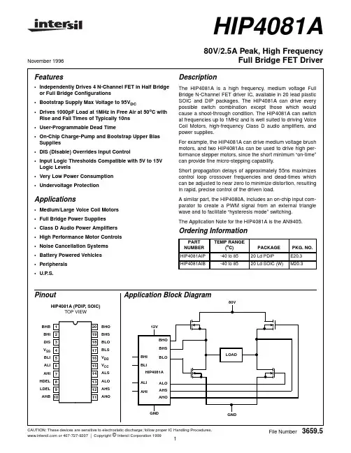
HIP4081A80V/2.5A Peak, High FrequencyFull Bridge FET DriverDescriptionThe HIP4081A is a high frequency, medium voltage Full Bridge N-Channel FET driver IC, available in 20 lead plastic SOIC and DIP packages. The HIP4081A can drive every possible switch combination except those which would cause a shoot-through condition. The HIP4081A can switch at frequencies up to 1MHz and is well suited to driving Voice Coil Motors, high-frequency Class D audio amplifiers, and power supplies.For example, the HIP4081A can drive medium voltage brush motors, and two HIP4081As can be used to drive high per-formance stepper motors, since the short minimum “on-time”can provide fine micro-stepping capability.Short propagation delays of approximately 55ns maximizes control loop crossover frequencies and dead-times which can be adjusted to near zero to minimize distortion, resulting in rapid, precise control of the driven load.A similar part, the HIP4080A, includes an on-chip input com-parator to create a PWM signal from an external triangle wave and to facilitate “hysteresis mode” switching.The Application Note for the HIP4081A is the AN9405.Ordering InformationPART NUMBER TEMP RANGE(o C)PACKAGE PKG. NO.HIP4081AIP -40 to 8520 Ld PDIP E20.3HIP4081AIB-40 to 8520 Ld SOIC (W)M20.3Features•Independently Drives 4 N-Channel FET in Half Bridge or Full Bridge Configurations •Bootstrap Supply Max Voltage to 95V DC•Drives 1000pF Load at 1MHz in Free Air at 50o C with Rise and Fall Times of Typically 10ns •User-Programmable Dead Time•On-Chip Charge-Pump and Bootstrap Upper Bias Supplies •DIS (Disable) Overrides Input Control•Input Logic Thresholds Compatible with 5V to 15V Logic Levels •Very Low Power Consumption •Undervoltage ProtectionApplications•Medium/Large Voice Coil Motors •Full Bridge Power Supplies •Class D Audio Power Amplifiers •High Performance Motor Controls •Noise Cancellation Systems •Battery Powered Vehicles •Peripherals •U.P .S.November 1996PinoutHIP4081A (PDIP, SOIC)TOP VIEW1112131415161718201910987654321BHB BHI DIS V SS BLI ALI HDEL AHI LDELAHB BHO BLO BLS V DD BHS V CC ALS ALO AHS AHOApplication Block Diagram80VGNDLOADHIP4081A GND12VAHIALI BLIBHI BLOBHSBHO ALO AHS AHO File Number3659.5CAUTION: These devices are sensitive to electrostatic discharge; follow proper IC Handling Procedures.Functional Block Diagram(1/2 HIP4081A)Typical Application(PWM Mode Switching)CHARGE PUMP V DD AHIDIS ALIHDEL LDEL V SSTURN-ON DELAYTURN-ON DELAYDRIVERDRIVERAHB AHOAHS V CCALOALS C BFTO V DD (PIN 16)C BSD BSHIGH VOLTAGE BUS ≤ 80V DC+12V DC LEVEL SHIFT AND LATCH14101112151316736894BIAS SUPPLYUNDER-VOLTAGE1112131415161718201910987654321BHBBHI DIS V SS BLI ALI HDEL AHILDEL AHBBHO BLO BLS V DD BHS V CC ALS ALO AHS AHO 80V12V+-12V DISGND6VGNDTO OPTIONALCURRENT CONTROLLERPWM LOADINPUTH I P 4081/H I P 4081AAbsolute Maximum Ratings Thermal InformationSupply Voltage, V DD and V CC. . . . . . . . . . . . . . . . . . . .-0.3V to 16V Logic I/O Voltages . . . . . . . . . . . . . . . . . . . . . . .-0.3V to V DD +0.3V Voltage on AHS, BHS. . . .-6.0V (Transient) to 80V (25o C to 125o C) Voltage on AHS, BHS. . .-6.0V (T ransient) to 70V (-55o C to 125o C) Voltage on ALS, BLS . . . . . . .-2.0V (Transient) to +2.0V (Transient) Voltage on AHB, BHB. . . . . . . . .V AHS, BHS -0.3V to V AHS, BHS +V DD Voltage on ALO, BLO. . . . . . . . . . . . .V ALS, BLS -0.3V to V CC +0.3V Voltage on AHO, BHO . . . . . . .V AHS, BHS -0.3V to V AHB, BHB +0.3V Input Current, HDEL and LDEL . . . . . . . . . . . . . . . . . .-5mA to 0mA Phase Slew Rate . . . . . . . . . . . . . . . . . . . . . . . . . . . . . . . . . .20V/ns NOTE: All Voltages relative to V SS, unless otherwise specified.Thermal Resistance (T ypical, Note 1)θJA (o C/W) SOIC Package. . . . . . . . . . . . . . . . . . . . . . . . . . . . .85 DIP Package . . . . . . . . . . . . . . . . . . . . . . . . . . . . . .75 Storage Temperature Range. . . . . . . . . . . . . . . . . . .-65o C to 150o C Operating Max. Junction Temperature . . . . . . . . . . . . . . . . . .125o C Lead T emperature (Soldering 10s)) . . . . . . . . . . . . . . . . . . . .300o C (For SOIC - Lead Tips OnlyCAUTION: Stresses above those listed in “Absolute Maximum Ratings” may cause permanent damage to the device. This is a stress only rating and operation of the device at these or any other conditions above those indicated in the operational sections of this specification is not implied.NOTE:1.θJA is measured with the component mounted on an evaluation PC board in free air.Operating ConditionsSupply Voltage, V DD and V CC. . . . . . . . . . . . . . . . . . .+9.5V to +15V Voltage on ALS, BLS . . . . . . . . . . . . . . . . . . . . . . . . .-1.0V to +1.0V Voltage on AHB, BHB. . . . . . . . . .V AHS, BHS +5V to V AHS, BHS +15V Input Current, HDEL and LDEL. . . . . . . . . . . . . . . .-500µA to -50µA Operating Ambient Temperature Range . . . . . . . . . . .-40o C to 85o CElectrical Specifications V DD = V CC = V AHB = V BHB = 12V, V SS = V ALS = V BLS = V AHS = V BHS = 0V, R HDEL = R LDEL = 100K andT A = 25o C, Unless Otherwise SpecifiedPARAMETER SYMBOL TEST CONDITIONST J = 25o CT JS = -40o CTO 125o CUNITS MIN TYP MAX MIN MAXSUPPLY CURRENTS AND CHARGE PUMPSV DD Quiescent Current I DD All inputs = 0V8.5 10.514.57.514.5 mA V DD Operating Current I DDO Outputs switching f = 500kHz9.512.515.58.515.5 mA V CC Quiescent Current I CC All Inputs = 0V, I ALO = I BLO = 0-0.110-20µA V CC Operating Current I CCO f = 500kHz, No Load1 1.25 2.00.83mAAHB, BHB Quiescent Current -Qpump Output Current I AHB, I BHB All Inputs = 0V, I AHO = I BHO = 0V DD = V CC = V AHB = V BHB= 10V-50-30-11-60-10µAAHB, BHB Operating Current I AHBO, I BHBO f = 500kHz, No Load0.6 1.2 1.50.5 1.9mAAHS, BHS, AHB, BHB Leakage Current I HLK V BHS = V AHS = 80V,V AHB = V BHB = 93V-0.02 1.0-10µAAHB-AHS, BHB-BHS Qpump Output Voltage V AHB-V AHSV BHB-V BHSI AHB = I AHB = 0, No Load11.512.614.010.514.5VINPUT PINS: ALI, BLI, AHI, BHI, AND DISLow Level Input Voltage V IL Full Operating Conditions-- 1.0-0.8V High Level Input Voltage V IH Full Operating Conditions 2.5-- 2.7-V Input Voltage Hysteresis-35---mV Low Level Input Current I IL V IN = 0V, Full Operating Conditions-130-100-75-135-65µA High Level Input Current I IH V IN = 5V, Full Operating Conditions-1-+1-10+10µA TURN-ON DELAY PINS: LDEL AND HDELLDEL, HDEL Voltage V HDEL, V LDEL I HDEL = I LDEL = -100µA 4.9 5.1 5.3 4.8 5.4V GATE DRIVER OUTPUT PINS: ALO, BLO, AHO, AND BHOLow Level Output Voltage V OL I OUT = 100mA0.70.85 1.00.5 1.1V High Level Output Voltage V CC-V OH I OUT = -100mA0.80.95 1.10.5 1.2V Peak Pullup Current I O+V OUT = 0V 1.7 2.6 3.8 1.4 4.1A Peak Pulldown Current I O-V OUT = 12V 1.7 2.4 3.3 1.3 3.6AUndervoltage, Rising Threshold UV+8.18.89.48.09.5V Undervoltage, Falling Threshold UV-7.68.38.97.59.0V Undervoltage, HysteresisHYS0.250.40.650.20.7VSwitching SpecificationsV DD = V CC = V AHB = V BHB = 12V , V SS = V ALS = V BLS = V AHS = V BHS = 0V , R HDEL = R LDEL = 10K,C L = 1000pF .PARAMETERSYMBOL TEST CONDITIONS T J= 25o C T JS = -40o C TO 125o C UNITS MIN TYP MAX MIN MAX Lower Turn-off Propagation Delay (ALI-ALO, BLI-BLO)T LPHL -3060-80ns Upper Turn-off Propagation Delay (AHI-AHO, BHI-BHO)T HPHL -3570-90ns Lower Turn-on Propagation Delay (ALI-ALO, BLI-BLO)T LPLH R HDEL =R LDEL = 10K -4570-90ns Upper Turn-on Propagation Delay (AHI-AHO, BHI-BHO)T HPLH R HDEL =R LDEL = 10K-6090-110ns Rise Time T R -1025-35ns Fall TimeT F -1025-35ns Turn-on Input Pulse Width T PWIN-ON R HDEL =R LDEL = 10K 50--50-ns Turn-off Input Pulse Width T PWIN-OFF R HDEL =R LDEL = 10K 40--40-ns Turn-on Output Pulse Width T PWOUT -ON R HDEL =R LDEL = 10K 40--40-ns Turn-off Output Pulse Width T PWOUT -OFF R HDEL =R LDEL = 10K30--30-ns Disable Turn-off Propagation Delay (DIS - Lower Outputs)T DISLOW -4575-95ns Disable Turn-off Propagation Delay (DIS - Upper Outputs)T DISHIGH -5585-105ns Disable to Lower Turn-on Propagation Delay (DIS - ALO and BLO)T DLPLH -4070-90ns Refresh Pulse Width (ALO and BLO)T REF-PW 240410550200600ns Disable to Upper Enable (DIS - AHO and BHO)T UEN-450620-690nsTRUTH TABLEINPUTOUTPUTALI, BLIAHI, BHIU/V DIS ALO, BLOAHO, BHOX X X 1001X 0010010001000000XX1XNOTE:X signifies that input can be either a “1” or “0”.Electrical SpecificationsV DD = V CC = V AHB = V BHB = 12V , V SS = V ALS = V BLS = V AHS = V BHS = 0V , R HDEL = R LDEL = 100K and T A = 25o C, Unless Otherwise Specified (Continued)PARAMETERSYMBOL TEST CONDITIONST J = 25o CT JS = -40o C TO 125o C UNITS MIN TYP MAX MIN MAXPin DescriptionsPINNUMBER SYMBOL DESCRIPTION1BHB B High-side Bootstrap supply. External bootstrap diode and capacitor are required. Connect cathode of boot-strap diode and positive side of bootstrap capacitor to this pin. Internal charge pump supplies 30µA out of thispin to maintain bootstrap supply. Internal circuitry clamps the bootstrap supply to approximately 12.8V.2BHI B High-side Input. Logic level input that controls BHO driver (Pin 20). BLI (Pin 5) high level input overrides BHI high level input to prevent half-bridge shoot-through, see T ruth T able. DIS (Pin 3) high level input overrides BHIhigh level input. The pin can be driven by signal levels of 0V to 15V (no greater than V DD). An internal 100µApull-up to V DD will hold BHI high, so no connection is required if high-side and low-side outputs are to be con-trolled by the low-side input.3DIS DISable input. Logic level input that when taken high sets all four outputs low. DIS high overrides all other inputs.When DIS is taken low the outputs are controlled by the other inputs. The pin can be driven by signal levels of0V to 15V (no greater than V DD). An internal 100µA pull-up to V DD will hold DIS high if this pin is not driven.4V SS Chip negative supply, generally will be ground.5BLI B Low-side Input. Logic level input that controls BLO driver (Pin 18). If BHI (Pin 2) is driven high or not connected externally then BLI controls both BLO and BHO drivers, with dead time set by delay currents at HDEL and LDEL(Pin 8 and 9). DIS (Pin 3) high level input overrides BLI high level input. The pin can be driven by signal levelsof 0V to 15V (no greater than V DD). An internal 100µA pull-up to V DD will hold BLI high if this pin is not driven.6ALI A Low-side Input. Logic level input that controls ALO driver (Pin 13). If AHI (Pin 7) is driven high or not connected externally then ALI controls both ALO and AHO drivers, with dead time set by delay currents at HDEL and LDEL(Pin 8 and 9). DIS (Pin 3) high level input overrides ALI high level input. The pin can be driven by signal levelsof 0V to 15V (no greater than V DD). An internal 100µA pull-up to V DD will hold ALI high if this pin is not driven.7AHI A High-side Input. Logic level input that controls AHO driver (Pin 11). ALI (Pin 6) high level input overrides AHI high level input to prevent half-bridge shoot-through, see T ruth T able. DIS (Pin 3) high level input overrides AHIhigh level input. The pin can be driven by signal levels of 0V to 15V (no greater than V DD). An internal 100µApull-up to V DD will hold AHI high, so no connection is required if high-side and low-side outputs are to be con-trolled by the low-side input.8HDEL High-side turn-on DELay. Connect resistor from this pin to V SS to set timing current that defines the turn-on de-lay of both high-side drivers. The low-side drivers turn-off with no adjustable delay, so the HDEL resistor guar-antees no shoot-through by delaying the turn-on of the high-side drivers. HDEL reference voltage isapproximately 5.1V.9LDEL Low-side turn-on DELay. Connect resistor from this pin to V SS to set timing current that defines the turn-on delay of both low-side drivers. The high-side drivers turn-off with no adjustable delay, so the LDEL resistor guaranteesno shoot-through by delaying the turn-on of the low-side drivers. LDEL reference voltage is approximately 5.1V.10AHB A High-side Bootstrap supply. External bootstrap diode and capacitor are required. Connect cathode of boot-strap diode and positive side of bootstrap capacitor to this pin. Internal charge pump supplies 30µA out of thispin to maintain bootstrap supply. Internal circuitry clamps the bootstrap supply to approximately 12.8V.11AHO A High-side Output. Connect to gate of A High-side power MOSFET.12AHS A High-side Source connection. Connect to source of A High-side power MOSFET. Connect negative side of bootstrap capacitor to this pin.13ALO A Low-side Output. Connect to gate of A Low-side power MOSFET.14ALS A Low-side Source connection. Connect to source of A Low-side power MOSFET.15V CC Positive supply to gate drivers. Must be same potential as V DD (Pin 16). Connect to anodes of two bootstrap diodes.16V DD Positive supply to lower gate drivers. Must be same potential as V CC (Pin 15). De-couple this pin to V SS (Pin 4).17BLS B Low-side Source connection. Connect to source of B Low-side power MOSFET.18BLO B Low-side Output. Connect to gate of B Low-side power MOSFET.19BHS B High-side Source connection. Connect to source of B High-side power MOSFET. Connect negative side of bootstrap capacitor to this pin.20BHO B High-side Output. Connect to gate of B High-side power MOSFET.Timing DiagramsFIGURE 1.INDEPENDENT MODEFIGURE 2.BISTATE MODEFIGURE 3.DISABLE FUNCTIONU/V = DIS = 0XLIXHIXLOXHOT LPHLT HPHLT HPLH T LPLHT R(10% - 90%)T F(10% - 90%)X = A OR B, A AND B HALVES OF BRIDGE CONTROLLER ARE INDEPENDENTU/V = DIS = 0XLIXHI = HI OR NOT CONNECTEDXLOXHOU/V OR DISXLIXHIXLOXHOT DLPLHT DIST UENT REF-PWFIGURE 4.QUIESCENT I DD SUPPL Y CURRENT vs V DD SUPPLYVOLTAGEFIGURE 5.I DDO , NO-LOAD I DD SUPPLY CURRENT vsFREQUENCY (kHz)FIGURE 6.SIDE A, B FLOATING SUPPLY BIAS CURRENT vsFREQUENCY (LOAD = 1000pF)FIGURE 7.I CCO , NO-LOAD I CC SUPPLY CURRENT vsFREQUENCY (kHz) TEMPERATUREFIGURE 8.I AHB , I BHB , NO-LOAD FLOATING SUPPLY BIASCURRENT vs FREQUENCY FIGURE 9.ALI, BLI, AHI, BHI LOW LEVEL INPUT CURRENT I ILvs TEMPERATURE681012142.04.06.08.010.012.014.0I D D S U P P L Y C U R R E N T (m A )V DD SUPPL Y VOLTAGE (V)10020030040050060070080090010008.08.59.09.510.010.511.0I D D S U P P L Y C U R R E N T (m A )SWITCHING FREQUENCY (kHz)10020030040050060070080090010000.05.010.015.020.025.030.0F L O A T I N G S U P P L Y B I A S C U R R E N T (m A )SWITCHING FREQUENCY (kHz)10020030040050060070080090010000.01.02.03.04.05.0I C C S U P P L Y C U R R E N T (m A )SWITCHING FREQUENCY (kHz)75o C 25o C125o C -40o C0o C 0.511.522.52006008001000400F L O A T I N G S U P P L Y B I A S C U R R E N T (m A )SWITCHING FREQUENCY (kHz)-50-250255075100125-120-110-100-90L O W L E V E L I N P U T C U R R E N T (µA )JUNCTION TEMPERATURE (o C)FIGURE 10.AHB - AHS, BHB - BHS NO-LOAD CHARGE PUMPVOLTAGE vs TEMPERATUREFIGURE 11.UPPER DISABLE TURN-OFF PROPAGATIONDELAY T DISHIGH vs TEMPERATUREFIGURE 12.DISABLE TO UPPER ENABLE, T UEN ,PROPAGATION DELAY vs TEMPERATUREFIGURE 13.LOWER DISABLE TURN-OFF PROPAGATIONDELAY T DISLOW vs TEMPERATUREFIGURE 14.T REF-PW REFRESH PULSE WIDTH vsTEMPERATURE FIGURE 15.DISABLE TO LOWER ENABLE T DLPLHPROPAGATION DELAY vs TEMPERATURE-40-202040608010012010.011.012.013.014.015.0N O -L O A D F L O A T I N G C H A R G E P U M P V O L T A G E (V )JUNCTION TEMPERATURE (oC)-40-20020406080100120304050607080P R O P A G A T I O N D E L A Y (n s )JUNCTION TEMPERATURE (o C)425450475500525-50-25255075100125150JUNCTION TEMPERATURE (o C)P R O P A G A T I O N D E L A Y (n s )-40-20020406080100120304050607080P R O P A G A T I O N D E L A Y (n s )JUNCTION TEMPERATURE (o C)350375400425450-50-25255075100125150R E F R E S H P U L S E W I D T H (n s )JUNCTION TEMPERATURE (o C)-40-202040608010012020304050607080P R O P A G A T I O N D E L A Y (n s )JUNCTION TEMPERATURE (o C)FIGURE 16.UPPER TURN-OFF PROPAGATION DELAY T HPHL vsTEMPERATURE FIGURE 17.UPPER TURN-ON PROPAGATION DELAY T HPLH vsTEMPERATUREFIGURE 18.LOWER TURN-OFF PROPAGATION DELAY T LPHL vsTEMPERATUREFIGURE 19.LOWER TURN-ON PROPAGATION DELAY T LPLH vsTEMPERATUREFIGURE 20.GATE DRIVE FALL TIME T F vs TEMPERATURE FIGURE 21.GATE DRIVE RISE TIME T R vs TEMPERATURETypical Performance CurvesV DD = V CC = V AHB = V BHB = 12V , V SS = V ALS = V BLS = V AHS = V BHS = 0V , R HDEL = R LDEL =10K and T A = 25o C, Unless Otherwise Specified (Continued)-40-202040608010012020304050607080P R O P A G A T I O N D E L A Y (n s )JUNCTION TEMPERATURE (o C)-40-2002040608010012020304050607080P R O P A G A T I O N D E L A Y (n s )JUNCTION TEMPERATURE (o C)-40-202040608010012020304050607080P R O P A G A T I O N D E L A Y (n s )JUNCTION TEMPERATURE (o C)-40-202040608010012020304050607080P R O P A G A T I O N D E L A Y (n s )JUNCTION TEMPERATURE (o C)-40-20020*********1208.59.510.511.512.513.5G A T E D R I V E F A L L T I M E (n s )JUNCTION TEMPERATURE (oC)-40-200204060801001208.59.510.511.512.513.5T U R N -O N R I S E T I M E (n s )JUNCTION TEMPERATURE (o C)Typical Performance CurvesV DD = V CC = V AHB = V BHB = 12V , V SS = V ALS = V BLS = V AHS = V BHS = 0V , R HDEL = R LDEL =100K and T A = 25o C, Unless Otherwise SpecifiedFIGURE 22.V LDEL , V HDEL VOLTAGE vs TEMPERATUREFIGURE 23.HIGH LEVEL OUTPUT VOLTAGE V CC - V OH vs BIASSUPPL Y AND TEMPERATURE AT 100mAFIGURE 24.LOW LEVEL OUTPUT VOLTAGE V OL vs BIASSUPPLY AND TEMPERATURE AT 100mAFIGURE 25.PEAK PULLDOWN CURRENT I O vs BIAS SUPPL YVOLTAGEFIGURE 26.PEAK PULLUP CURRENT I O+ vs BIAS SUPPLYVOLTAGEFIGURE 27.LOW VOLTAGE BIAS CURRENT I DD (LESSQUIESCENT COMPONENT) vs FREQUENCY AND GATE LOAD CAPACITANCE-40-20020*********1204.04.55.05.56.0H D E L , L D E L I N P U T V O L T A G E (V )JUNCTION TEMPERATURE (o C)101214250500750100012501500V C C - V O H (m V )BIAS SUPPLY VOLTAGE (V)75o C 25o C125o C-40o C 0o C 12140250500750100012501500V O L (m V )BIAS SUPPL Y VOLTAGE (V)1075o C 25o C125o C-40o C0o C 6789101112131415160.00.51.01.52.02.53.03.5G A T E D R I V E S I N K C U R R E N T (A )V DD , V CC , V AHB , V BHB (V)6789101112131415160.00.51.01.52.02.53.03.5G A T E D R I V E S I N K C U R R E N T (A )V DD , V CC , V AHB , V BHB (V)11010010002520505002000.11101005005050.52002020.2L O W V O L T A G E B I A S C U R R E N T (m A )SWITCHING FREQUENCY (kHz)100pF1,000pF 10,000pF 3,000pFHIP4081AFIGURE 28.HIGH VOLTAGE LEVEL-SHIFT CURRENT vs FREQUENCY AND BUS VOLTAGEFIGURE 29.UNDERVOLTAGE LOCKOUT vs TEMPERATUREFIGURE 30.MINIMUM DEAD-TIME vs DEL RESISTANCETypical Performance CurvesV DD = V CC = V AHB = V BHB = 12V , V SS = V ALS = V BLS = V AHS = V BHS = 0V , R HDEL = R LDEL =100K and T A = 25o C, Unless Otherwise Specified (Continued)10100100020502005001010010002050200500L E V E L -S H I F T C U R R E N T (µA )SWITCHING FREQUENCY (kHz)8.28.48.68.89.05025255075100125150UV+UV-TEMPERATURE (o C)B I A S S U P P L Y V O L T A G E , V D D (V )1050100150200250306090120150HDEL/LDEL RESISTANCE (k Ω)D E A D -T I M E (n s )E20.3 (JEDEC MS-001-AD ISSUE D)20 LEAD DUAL-IN-LINE PLASTIC PACKAGESYMBOLINCHESMILLIMETERS NOTES MIN MAX MIN MAX A -0.210- 5.334A10.015-0.39-4A20.1150.195 2.93 4.95-B 0.0140.0220.3560.558-B10.0450.070 1.55 1.778C 0.0080.0140.2040.355-D 0.980 1.06024.8926.95D10.005-0.13-5E 0.3000.3257.628.256E10.2400.2806.107.115e 0.100 BSC 2.54 BSC -e A 0.300 BSC 7.62 BSC6e B -0.430-10.927L 0.1150.1502.933.814N20209Rev. 0 12/93NOTES:1.Controlling Dimensions: INCH. In case of conflict betweenEnglish and Metric dimensions, the inch dimensions control.2.Dimensioning and tolerancing per ANSI Y14.5M -1982.3.Symbols are defined in the “MO Series Symbol List” in Section 2.2 of Publication No. 95.4.Dimensions A, A1 and L are measured with the package seated in JEDEC seating plane gauge GS -3.5.D, D1, and E1 dimensions do not include mold flash or protru-sions. Mold flash or protrusions shall not exceed 0.010 inch (0.25mm).6.E and are measured with the leads constrained to be per-pendicular to datum .7.e B and e C are measured at the lead tips with the leads uncon-strained. e C must be zero or greater.8.B1 maximum dimensions do not include dambar protrusions.Dambar protrusions shall not exceed 0.010 inch (0.25mm).9.N is the maximum number of terminal positions.10.Corner leads (1, N, N/2 and N/2 + 1) for E8.3, E16.3, E18.3,E28.3, E42.6 will have a B1 dimension of 0.030 - 0.045 inch (0.76 - 1.14mm).C L Ee ACe Be C-B-E1INDEX 123N/2NAREASEATING BASE PLANE PLANE-C-D1B1BeDD1AA2L A1-A-0.010 (0.25)C A MB Se A -C-All Intersil semiconductor products are manufactured, assembled and tested under ISO9000 quality systems certification.Intersil products are sold by description only. Intersil Corporation reserves the right to make changes in circuit design and/or specifications at any time without notice. Accordingly, the reader is cautioned to verify that data sheets are current before placing orders. Information furnished by Intersil is believed to be accurate and reliable. However, no responsibility is assumed by Intersil or its subsidiaries for its use; nor for any infringements of patents or other rights of third parties which may result from its use. No license is granted by implication or otherwise under any patent or patent rights of Intersil or its subsidiaries.For information regarding Intersil Corporation and its products, see web site Sales Office HeadquartersNORTH AMERICA Intersil CorporationP. O. Box 883, Mail Stop 53-204Melbourne, FL 32902TEL:(407) 724-7000FAX: (407) 724-7240EUROPE Intersil SAMercure Center100, Rue de la Fusee 1130 Brussels, Belgium TEL: (32) 2.724.2111FAX: (32) 2.724.22.05ASIAIntersil (Taiwan) Ltd.Taiwan Limited7F-6, No. 101 Fu Hsing North Road Taipei, Taiwan Republic of ChinaTEL: (886) 2 2716 9310FAX: (886) 2 2715 3029NOTES:1.Symbols are defined in the “MO Series Symbol List” in Section2.2 of Publication Number 95.2.Dimensioning and tolerancing per ANSI Y14.5M -1982.3.Dimension “D” does not include mold flash, protrusions or gate burrs. Mold flash, protrusion and gate burrs shall not exceed 0.15mm (0.006 inch) per side.4.Dimension “E” does not include interlead flash or protrusions. In-terlead flash and protrusions shall not exceed 0.25mm (0.010inch) per side.5.The chamfer on the body is optional. If it is not present, a visual index feature must be located within the crosshatched area.6.“L” is the length of terminal for soldering to a substrate.7.“N” is the number of terminal positions.8.Terminal numbers are shown for reference only.9.The lead width “B”, as measured 0.36mm (0.014 inch) or greater above the seating plane, shall not exceed a maximum value of 0.61mm (0.024 inch)10.Controlling dimension:MILLIMETER. Converted inch dimen-sions are not necessarily exact.INDEX AREAE DN123-B-0.25(0.010)C A MB Se-A-LBM-C-A1ASEATING PLANE0.10(0.004)h x 45oCH0.25(0.010)B MMαM20.3 (JEDEC MS-013-AC ISSUE C)20 LEAD WIDE BODY SMALL OUTLINE PLASTIC PACKAGESYMBOLINCHESMILLIMETERS NOTESMIN MAX MIN MAX A 0.09260.1043 2.35 2.65-A10.00400.01180.100.30-B 0.0130.02000.330.519C 0.00910.01250.230.32-D 0.49610.511812.6013.003E 0.29140.29927.407.604e 0.050 BSC 1.27 BSC-H0.3940.41910.0010.65-h 0.0100.0290.250.755L 0.0160.0500.401.276N20207α0o8o0o8o -Rev. 0 12/93。