实验四 4 位计数器设计
1.实验目的
学习quartusii 和modelsim的使用方法;
学习原理图和veriloghdl混合输入设计方法;
掌握4 位计数器设计的设计及仿真方法。
2.实验原理
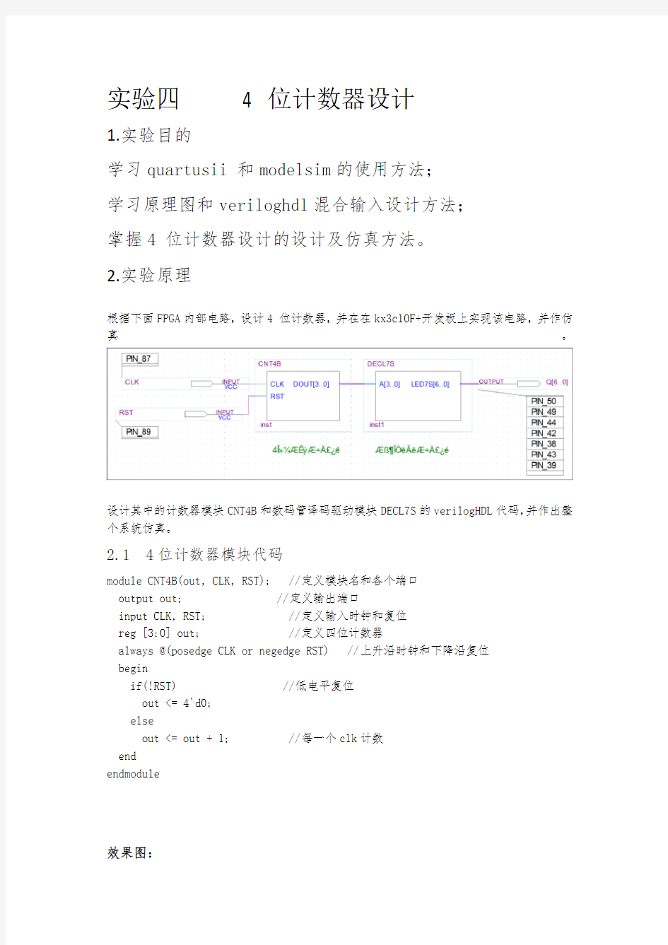
根据下面FPGA内部电路,设计4 位计数器,并在在kx3c10F+开发板上实现该电路,并作仿真。
设计其中的计数器模块CNT4B和数码管译码驱动模块DECL7S的verilogHDL代码,并作出整个系统仿真。
2.1 4位计数器模块代码
module CNT4B(out, CLK, RST); //定义模块名和各个端口
output out; //定义输出端口
input CLK, RST; //定义输入时钟和复位
reg [3:0] out; //定义四位计数器
always @(posedge CLK or negedge RST) //上升沿时钟和下降沿复位
begin
if(!RST) //低电平复位
out <= 4'd0;
else
out <= out + 1; //每一个clk计数
end
endmodule
效果图:
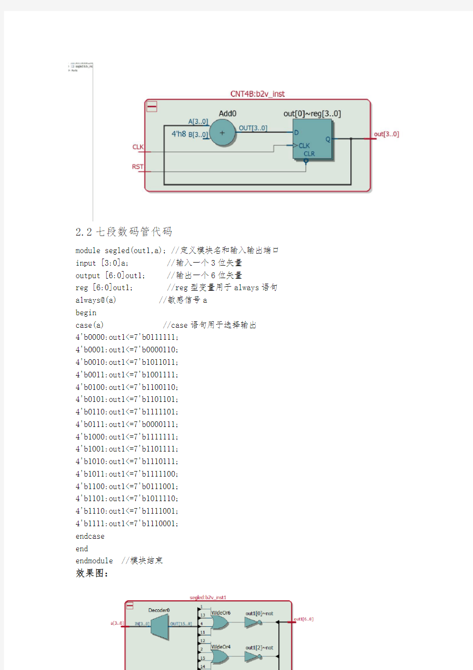
2.2七段数码管代码
module segled(out1,a); //定义模块名和输入输出端口input [3:0]a; //输入一个3位矢量
output [6:0]out1; //输出一个6位矢量
reg [6:0]out1; //reg型变量用于always语句always@(a) //敏感信号a
begin
case(a) //case语句用于选择输出
4'b0000:out1<=7'b0111111;
4'b0001:out1<=7'b0000110;
4'b0010:out1<=7'b1011011;
4'b0011:out1<=7'b1001111;
4'b0100:out1<=7'b1100110;
4'b0101:out1<=7'b1101101;
4'b0110:out1<=7'b1111101;
4'b0111:out1<=7'b0000111;
4'b1000:out1<=7'b1111111;
4'b1001:out1<=7'b1101111;
4'b1010:out1<=7'b1110111;
4'b1011:out1<=7'b1111100;
4'b1100:out1<=7'b0111001;
4'b1101:out1<=7'b1011110;
4'b1110:out1<=7'b1111001;
4'b1111:out1<=7'b1110001;
endcase
end
endmodule //模块结束
效果图:
2.3综合模块代码
// Copyright (C) 1991-2013 Altera Corporation
// Your use of Altera Corporation's design tools, logic functions // and other software and tools, and its AMPP partner logic
// functions, and any output files from any of the foregoing
// (including device programming or simulation files), and any
// associated documentation or information are expressly subject
// to the terms and conditions of the Altera Program License
// Subscription Agreement, Altera MegaCore Function License
// Agreement, or other applicable license agreement, including,
// without limitation, that your use is for the sole purpose of
// programming logic devices manufactured by Altera and sold by
// Altera or its authorized distributors. Please refer to the
// applicable agreement for further details.
// PROGRAM "Quartus II 64-Bit"
// VERSION "Version 13.1.0 Build 162 10/23/2013 SJ Web Edition" // CREATED "Tue Apr 11 22:35:09 2017"
module cou(
CLK,
RST,
Q
);
input wire CLK;
input wire RST;
output wire [6:0] Q;
wire [3:0] SYNTHESIZED_WIRE_0;
CNT4B b2v_inst(
.CLK(CLK),
.RST(RST),
.out(SYNTHESIZED_WIRE_0));
segled b2v_inst1(
.a(SYNTHESIZED_WIRE_0),
.out1(Q));
endmodule
效果图:
3.实验设备
kx3c10F+开发板,电脑。
4.实验步骤
4.1编译
4.1.1编译结果如下图所示:
编译解释:
在这个报告中,我们可以看到如下信息:
Total logic elements 11/5136(<1%): 该芯片中共有5136个LE资源,其中的11个在这个工程的这次编译中得到了使用。
Total combinational functions 11/5136(<1%): 该芯片的5136个LE资源中,其中11个用于实现组合逻辑。
Dedicated logic registers 4/5136(0%): 该芯片的5136个LE资源中,其中4个用于实现寄存器,即时序逻辑。
从上述信息中,可以得到组合逻辑与时序逻辑的使用比例——11/4= 2.75:1。
4.1.2综合出来的电路图