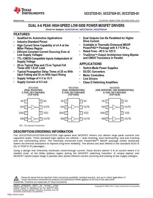
VDD OUTA NC OUTBNC – No internal connectionUCC27323(DUAL INVERTING)D,DGN,OR P PACKAGE(TOP VIEW)VDD OUTA NC OUTBUCC27324(DUAL NONINVERTING)D,DGN,OR P PACKAGE(TOP VIEW)VDD OUTANC OUTBUCC27325(ONE INVERTING,ONE )D,DGN,OR P PACKAGE(TOP VIEW)NONINVERTING UCC27323-Q1,UCC27324-Q1,UCC27325-Q1SLUS678A –MARCH 2008–REVISED APRIL 2012DUAL 4-A PEAK HIGH-SPEED LOW-SIDE POWER MOSFET DRIVERSCheck for Samples:UCC27323-Q1,UCC27324-Q1,UCC27325-Q1FEATURES•Qualified for Automotive Applications •Dual Outputs Can Be Paralleled for Higher Drive Current•Industry-Standard Pinout•Available in Thermally Enhanced MSOP •High Current Drive Capability of ±4A at the PowerPAD™Package with 4.7°C/W θJC Miller Plateau Region•Rated From –40°C to 125°C•Efficient Constant Current Sourcing Even at Low Supply Voltages•TrueDrive™Output Architecture Using Bipolar and CMOS Transistors in Parallel•TTL-/CMOS-Compatible Inputs Independent of Supply VoltageAPPLICATIONS•20-ns Typical Rise and 15-ns Typical Fall •Switch-Mode Power Supplies Times with 1.8-nF Load•DC/DC Converters •Typical Propagation Delay Times of 25ns With Input Falling and 35ns With Input Rising •Motor Controllers •Supply Voltage of 4V to 15V •Line Drivers•Supply Current of 0.3mA•Class D Switching AmplifiersDESCRIPTION/ORDERING INFORMATIONThe UCC27323/UCC27324/UCC27325high-speed dual MOSFET drivers can deliver large peak currents into capacitive loads.Three standard logic options are offered —dual inverting,dual noninverting,and one inverting and one noninverting driver.The thermally enhanced 8-pin PowerPAD™MSOP package (DGN)drastically lowers the thermal resistance to improve long-term reliability.The drivers are also offered in the standard SOIC-8(D)or PDIP-8(P)packages.Using a design that inherently minimizes shoot-through current,these drivers deliver 4A of current where it is needed most,at the Miller plateau region during the MOSFET switching transition.A unique bipolar and MOSFET hybrid output stage in parallel also allows efficient current sourcing and sinking at low supply voltages.Please be aware that an important notice concerning availability,standard warranty,and use in critical applications of Texas Instruments semiconductor products and disclaimers thereto appears at the end of this data sheet.PowerPAD,TrueDrive are trademarks of Texas Instruments.NCOUTAVDDOUTBINBGNDINA NCUCC27323-Q1,UCC27324-Q1,UCC27325-Q1SLUS678A –MARCH 2008–REVISED APRIL 2012ORDERING INFORMATION (1)OUTPUTORDERABLE TOP-SIDE T A =T JPACKAGE (2)CONFIGURATION PART NUMBERMARKING PowerPAD –DGNReel of 2000UCC27323QDGNRQ1PREVIEW Dual invertingPDIP –P Tube of 1000UCC27323QPQ1PREVIEW SOIC –D Reel of 2500UCC27323QDRQ1PREVIEW PowerPAD –DGNReel of 2000UCC27324QDGNRQ1PREVIEW –40°C to 125°CDual noninvertingPDIP –P Tube of 1000UCC27324QPQ1PREVIEW SOIC –D Reel of 2500UCC27324QDRQ127324Q PowerPAD –DGNReel of 2000UCC27325QDGNRQ1PREVIEW One inverting,PDIP –P Tube of 1000UCC27325QPQ1PREVIEW One noninvertingSOIC –DReel of 2500UCC27325QDRQ1PREVIEW(1)For the most current package and ordering information,see the Package Option Addendum at the end of this document,or see the TI web site at .(2)Package drawings,thermal data,and symbolization are available at /packaging .BLOCK DIAGRAMUCC27323-Q1,UCC27324-Q1,UCC27325-Q1 SLUS678A–MARCH2008–REVISED APRIL2012TERMINAL FUNCTIONSTERMINALI/O DESCRIPTION1NC No connection.Should be grounded.Input A.Input signal of the A driver.Has logic-compatible threshold and hysteresis.If not used,this input 2INA Ishould be tied to either V DD or GND.It should not be left floating.Common ground.Should be connected very closely to the source of the power MOSFET that the driver 3GNDis driving.Input B.Input signal of the A driver.Has logic-compatible threshold and hysteresis.If not used,this input 4INB Ishould be tied to either V DD or GND.It should not be left floating.5OUTB O Driver output B.The output stage can provide4-A drive current to the gate of a power MOSFET.6VDD I Supply.Supply voltage and the power input connection for this device.7OUTA O Driver output A.The output stage can provide4-A drive current to the gate of a power MOSFET.8NC No connection.Should be grounded.Table1.FUNCTION TABLEUCC27323UCC27324UCC27325 INPUTSOUTPUTS OUTPUTS OUTPUTS INA INB OUTA OUTB OUTA OUTB OUTA OUTB L L H H L L H LL H H L L H H HH L L H H L L LH H L L H H L HUCC27323-Q1,UCC27324-Q1,UCC27325-Q1SLUS678A–MARCH2008–REVISED ABSOLUTE MAXIMUM RATINGS(1)(2)over operating free-air temperature range(unless otherwise noted)V DD Supply voltage–0.3V to16VDC,I OUT_DC0.3AI O Output current(OUTA,OUTB)Pulsed(0.5μs),I OUT_PULSED 4.5ADGN package3WP D Power dissipation at T A=25°C D package650mWP package350mWT J Junction operating temperature–55°C to150°CT stg Storage temperature–65°C to150°CT lead Lead temperature Soldering,10s300°C(1)Stresses beyond those listed under absolute maximum ratings may cause permanent damage to the device.These are stress ratingsonly,and functional operation of the device at these or any other conditions beyond those indicated under recommended operating conditions is not implied.Exposure to absolute-maximum-rated conditions for extended periods may affect device reliability.(2)All voltages are with respect to GND.Currents are positive into and negative out of the specified terminal.POWER DISSIPATION RATINGSPOWER RATING(1)DERATING FACTOR(1) PACKAGEθJC(°C/W)θJA(°C/W)T A=70°C T A>70°C(mW)(mW/°C) D(SOIC-8)4284to160(2)344to655(2) 6.25to11.9(2)P(PDIP-8)491105009DGN(MSOP-84.750to59(2)1370(4)17.1(4)PowerPAD)(3)(1)125°C operating junction temperature is used for power rating calculations.(2)The range of values indicates the effect of the PC board.These values are intended to give the system designer an indication of thebest and worst case conditions.In general,the system designer should attempt to use larger traces on the PC board where possible to spread the heat away form the device more effectively.For information on the PowerPAD package,see the technical brief,PowerPad™Thermally Enhanced Package,Texas Instruments literature number SLMA002and the application brief,PowerPad™Made Easy,Texas Instruments literature number SLMA004.(3)The PowerPAD thermal pad is not directly connected to any leads of the package.However,it is electrically and thermally connected tothe substrate,which is the ground of the device.(4)150°C operating junction temperature is used for power rating calculations.OVERALL ELECTRICAL CHARACTERISTICSV CC=4.5V to15V,T A=–40°C to125°C(unless otherwise noted),T A=T JPARAMETER TEST CONDITIONS MIN TYP MAX UNITINB=0V300450INA=0VINB=HIGH300450UCC27323INB=0V300450INA=HIGHINB=HIGH300450INB=0V280INA=0VINB=HIGH300450I DD Static operating current UCC27324μAINB=0V300450INA=HIGHINB=HIGH600800INB=0V150300INA=0VINB=HIGH450600UCC27325INB=0V150300INA=HIGHINB=HIGH450600+5V16V0V0VUCC27323-Q1,UCC27324-Q1,UCC27325-Q1SLUS678A –MARCH 2008–REVISED APRIL 2012INPUT (INA,INB)ELECTRICAL CHARACTERISTICSV CC =4.5V to 15V,T A =–40°C to 125°C (unless otherwise noted)PARAMETERTEST CONDITIONSMIN TYPMAXUNIT V IH Logic 1input threshold 2V V ILLogic 0input threshold 1V Input current0V ≤V IN ≤V DD–1010μAOUTPUT (OUTA,OUTB)ELECTRICAL CHARACTERISTICSV CC =4.5V to 15V,T A =–40°C to 125°C (unless otherwise noted)PARAMETER TEST CONDITIONST AMIN TYP MAX UNIT Output current (1)(2)V DD =14V4A V OH High-level output voltage V OH =V DD –V OUT,I OUT =–10mA 300450mV V OLLow-level output level I OUT =10mA2245mV 25°C 253035Output resistance high (3)I OUT =–10mA,V DD =14V ΩFull range 184325°C 1.9 2.22.5Output resistance low (3)I OUT =10mA,V DD =14VΩFull range0.94Latch-up protection (1)500mA(1)Specified by design(2)The pullup/pulldown circuits of the driver are bipolar and MOSFET transistors in parallel.The pulsed output current rating is the combined current from the bipolar and MOSFET transistors.(3)The pullup/pulldown circuits of the driver are bipolar and MOSFET transistors in parallel.The output resistance is the R DS(ON)of the MOSFET transistor when the voltage on the driver output is less than the saturation voltage of the bipolar transistor.SWITCHING CHARACTERISTICSV CC =4.5V to 15V,T A =–40°C to 125°C (unless otherwise noted)(see Figure 1)PARAMETERTEST CONDITIONSMINTYP MAX UNIT t R Rise time (OUTA,OUTB)C LOAD =1.8nF 2040ns t F Fall time (OUTA,OUTB)C LOAD =1.8nF 1540ns t D1Delay time,IN rising (IN to OUT)C LOAD =1.8nF 2540ns t D2Delay time,IN falling (IN to OUT)C LOAD =1.8nF3550nsFigure 1.Switching Waveforms for (a)Inverting Driver and (b)Noninverting DriverUCC27323-Q1,UCC27324-Q1,UCC27325-Q1SLUS678A–MARCH2008–REVISED APPLICATION INFORMATIONGeneral InformationHigh-frequency power supplies often require high-speed high-current drivers such as those available in the UCC2732x family.A leading application is the need to provide a high-power buffer stage between the PWM output of the control device and the gates of the primary power MOSFET or IGBT switching devices.In other cases,the driver is used to drive the power device gates through a drive transformer.Synchronous rectification supplies also have the need to simultaneously drive multiple devices,which can present an extremely large load to the control circuitry.Drivers are used when it is not feasible to have the primary PWM regulator directly drive the switching devices for one or more reasons.The PWM device may not have the brute drive capability required for the intended switching MOSFET,limiting the switching performance in the application.In other cases,there may be a desire to minimize the effect of high-frequency switching noise by placing the high-current driver physically close to the load.Also,newer devices that target the highest operating frequencies may not incorporate onboard gate drivers at all.Their PWM outputs are intended to drive only the high-impedance input to a driver such as the UCC2732x. Finally,the control device may be under thermal stress due to power dissipation,and an external driver can help by moving the heat from the controller to an external package.Input StageThe input thresholds have a3.3-V logic sensitivity over the full range of V DD voltage,yet it is equally compatable with0V to V DD signals.The inputs of UCC2732x family of drivers are designed to withstand500-mA reverse current without damage to the device or logic upset.The input stage of each driver should be driven by a signal with a short rise or fall time. This condition is satisfied in typical power-supply applications,where the input signals are provided by a PWM controller or logic gates with fast transition times(<200ns).The input stages to the drivers function as a digital gate,and they are not intended for applications where a slow changing input voltage is used to generate a switching output when the logic threshold of the input section is reached.While this may not be harmful to the driver,the output of the driver may switch repeatedly at a high frequency.Users should not attempt to shape the input signals to the driver in an attempt to slow down(or delay)the signal at the output.If limiting the rise or fall times to the power device is desired,limit the rise or fall times to the power device,then an external resistance can be added between the output of the driver and the load device,which is generally a power MOSFET gate.The external resistor also may help remove power dissipation from the device package,as discussed in the Thermal Considerations section.Output StageInverting outputs of the UCC27323and OUTA of the UCC27325are intended to drive external P-channel MOSFETs.Noninverting outputs of the UCC27324and OUTB of the UCC27325are intended to drive external N-channel MOSFETs.Each output stage is capable of supplying±4-A peak current pulses and swings to both V DD and GND.The pullup/pulldown circuits of the driver are constructed of bipolar and MOSFET transistors in parallel.The peak output current rating is the combined current from the bipolar and MOSFET transistors.The output resistance is the R DS(ON)of the MOSFET transistor when the voltage on the driver output is less than the saturation voltage of the bipolar transistor.Each output stage also provides a very low impedance to overshoot and undershoot,due to the body diode of the external MOSFET.This means that,in many cases,external Schottky-clamp diodes are not required.The UCC27323family delivers a4-A gate drive when it is most needed during the MOSFET switching transition—at the Miller plateau region—providing improved efficiency gains.A unique bipolar and MOSFET hybrid output stage in parallel also allows efficient current sourcing at low supply voltages.V V 5.5VSUPPLY D 4.5 VADJ V UCC27323-Q1,UCC27324-Q1,UCC27325-Q1SLUS678A –MARCH 2008–REVISED APRIL 2012Source/Sink Capabilities During Miller PlateauLarge power MOSFETs present a large load to the control circuitry.Proper drive is required for efficient,reliable operation.The UCC2732x drivers have been optimized to provide maximum drive to a power MOSFET during the Miller plateau region of the switching transition.This interval occurs while the drain voltage is swinging between the voltage levels dictated by the power topology,requiring the charging/discharging of the drain-gate capacitance with current supplied or removed by the driver.[1]Two circuits are used to test the current capabilities of the UCC27323driver.In each case,external circuitry is added to clamp the output near 5V while the device is sinking or sourcing current.An input pulse of 250ns is applied at a frequency of 1kHz in the proper polarity for the respective test.In each test,there is a transient period when the current peaked up and then settled down to a steady-state value.The noted current measurements are made at a time of 200ns after the input pulse is applied,after the initial transient.The circuit in Figure 2is used to verify the current sink capability when the output of the driver is clamped at approximately 5V,a typical value of gate-source voltage during the Miller plateau region.The UCC27323is found to sink 4.5A at V DD =15V and 4.28A at V DD =12V.Figure 2.The circuit in Figure 3is used to test the current source capability with the output clamped to approximately 5V with a string of Zener diodes.The UCC27323is found to source 4.8A at V DD =15V and 3.7A at V DD =12V.Figure 3.C LOADUCC27323-Q1,UCC27324-Q1,UCC27325-Q1SLUS678A –MARCH 2008–REVISED APRIL 2012It should be noted that the current-sink capability is slightly stronger than the current source capability at lower V DD .This is due to the differences in the structure of the bipolar-MOSFET power output section,where the current source is a P-channel MOSFET and the current sink has an N-channel MOSFET.In a large majority of applications,it is advantageous that the turn-off capability of a driver is stronger than the turn-on capability.This helps to ensure that the MOSFET is held off during common power-supply transients that may turn the device back on.Parallel OutputsThe A and B drivers may be combined into a single driver by connecting the INA/INB inputs together and the OUTA/OUTB outputs together.Then,a single signal can control the paralleled combination as shown in Figure 4.Figure 4.Operational Waveforms and Circuit LayoutFigure 5shows the circuit performance achievable with a single driver (half of the 8-pin device)driving a 10-nF load.The input pulse width (not shown)is set to 300ns to show both transitions in the output waveform.Note the linear rise and fall edges of the switching waveforms.This is due to the constant output current characteristic of the driver as opposed to the resistive output impedance of traditional MOSFET-based gate drivers.Sink and source currents of the driver are dependent upon the VDD value and the output capacitive load.The larger the VDD value the higher the current capability,and the larger the capacitive load the higher the current sink/source capability.Trace resistance and inductance,including wires and cables for testing,slows down the rise and fall times of the outputs which reduces the current capabilities of the driver.To achieve higher current results,reduce resistance and inductance on the board as much as possible and increase the capacitive output load value in order to swap out the effect of the inductance values.UCC27323-Q1,UCC27324-Q1,UCC27325-Q1 SLUS678A–MARCH2008–REVISED APRIL2012Figure5.In a power driver operating at high frequency,it is a significant challenge to get clean waveforms without much overshoot/undershoot and ringing.The low output impedance of these drivers produces waveforms with high Δi/Δt.This tends to induce ringing in the parasitic inductances.Utmost care must be used in the circuit layout.It is advantageous to connect the driver as close as possible to the leads.The driver layout has ground on the opposite side of the output,so the ground should be connected to the bypass capacitors and the load with copper trace as wide as possible.These connections also should be made with a small enclosed loop area to minimize the inductance.V DDAlthough quiescent V DD current is very low,total supply current is higher,depending on OUTA and OUTB current and the programmed oscillator frequency.Total V DD current is the sum of quiescent V DD current and the average OUT current.Knowing the operating frequency and the MOSFET gate charge(Q g),average OUT current can be calculated from:I OUT=Q g×fWhere f is frequencyFor the best high-speed circuit performance,two V DD bypass capacitors are recommended to prevent noise problems.The use of surface-mount components is highly recommended.A0.1-μF ceramic capacitor should be located closest to the V DD to ground connection.In addition,a larger capacitor(such as1-μF)with relatively low ESR should be connected in parallel,to help deliver the high current peaks to the load.The parallel combination of capacitors should present a low-impedance characteristic for the expected current levels in the driver application.Drive Current and Power RequirementsThe UCC2732x drivers are capable of delivering4A of current to a MOSFET gate for a period of several hundred nanoseconds.High peak current is required to quickly turn on the device.Then,to turn off the device, the driver is required to sink a similar amount of current to ground.This repeats at the operating frequency of the power device.A MOSFET is used in this discussion,because it is the most common type of switching device used in high-frequency power-conversion equipment.References1and2discuss the current required to drive a power MOSFET and other capacitive-input switching devices.Reference2includes information on the previous generation of bipolar gate drivers.When a driver is tested with a discrete capacitive load,it is a fairly simple matter to calculate the power that is required from the bias supply.The energy that must be transferred from the bias supply to charge the capacitor is given by:E=½CV2Where C is the load capacitor and V is the bias voltage feeding the driverUCC27323-Q1,UCC27324-Q1,UCC27325-Q1SLUS678A–MARCH2008–REVISED There is an equal amount of energy transferred to ground when the capacitor is discharged.This leads to apower loss given by:P=2×½CV2fWhere f is the switching frequencyThis power is dissipated in the resistive elements of the circuit.Thus,with no external resistor between the driver and gate,this power is dissipated inside the driver.Half of the total power is dissipated when the capacitor is charged,and the other half is dissipated when the capacitor is discharged.An actual example using the conditions of the previous gate drive waveform should help clarify this.With V DD=12V,C LOAD=10nF,and f=300kHz,the power loss can be calculated as:P=10nF×(12)2×(300kHz)=0.432WWith a12-V supply,this equates to a current of:I=P/V=0.432W/12V=0.036AThe actual current measured from the supply was0.037A,which is very close to the predicted value.But,theI DD current that is due to the internal consumption should be considered.With no load,the current draw is0.0027A.Under this condition,the output rise and fall times are faster than with a load.This could lead to an almost insignificant,yet measurable current due to cross-conduction in the output stages of the driver.However, these small current differences are buried in the high-frequency switching spikes and are beyond the measurement capabilities of a basic lab setup.The measured current with10-nF load is reasonably close to the expected value.The switching load presented by a power MOSFET can be converted to an equivalent capacitance by examining the gate charge required to switch the device.This gate charge includes the effects of the input capacitance plus the added charge needed to swing the drain of the device between the on and off states.Most manufacturers provide specifications that provide the typical and maximum gate charge,in nC,to switch the device under specified ing the gate charge Q g,one can determine the power that must be dissipated when charging a capacitor.This is done by using the equivalence Q g=CeffV to provide the following equation for power:P=C×V2×f=Q g×fThis equation allows a power designer to calculate the bias power required to drive a specific MOSFET gate at a specific bias voltage.Thermal InformationThe useful range of a driver is greatly affected by the drive power requirements of the load and the thermal characteristics of the package.For a power driver to be useful over a particular temperature range,the package must allow for the efficient removal of the heat produced while keeping the junction temperature within rated limits.The UCC2732x family of drivers is available in three different packages to cover a range of application requirements.As shown in Power Dissipation Ratings,the SOIC-8(D)and PDIP-8(P)packages have power ratings of approximately0.5W at T A=70°C.This limit is imposed in conjunction with the power derating factor also given in the table.Note that the power dissipation in our earlier example is0.432W with a10-nF load,12-V V DD, switched at300kHz.Thus,only one load of this size could be driven using the D or P package,even if the two onboard drivers are paralleled.The difficulties with heat removal limit the drive available in the older packages. The MSOP PowerPAD™package(DGN)significantly relieves this concern by offering an effective means of removing the heat from the semiconductor junction.As illustrated in Reference2,the PowerPAD packages offer a lead-frame die pad that is exposed at the base of the package.This pad is soldered to the copper on the PC board directly underneath the package,reducing theθJC to4.75°C/W.Data is presented in Reference2to show that the power dissipation can be quadrupled in the PowerPAD configuration when compared to the standard packages.The PC board must be designed with thermal lands and thermal vias to complete the heat removal subsystem,as summarized in Reference3.This allows a significant improvement in heatsink capability over that available in the D or P packages and is shown to more than double the power capability of the D and P packages.分销商库存信息: TIUCC27324QDRQ1。