UVI Alliance LD4&LD2产品技术资料
- 格式:pdf
- 大小:1.66 MB
- 文档页数:2


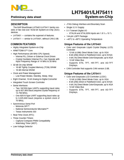
LH75401/LH75411 Preliminary data sheet System-on-ChipDESCRIPTIONThe NXP BlueStreak LH75401/LH75411 family con-sists of two low-cost 16/32-bit System-on-Chip (SoC) devices.•LH75401 — contains the superset of features.•LH75411 — similar to LH75401, without CAN 2.0B.COMMON FEATURES•Highly Integrated System-on-Chip•ARM7TDMI-S™ Core•High Performance (84 MHz CPU Speed)–Internal PLL Driven or External Clock Driven–Crystal Oscillator/Internal PLL Can Operate with Input Frequency Range of 14 MHz to 20MHz •32kB On-chip SRAM–16kB Tightly Coupled Memory (TCM) SRAM–16kB Internal SRAM•Clock and Power Management–Low Power Modes: Standby, Sleep, Stop •Eight Channel, 10-bit Analog-to-Digital Converter •Integrated Touch Screen Controller•Serial interfaces–Two 16C550-type UARTs supporting baud rates up to 921,600 baud (requires crystal frequency of14.756 MHz).–One 82510-type UART supporting baud rates up to 3,225,600 baud (requires a system clock of70MHz).•Synchronous Serial Port–Motorola SPI™–National Semiconductor Microwire™–Texas Instruments SSI•Real-Time Clock (RTC)•Three Counter/Timers–Capture/Compare/PWM Compatibility–Watchdog Timer (WDT)•Low-Voltage Detector •JTAG Debug Interface and Boundary Scan •Single 3.3 V Supply• 5 V Tolerant Digital I/O–XTALIN and XTAL32IN inputs are 1.8 V ± 10%•144-pin LQFP Package•−40°C to +85°C Operating TemperatureUnique Features of the LH75401•Color and Grayscale Liquid Crystal Display (LCD) Controller–12-bit (4,096) Direct Mode Color, up to VGA–8-bit (256) Direct or Palettized Color, up to SVGA –4-bit (16) Direct Mode Color/Grayscale, up to XGA –12-bit Video Bus–Supports STN, TF T, HR-TF T, and AD-TF T Displays.•CAN Controller that supports CAN version 2.0B.Unique Features of the LH75411•Color and Grayscale LCD Controller (LCDC)–12-bit (4,096) Direct Mode Color, up to VGA–8-bit (256) Direct or Palettized Color, up to SVGA –4-bit (16) Direct Mode Color/Grayscale, up to XGA –12-bit Video Bus–Supports STN, TF T, HR-TF T, and AD-TF T Displays.元器件交易网Preliminary data sheet 1LH75401/LH75411System-on-Chip2Rev. 01— 16 July 2007Preliminary data sheetNXP SemiconductorsORDERING INFORMATIONTable 1.Ordering informationType number PackageVersionName DescriptionLH75401N0Q100C0LQFP144plastic low profile quad flat package; 144 leads;body 20 x 20 x 1.4 mmSOT486-1LH75411N0Q100C0LQFP144plastic low profile quad flat package; 144 leads;body 20 x 20 x 1.4 mmSOT486-1元器件交易网System-on-ChipLH75401/LH75411Preliminary data sheet Rev. 01 — 16 July 2007 3NXP SemiconductorsLH75401 BLOCK DIAGRAMFigure 1.LH75401 Block Diagram元器件交易网LH75401/LH75411System-on-Chip4Rev. 01— 16 July 2007Preliminary data sheetNXP SemiconductorsLH75411 BLOCK DIAGRAMFigure 2.LH75411 Block Diagram元器件交易网System-on-ChipLH75401/LH75411Preliminary data sheet Rev. 01 — 16 July 2007 5NXP SemiconductorsPIN CONFIGURATIONFigure 3.LH75401/LH75411 pin configuration元器件交易网LH75401/LH75411System-on-Chip6Rev. 01— 16 July 2007Preliminary data sheetNXP SemiconductorsLH75401 Numerical Pin ListingTable 2.LH75401 Numerical Pin ListPIN NO.FUNCTION AT RESETFUNCTION2FUNCTION 3FUNCTION TYPE OUTPUTDRIVEBUFFERTYPE BEHAVIOR DURINGRESETNOTES 1PA7D15I/O 8 mA Bidirectional Pull-up 12PA6D14I/O 8 mA Bidirectional Pull-up 13VDD Power None 4PA5D13I/O 8 mA Bidirectional Pull-up 15PA4D12I/O 8 mA Bidirectional Pull-up 16PA3D11I/O 8 mA Bidirectional Pull-up 17PA2D10I/O 8 mA Bidirectional Pull-up 18VSS Ground None 9PA1D9I/O 8 mA Bidirectional Pull-up 110PA0D8I/O 8 mA Bidirectional Pull-up 111VDDC Power None 12D7I/O 8 mA Bidirectional Pull-up 13D6I/O 8 mA Bidirectional Pull-up 14VSSC Ground None 15D5I/O 8 mA Bidirectional Pull-up 16D4I/O 8 mA Bidirectional Pull-up 17VDD Power None 18D3I/O 8 mA Bidirectional Pull-up 19D2I/O 8 mA Bidirectional Pull-up 20D1I/O 8 mA Bidirectional Pull-up 21D0I/O8 mA Bidirectional Pull-up 22nWE 8 mA Output HIGH 323nOE 8 mA Output HIGH 324PB5nWAIT 8 mA Bidirectional Pull-up 1, 325PB4nBLE18 mA Bidirectional Pull-up 1, 326VSS GroundNone 27PB3nBLE08 mA Bidirectional Pull-up 1, 328PB2nCS38 mA Bidirectional Pull-up 1, 329PB1nCS28 mA Bidirectional Pull-up 1, 330PB0nCS18 mA Bidirectional Pull-up 1, 331nCS08 mA Output Pull-up 332PC7A238 mA Bidirectional Pull-down 133PC6A228 mA BidirectionalPull-down134VDD PowerNone 35PC5A218 mA Bidirectional Pull-down 136PC4A208 mA Bidirectional Pull-down 137PC3A198 mA Bidirectional Pull-down 138PC2A188 mABidirectionalPull-down1元器件交易网System-on-ChipLH75401/LH75411Preliminary data sheet Rev. 01 — 16 July 2007 7NXP Semiconductors39PC1A178 mA Bidirectional Pull-down 140PC0A168 mA BidirectionalPull-down141VSS Ground None 42VDD PowerNone 43A158 mA Output LOW 44A148 mA Output LOW 45A138 mA Output LOW 46A128 mA Output LOW 47A118 mA OutputLOW48VSS GroundNone 49A108 mA Output LOW 50A98 mA Output LOW 51A88 mA Output LOW 52A78 mA Output LOW 53A68 mA OutputLOW54VDD Power None 55A58 mA Output LOW 56A48 mA Output LOW 57A38 mA Output LOW 58A28 mA OutputLOW59VSS Ground None 60A18 mA Output LOW 61A08 mA Output LOW 62nRESETIN None Input Pull-up 2, 363TEST2None Input Pull-up 264TEST1None Input Pull-up 265TMS None Input Pull-up266RTCK 8 mA Output 67TCK None Input 68TDI None Input Pull-up269TDO 4 mA Output 70LINREGEN None Input 571nRESETOUT8 mA Output 372PD6INT6DREQ 6 mA Bidirectional Pull-down173PD5INT5DACK 6 mA Bidirectional 1, 274PD4INT4UARTRX18 mA BidirectionalPull-up 175VDDC Power None 76PD3INT3UARTTX18 mA Bidirectional Pull-up 177PD2INT2 2 mA Bidirectional Pull-up178PD1INT1 6 mA Bidirectional 1, 279PD0INT02 mA Bidirectional180VSSCGroundNoneTable 2.LH75401 Numerical Pin List (Cont’d)PIN NO.FUNCTION AT RESETFUNCTION2FUNCTION 3FUNCTION TYPE OUTPUTDRIVEBUFFERTYPE BEHAVIOR DURINGRESETNOTES 元器件交易网LH75401/LH75411System-on-Chip8Rev. 01— 16 July 2007Preliminary data sheetNXP Semiconductors81nPOR None Input Pull-up2, 382XTAL32IN None Input 483XTAL32OUT None Output84VSSA_PLL Ground None 85VDDA_PLL PowerNone 86XTALIN None Input 487XTALOUT None Output88VSSA_ADC Ground None 89AN3 (LR/Y-)PJ7None Input 90AN4 (Wiper)PJ6None Input 91AN9PJ5None Input 92AN2 (LL/Y+)PJ4None Input 93AN8PJ3None Input 94AN1 (UR/X-)PJ2None Input 95AN6PJ1None Input 96AN0 (UL/X+)PJ0None Input 97VDDA_ADCPower None 98VDD Power None 99PE7SSPFRM 4 mA Bidirectional Pull-up 1100PE6SSPCLK 4 mA Bidirectional Pull-down 1101PE5SSPRX 4 mA Bidirectional Pull-up 1102PE4SSPTX 4 mA Bidirectional Pull-down 1103PE3CANTX UARTTX08 mA Bidirectional Pull-up 1104PE2CANRX UARTRX02 mA Bidirectional Pull-up 1105PE1UARTTX24 mA BidirectionalPull-up1106VSS GroundNone 107PE0UARTRX2 4 mA Bidirectional Pull-up1108PF6CTCAP2B CTCMP2B 4 mA Bidirectional 2109PF5CTCAP2A CTCMP2A 4 mA Bidirectional 110PF4CTCAP1B CACMP1B 4 mA Bidirectional 2111PF3CTCAP1ACTCMP1A4 mA Bidirectional112VDD PowerNone 113PF2CTCAP0E 4 mA Bidirectional 2114PF1CTCAP0D 4 mA Bidirectional 115PF0CTCAP0C 4 mA Bidirectional 2116PG7CTCAP0B CTCMP0B 4 mA Bidirectional 117PG6CTCAP0A CTCMP0A4 mA Bidirectional 2118PG5CTCLK4 mA Bidirectional119VSS GroundNone 120PG4LCDVEEEN LCDMOD8 mA Bidirectional 121PG3LCDVDDEN 8 mA Bidirectional 122PG2LCDDSPLENLCDREV 8 mABidirectional Table 2.LH75401 Numerical Pin List (Cont’d)PIN NO.FUNCTION AT RESET FUNCTION2FUNCTION 3FUNCTION TYPE OUTPUTDRIVEBUFFERTYPE BEHAVIOR DURINGRESETNOTES 元器件交易网System-on-ChipLH75401/LH75411Preliminary data sheet Rev. 01 — 16 July 2007 9NXP SemiconductorsNOTES:1.Signal is selectable as pull-up, pull-down, or no pull-up/pull-down via the I/O Configuration peripheral.2.CMOS Schmitt trigger input.3.Signals preceded with ‘n’ are active LOW.4.Crystal Oscillator Inputs should be driven to 1.8 V ±10% (MAX.)5.LINREGEN activation requires a 0 Ω pull-up to VDD.123PG1LCDCLS 8 mA Bidirectional 124PG0LCDPS 8 mA Bidirectional 125PH7LCDDCLK8 mABidirectional126VDD Power None 127VSS GroundNone 128PH6LCDLP LCDHRLP 8 mA Bidirectional 129PH5LCDFP LCDSPS 8 mA Bidirectional 130PH4LCDEN LCDSPL8 mA Bidirectional 131PH3LCDVD118 mA Bidirectional 132PH2LCDVD108 mA Bidirectional 133PH1LCDVD98 mABidirectional 134VDD PowerNone 135PH0LCDVD88 mA Bidirectional 136PI7LCDVD78 mA Bidirectional 137PI6LCDVD68 mA Bidirectional 138PI5LCDVD58 mA Bidirectional 139PI4LCDVD48 mABidirectional 140VSS GroundNone 141PI3LCDVD38 mA Bidirectional 142PI2LCDVD28 mA Bidirectional 143PI1LCDVD18 mA Bidirectional 144PI0LCDVD08 mABidirectionalTable 2.LH75401 Numerical Pin List (Cont’d)PIN NO.FUNCTION AT RESETFUNCTION2FUNCTION 3FUNCTION TYPE OUTPUTDRIVEBUFFERTYPE BEHAVIOR DURINGRESETNOTESLH75401/LH75411System-on-Chip10Rev. 01 — 16 July 2007Preliminary data sheetNXP SemiconductorsLH75401 Signal DescriptionsTable 3.LH75401 Signal DescriptionsPIN NO.SIGNAL NAMETYPEDESCRIPTIONNOTESMEMORY INTERFACE (MI)1245679101213151618192021D[15:0]Input/Output Data Input/Output Signals 122nWE Output Static Memory Controller Write Enable 223nOE Output Static Memory Controller Output Enable 224nWAIT Input Static Memory Controller External Wait Control 1, 225nBLE1Output Static Memory Controller Byte Lane Strobe 1, 227nBLE0Output Static Memory Controller Byte Lane Strobe 1, 228nCS3Output Static Memory Controller Chip Select 1, 229nCS2Output Static Memory Controller Chip Select 1, 230nCS1Output Static Memory Controller Chip Select 1, 231nCS0OutputStatic Memory Controller Chip Select23233 35363738394043444546474950515253555657586061A[23:0]Output Address Signals 1DMA CONTROLLER (DMAC)72DREQ Input DMA Request 173DACKOutputDMA Acknowledge1PIN NO.SIGNAL NAME TYPE DESCRIPTION NOTESCOLOR LCD CONTROLLER (CLCDC)120LCDMOD Output Signal Used by the Row Driver (AD-TFT, HR-TFT only)1 120LCDVEEEN Output Analog Supply Enable (AC Bias SIgnal)1 121LCDVDDEN Output Digital Supply Enable1 122LCDDSPLEN Output LCD Panel Power Enable1 122LCDREV Output Reverse Signal (AD-TFT, HR-TFT only)1 123LCDCLS Output Clock to the Row Drivers (AD-TFT, HR-TFT only)1 124LCDPS Output Power Save (AD-TFT, HR-TFT only)1 125LCDDCLK Output LCD Panel Clock1 128LCDLP Output Line Synchronization Pulse (STN), Horizontal Synchronization Pulse (TFT)1 128LCDHRLP Output Latch Pulse (AD-TFT, HR-TFT only)1 129LCDFP Output Frame Pulse (STN), Vertical Synchronization Pulse (TFT)1 129LCDSPS Output Row Driver Counter Reset Signal (AD-TFT, HR-TFT only)1 130LCDEN Output LCD Data Enable1 130LCDSPL Output Start Pulse Left (AD-TFT, HR-TFT only)1 131132133135136137LCDVD[11:0]Output LCD Panel Data bus1 138139141142143144SYNCHRONOUS SERIAL PORT (SSP)99SSPFRM Output SSP Serial Frame1 100SSPCLK Output SSP Clock1 101SSPRX Input SSP RXD1 102SSPTX Output SSP TXD1UART0 (U0)103UARTTX0Output UART0 Transmitted Serial Data Output1 104UARTRX0Input UART0 Received Serial Data Input1UART1 (U1)74UARTRX1Input UART1 Received Serial Data Input1 76UARTTX1Output UART1 Transmitted Serial Data Output1UART2 (U2)105UARTTX2Output UART2 Transmitted Serial Data Output1 107UARTRX2Input UART2 Received Serial Data Input1CONTROLLER AREA NETWORK (CAN)103CANTX Output CAN Transmitted Serial Data Output1 104CANRX Input CAN Received Serial Data Input1ANALOG-TO-DIGITAL CONVERTER (ADC)89 90 91 92 93 94 95 96AN3 (LR/Y-)AN4 (Wiper)AN9AN2 (LL/Y+)AN8AN1 (UR/X-)AN6AN0 (UL/X+)Input ADC Inputs1TIMER 0117116115114113CTCAP0[A:E]Input Timer 0 Capture Inputs1117116CTCMP0[A:B]Output Timer 0 Compare Outputs1 118CTCLK Input Common External Clock1TIMER 1111110CTCAP1[A:B]Input Timer 1 Capture Inputs1 111110CTCMP1[A:B]Output Timer 1 Compare Outputs1 118CTCLK Input Common External Clock1TIMER 2109108CTCAP2[A:B]Input Timer 2 Capture Inputs1 109108CTCMP2[A:B]Input Timer 2 Compare Outputs1 118CTCLK Input Common External Clock1GENERAL PURPOSE INPUT/OUTPUT (GPIO)1 2 4 5 6 7 9 10PA7PA6PA5PA4PA3PA2PA1PA0Input/Output General Purpose I/O Signals - Port A124 25 27 28 29 30PB5PB4PB3PB2PB1PB0Input/Output General Purpose I/O Signals - Port B132 33 35 36 37 38 39 40PC7PC6PC5PC4PC3PC2PC1PC0Input/Output General Purpose I/O Signals - Port C1PIN NO.SIGNAL NAME TYPE DESCRIPTION NOTES72 73 74 76 77 78 79PD6PD5PD4PD3PD2PD1PD0Input/Output General Purpose I/O Signals - Port D189 90 91 92 93 94 95 96PJ7PJ6PJ5PJ4PJ3PJ2PJ1PJ0Input General Purpose I/O Signals - Port J199 100 101 102 103 104 105 107PE7PE6PE5PE4PE3PE2PE1PE0Input/Output General Purpose I/O Signals - Port E1108 109 110 111 113 114 115PF6PF5PF4PF3PF2PF1PF0Input/Output General Purpose I/O Signals - Port F1116 117 118 120 121 122 123 124PG7PG6PG5PG4PG3PG2PG1PG0Input/Output General Purpose I/O Signals - Port G1125 128 129 130 131 132 133 135PH7PH6PH5PH4PH3PH2PH1PH0Input/Output General Purpose I/O Signals - Port H1136 137 138 139 141 142 143 144PI7PI6PI5PI4PI3PI2PI1PI0Input/Output General Purpose I/O Signals - Port I1 RESET, CLOCK, AND POWER CONTROLLER (RCPC)62nRESETIN Input User Reset Input2 71nRESETOUT Output System Reset Output2 72INT6Input External Interrupt Input 61 PIN NO.SIGNAL NAME TYPE DESCRIPTION NOTESNOTES:1.These pin numbers have multiplexed functions.2.Signals preceded with ‘n’ are active LOW.73INT5Input External Interrupt Input 5174INT4Input External Interrupt Input 4176INT3Input External Interrupt Input 3177INT2Input External Interrupt Input 2178INT1Input External Interrupt Input 1179INT0Input External Interrupt Input 0181nPOR Input Power-on Reset Input282XTAL32IN Input 32.768 kHz Crystal Clock Input 83XTAL32OUT Output 32.768 kHz Crystal Clock Output 86XTALIN Input Crystal Clock Input 87XTALOUT Output Crystal Clock OutputTEST INTERFACE63TEST2Input Test Mode Pin 264TEST1Input Test Mode Pin 165TMS Input JTAG Test Mode Select Input 66RTCK Output Returned JTAG Test Clock Output 67TCK Input JTAG Test Clock Input 68TDI Input JTAG Test Serial Data Input 69TDOOutputJTAG Test Data Serial OutputPOWER AND GROUND (GND)31734425498112126134VDD Power I/O Ring VDD826414859106119127140VSS Power I/O Ring VSS1175VDDC Power Core VDD supply (Output if Linear Regulator Enabled, Otherwise Input)1480VSSC Power Core VSS70LINREGEN Input Linear Regulator Enable 84VSSA_PLL Power PLL Analog VSS 85VDDA_PLL Power PLL Analog VDD Supply 88VSSA_ADC Power A-to-D converter Analog VSS 97VDDA_ADCPowerA-to-D converter Analog VDD SupplyPIN NO.SIGNAL NAME TYPE DESCRIPTIONNOTESLH75411 Numerical Pin ListingTable 4.LH75411 Numerical Pin ListPIN NO.FUNCTIONAT RESETFUNCTION2FUNCTION3FUNCTIONTYPEOUTPUTDRIVEBUFFERTYPEBEHAVIOR DURINGRESET NOTES1PA7D15I/O8 mA Bidirectional Pull-up1 2PA6D14I/O8 mA Bidirectional Pull-up1 3VDD Power None4PA5D13I/O8 mA Bidirectional Pull-up1 5PA4D12I/O8 mA Bidirectional Pull-up1 6PA3D11I/O8 mA Bidirectional Pull-up1 7PA2D10I/O8 mA Bidirectional Pull-up1 8VSS Ground None9PA1D9I/O8 mA Bidirectional Pull-up1 10PA0D8I/O8 mA Bidirectional Pull-up1 11VDDC Power None12D7I/O8 mA Bidirectional Pull-up13D6I/O8 mA Bidirectional Pull-up14VSSC Ground None15D5I/O8 mA Bidirectional Pull-up16D4I/O8 mA Bidirectional Pull-up17VDD Power None18D3I/O8 mA Bidirectional Pull-up19D2I/O8 mA Bidirectional Pull-up20D1I/O8 mA Bidirectional Pull-up21D0I/O8 mA Bidirectional Pull-up22nWE8 mA Output HIGH3 23nOE8 mA Output HIGH3 24PB5nWAIT8 mA Bidirectional Pull-up1, 3 25PB4nBLE18 mA Bidirectional Pull-up1, 3 26VSS Ground None27PB3nBLE08 mA Bidirectional Pull-up1, 3 28PB2nCS38 mA Bidirectional Pull-up1, 3 29PB1nCS28 mA Bidirectional Pull-up1, 3 30PB0nCS18 mA Bidirectional Pull-up1, 3 31nCS08 mA Output Pull-up3 32PC7A238 mA Bidirectional Pull-down1 33PC6A228 mA Bidirectional Pull-down1 34VDD Power None35PC5A218 mA Bidirectional Pull-down1 36PC4A208 mA Bidirectional Pull-down1 37PC3A198 mA Bidirectional Pull-down1 38PC2A188 mA Bidirectional Pull-down1 39PC1A178 mA Bidirectional Pull-down1 40PC0A168 mA Bidirectional Pull-down1 41VSS Ground None42VDD PowerNone 43A158 mA Output LOW 44A148 mA Output LOW 45A138 mA Output LOW 46A128 mA Output LOW 47A118 mA OutputLOW48VSS GroundNone 49A108 mA Output LOW 50A98 mA Output LOW 51A88 mA Output LOW 52A78 mA Output LOW 53A68 mA OutputLOW54VDD Power None 55A58 mA Output LOW 56A48 mA Output LOW 57A38 mA Output LOW 58A28 mA OutputLOW59VSS Ground None 60A18 mA Output LOW 61A08 mA Output LOW 62nRESETIN None Input Pull-up 2, 363TEST2None Input Pull-up 264TEST1None Input Pull-up 265TMS None Input Pull-up266RTCK 8 mA Output 67TCK None Input 68TDI None Input Pull-up269TDO 4 mA Output 70LINREGEN None Input 571nRESETOUT8 mA Output 372PD6INT6DREQ 6 mA Bidirectional Pull-down173PD5INT5DACK 6 mA Bidirectional 1, 274PD4INT4UARTRX18 mA BidirectionalPull-up 175VDDC Power None 76PD3INT3UARTTX18 mA Bidirectional Pull-up 177PD2INT2 2 mA Bidirectional Pull-up178PD1INT1 6 mA Bidirectional 1, 279PD0INT02 mA Bidirectional180VSSC GroundNone 81nPOR None Input Pull-up2, 382XTAL32IN None Input 483XTAL32OUTNoneOutputPIN NO.FUNCTION AT RESETFUNCTION2FUNCTION 3FUNCTION TYPE OUTPUTDRIVEBUFFERTYPEBEHAVIOR DURINGRESETNOTES84VSSA_PLL Ground None 85VDDA_PLL PowerNone 86XTALIN None Input 487XTALOUT None Output88VSSA_ADC GroundNone 89AN3 (LR/Y-)PJ7None Input 90AN4 (Wiper)PJ6None Input 91AN9PJ5None Input 92AN2 (LL/Y+)PJ4None Input 93AN8PJ3None Input 94AN1 (UR/X-)PJ2None Input 95AN6PJ1None Input 96AN0 (UL/X+)PJ0None Input 97VDDA_ADCPower None 98VDD Power None 99PE7SSPFRM 4 mA Bidirectional Pull-up 1100PE6SSPCLK 4 mA Bidirectional Pull-down 1101PE5SSPRX 4 mA Bidirectional Pull-up 1102PE4SSPTX 4 mA Bidirectional Pull-down 1103PE3UARTTX08 mA Bidirectional Pull-up 1104PE2UARTRX0 2 mA Bidirectional Pull-up 1105PE1UARTTX24 mA BidirectionalPull-up1106VSS GroundNone 107PE0UARTRX2 4 mA Bidirectional Pull-up1108PF6CTCAP2B CTCMP2B 4 mA Bidirectional 2109PF5CTCAP2A CTCMP2A 4 mA Bidirectional 110PF4CTCAP1B CACMP1B 4 mA Bidirectional 2111PF3CTCAP1ACTCMP1A4 mA Bidirectional112VDD PowerNone 113PF2CTCAP0E 4 mA Bidirectional 2114PF1CTCAP0D 4 mA Bidirectional 115PF0CTCAP0C 4 mA Bidirectional 2116PG7CTCAP0B CTCMP0B 4 mA Bidirectional 117PG6CTCAP0A CTCMP0A4 mA Bidirectional 2118PG5CTCLK4 mA Bidirectional119VSS GroundNone 120PG4LCDVEEEN LCDMOD8 mA Bidirectional 121PG3LCDVDDEN 8 mA Bidirectional 122PG2LCDDSPLEN LCDREV 8 mA Bidirectional 123PG1LCDCLS 8 mA Bidirectional 124PG0LCDPS 8 mA Bidirectional 125PH7LCDDCLK8 mABidirectional PIN NO.FUNCTION AT RESET FUNCTION2FUNCTION 3FUNCTION TYPE OUTPUTDRIVEBUFFERTYPEBEHAVIOR DURINGRESETNOTESNOTES:1.Signal is selectable as pull-up, pull-down, or no pull-up/pull-down via the I/O Configuration peripheral.2.CMOS Schmitt trigger input.3.Signals preceded with ‘n’ are active LOW.4.Crystal Oscillator Inputs should be driven to 1.8 V ±10% (MAX.)5.LINREGEN activation requires a 0 Ω pull-up to VDD.126VDD Power None 127VSS GroundNone 128PH6LCDLP LCDHRLP 8 mA Bidirectional 129PH5LCDFP LCDSPS 8 mA Bidirectional 130PH4LCDEN LCDSPL8 mA Bidirectional 131PH3LCDVD118 mA Bidirectional 132PH2LCDVD108 mA Bidirectional 133PH1LCDVD98 mABidirectional 134VDD PowerNone 135PH0LCDVD88 mA Bidirectional 136PI7LCDVD78 mA Bidirectional 137PI6LCDVD68 mA Bidirectional 138PI5LCDVD58 mA Bidirectional 139PI4LCDVD48 mABidirectional 140VSS GroundNone 141PI3LCDVD38 mA Bidirectional 142PI2LCDVD28 mA Bidirectional 143PI1LCDVD18 mA Bidirectional 144PI0LCDVD08 mABidirectionalPIN NO.FUNCTION AT RESETFUNCTION2FUNCTION 3FUNCTION TYPE OUTPUTDRIVEBUFFERTYPE BEHAVIOR DURINGRESETNOTESLH75411 Signal DescriptionsTable 5.LH75411 Signal DescriptionsPIN NO.SIGNAL NAME TYPE DESCRIPTION NOTESMEMORY INTERFACE (MI)124567910D[15:0]Input/Output Data Input/Output Signals1 121315161819202122nWE Output Static Memory Controller Write Enable2 23nOE Output Static Memory Controller Output Enable2 24nWAIT Input Static Memory Controller External Wait Control1, 2 25nBLE1Output Static Memory Controller Byte Lane Strobe1, 2 27nBLE0Output Static Memory Controller Byte Lane Strobe1, 2 28nCS3Output Static Memory Controller Chip Select1, 2 29nCS2Output Static Memory Controller Chip Select1, 2 30nCS1Output Static Memory Controller Chip Select1, 2 31nCS0Output Static Memory Controller Chip Select2 323335363738394043444546A[23:0]Output Address Signals1 474950515253555657586061DMA CONTROLLER (DMAC)72DREQ Input DMA Request1 73DACK Output DMA Acknowledge1COLOR LCD CONTROLLER (CLCDC)120LCDMOD Output Signal Used by the Row Driver (AD-TFT, HR-TFT only)1 120LCDVEEEN Output Analog Supply Enable (AC Bias SIgnal)1 121LCDVDDEN Output Digital Supply Enable1 122LCDDSPLEN Output LCD Panel Power Enable1 122LCDREV Output Reverse Signal (AD-TFT, HR-TFT only)1 123LCDCLS Output Clock to the Row Drivers (AD-TFT, HR-TFT only)1 124LCDPS Output Power Save (AD-TFT, HR-TFT only)1 125LCDDCLK Output LCD Panel Clock1 128LCDLP Output Line Synchronization Pulse (STN), Horizontal Synchronization Pulse (TFT)1 128LCDHRLP Output Latch Pulse (AD-TFT, HR-TFT only)1 129LCDFP Output Frame Pulse (STN), Vertical Synchronization Pulse (TFT)1 129LCDSPS Output Row Driver Counter Reset Signal (AD-TFT, HR-TFT only)1 130LCDEN Output LCD Data Enable1 130LCDSPL Output Start Pulse Left (AD-TFT, HR-TFT only)1 131132133135136137138139141142143144LCDVD[11:0]Output LCD Panel Data bus1SYNCHRONOUS SERIAL PORT (SSP)99SSPFRM Output SSP Serial Frame1 100SSPCLK Output SSP Clock1 101SSPRX Input SSP RXD1 102SSPTX Output SSP TXD1UART0 (U0)104UARTRX0Input UART0 Received Serial Data Input1 103UARTTX0Output UART0 Transmitted Serial Data Output1UART1 (U1)74UARTRX1Input UART1 Received Serial Data Input1 76UARTTX1Output UART1 Transmitted Serial Data Output1UART2 (U2)105UARTTX2Output UART2 Transmitted Serial Data Output1 107UARTRX2Input UART2 Received Serial Data Input1ANALOG-TO-DIGITAL CONVERTER (ADC)89 90 91 92 93 94 95 96AN3 (LR/Y-)AN4 (Wiper)AN9AN2 (LL/Y+)AN8AN1 (UR/X-)AN6AN0 (UL/X+)Input ADC Inputs1Table 5.LH75411 Signal Descriptions (Cont’d)PIN NO.SIGNAL NAME TYPE DESCRIPTION NOTESTIMER 0117116115114113CTCAP0[A:E]Input Timer 0 Capture Inputs1117116CTCMP0[A:B]Output Timer 0 Compare Outputs1 118CTCLK Input Common External Clock1TIMER 1111110CTCAP1[A:B]Input Timer 1 Capture Inputs1 111110CTCMP1[A:B]Output Timer 1 Compare Outputs1 118CTCLK Input Common External Clock1TIMER 2109108CTCAP2[A:B]Input Timer 2 Capture Inputs1 109108CTCMP2[A:B]Input Timer 2 Compare Outputs1 118CTCLK Input Common External Clock1GENERAL PURPOSE INPUT/OUTPUT (GPIO)1 2 4 5 6 7 9 10PA7PA6PA5PA4PA3PA2PA1PA0Input/Output General Purpose I/O Signals - Port A124 25 27 28 29 30PB5PB4PB3PB2PB1PB0Input/Output General Purpose I/O Signals - Port B132 33 35 36 37 38 39 40PC7PC6PC5PC4PC3PC2PC1PC0Input/Output General Purpose I/O Signals - Port C172 73 74 76 77 78 79PD6PD5PD4PD3PD2PD1PD0Input/Output General Purpose I/O Signals - Port D1PIN NO.SIGNAL NAME TYPE DESCRIPTION NOTES89 90 91 92 93 94 95 96PJ7PJ6PJ5PJ4PJ3PJ2PJ1PJ0Input General Purpose I/O Signals - Port J199 100 101 102 103 104 105 107PE7PE6PE5PE4PE3PE2PE1PE0Input/Output General Purpose I/O Signals - Port E1108 109 110 111 113 114 115PF6PF5PF4PF3PF2PF1PF0Input/Output General Purpose I/O Signals - Port F1116 117 118 120 121 122 123 124PG7PG6PG5PG4PG3PG2PG1PG0Input/Output General Purpose I/O Signals - Port G1125 128 129 130 131 132 133 135PH7PH6PH5PH4PH3PH2PH1PH0Input/Output General Purpose I/O Signals - Port H1136 137 138 139 141 142 143 144PI7PI6PI5PI4PI3PI2PI1PI0Input/Output General Purpose I/O Signals - Port I1 RESET, CLOCK, AND POWER CONTROLLER (RCPC)62nRESETIN Input User Reset Input2 71nRESETOUT Output System Reset Output2 72INT6Input External Interrupt Input 61 73INT5Input External Interrupt Input 51 74INT4Input External Interrupt Input 41 76INT3Input External Interrupt Input 31 77INT2Input External Interrupt Input 21 78INT1Input External Interrupt Input 11 79INT0Input External Interrupt Input 01 PIN NO.SIGNAL NAME TYPE DESCRIPTION NOTESNOTES:1.These pin numbers have multiplexed functions.2.Signals preceded with ‘n’ are active LOW.81nPOR Input Power-on Reset Input282XTAL32IN Input 32.768 kHz Crystal Clock Input 83XTAL32OUT Output 32.768 kHz Crystal Clock Output 86XTALIN Input Crystal Clock Input 87XTALOUT Output Crystal Clock OutputTEST INTERFACE63TEST2Input Test Mode Pin 264TEST1Input Test Mode Pin 165TMS Input JTAG Test Mode Select Input 66RTCK Output Returned JTAG Test Clock Output 67TCK Input JTAG Test Clock Input 68TDI Input JTAG Test Serial Data Input 69TDOOutputJTAG Test Data Serial OutputPOWER AND GROUND (GND)31734425498112126134VDD Power I/O Ring VDD826414859106119127140VSS Power I/O Ring VSS1175VDDC Power Core VDD supply (Output if Linear Regulator Enabled, Otherwise Input)1480VSSC Power Core VSS70LINREGEN Input Linear Regulator Enable 84VSSA_PLL Power PLL Analog VSS 85VDDA_PLL Power PLL Analog VDD Supply 88VSSA_ADC Power A-to-D converter Analog VSS 97VDDA_ADCPowerA-to-D converter Analog VDD SupplyPIN NO.SIGNAL NAME TYPE DESCRIPTIONNOTESFUNCTIONAL OVERVIEWARM7TDMI-S ProcessorThe LH75401/LH75411 microcontrollers feature the ARM7TDMI-S core with an Advanced High-Performance Bus (AHB) 2.0 interface. The ARM7TDMI-S is a 16/32-bit embedded RISC processor and a member of the ARM7 Thumb family of processors. For more information, visit the ARM Web site at .Bus ArchitectureThe LH75401/LH75411 microcontrollers use the ARM Advanced Microcontroller Bus Architecture (AMBA) 2.0 internal bus protocol. Three AHB masters control access to external memory and on-chip peripherals:•The ARM processor fetches instructions and trans-fers data•The Direct Memory Access Controller (DMAC) trans-fers from memory to memory, from peripheral to memory, and from memory to peripheral•The LCDC refreshes an LCD panel with data from the external memory or from internal memory if the frame buffer is 16kB or less.The ARM7TDMI-S processor is the default bus mas-ter. An Advanced Peripheral Bus (APB) bridge is pro-vided to access to the various APB peripherals. Generally, APB peripherals are serviced by the ARM core. However, if they are DMA-enabled, they are also serviced by the DMAC to increase system performance while the ARM core runs from local internal memory.Power SuppliesFive-Volt-tolerant 3.3 V I/Os are employed. The LH75401/LH75411 microcontrollers require a single 3.3V supply. The core logic requires 1.8 V, supplied by an on-chip linear regulator. Core logic power may also be supplied externally to achieve higher system speeds. See the Electrical Specifications.Clock SourcesThe LH75401/LH75411 microcontrollers may use two crystal oscillators, or an externally supplied clock. There are two clock trees:•One clock tree drives an internal Phase Lock Loop (PLL) and the three UARTs. It supports a crystal oscillator frequency range from 14 MHz to 20 MHz. •The other is a 32.768 kHz oscillator that generates a 1Hz clock for the RTC. (Use of the 32.768 kHz crys-tal for the Real Time Clock is optional. If not using the crystal, tie XTAL32IN to VSS and allow XTAL32OUT to float.)The 14-to-20 MHz crystal oscillator drives the UART clocks, so an oscillator frequency of 14.7456 MHz is rec-ommended to achieve modem baud rates.The PLL may be bypassed and an external clock supplied at XTALIN; the SoC will operate to DC with the PLL disabled. When doing so, allow XTALOUT to float. The input clock with the PLL bypassed will be twice the desired system operating frequency, and care must be taken not to exceed the maximum input clock voltage. Maximum values for system speeds and input voltages are given in the Electrical Specifications.Figure 4.LH75401 System Application Example。
HLMP-LD174mm Precision Optical Performance Red Oval LED Lamps Data SheetDescriptionThis Precision Optical Performance Oval LED is specifi-cally designed for full color/video and passenger infor-mation signs. The oval shaped radiation pattern (50°x 100°) and high luminous intensity ensure that this device is excellent for wide field of view outdoor applications where a wide viewing angle and readability in sunlight are essential. This lamp has very smooth, matched radiation patterns ensuring consistent color mixing in full color applications, message uniformity across the viewing angle of the sign. High efficiency LED material is used in this lamp: Aluminum Indium Gallium Phosphide (AlInGaP II) is used. It is made with an advanced optical grade epoxy offering superior high temperature and high moisture resistance in outdoor applications. The package epoxy contains both UV-a and UV-b inhibitors to reduce the effects of long term exposure to direct sunlight. Designers can select parallel (where the axis of the leads is parallel to the wide axis of the oval radiation pattern) or perpendicular orientation. Both of the lamps are red diffused-tinted.Features• Well defined spatial radiation pattern • High brightness material• AlInGaP• 630mm Red• Superior resistance to moisture• Wide viewing angle• Major axis: 100°• Minor axis: 50°Applications• Full color signs• Commercial outdoor advertising.Package DimensionB˘0.40+0.10Ð0(0.016+0.004Ð0.000)(0.018+0.004Ð0.002)No tes:1. Dimensions in millimeters (inches).2. Tolerance ± 0.1 mm unless otherwise noted.Part Number Color and Dominant Wavelength l d (nm) Typical Luminous Intensity Iv (mcd) at 20 mA Tinting Type Minimum Maximum HLMP-LD17-MNTxx Red 6305 0880Red HLMP-LD17-MQTxx Red 6305 01500Red HLMP-LD17-NP0xx Red 6306801150Red HLMP-LD17-NPTxxRed 6306801150RedNotes:1. The luminous intensity is measured on the mechanical axis of the lamp package2. The tolerance for intensity limit is ±15%3. The optical axis is closely aligned with the package mechanical axis4. The dominant wavelength, l d , is derived from the Chromaticity Diagram and represents the color of the lamp.Device Selection GuidePart Numbering SystemMechanical Option 00: BulkDD: Ammo PackH L M P Color Bin Options0: No color bin limitationT: Red Color with max V F of 2.6V Maximum Intensity BinRefer to Device Selection Guide Color Options D: 630 nm Red Package Options L: 4mm 50˚ x 100˚--17X X X XXL x Minimum Intensity BinRefer to Device Selection GuideAbsolute Maximum Rating (TA = 25°C)Parameter Value UnitDC Forward Current [1]50mAPeak Forward Current [ ]100mAAverage Forward Current30MAPower Dissipation1 0mWReverse Voltage (I R = 100 mA)5VLED Junction Temperature130°COperating Temperature Range-40 to +100°CStorage Temperature Range-40 to +1 0°CNotes:1. Derate linearly as shown in Figure 3 for temperature above 50°C.2. Duty Factor 30%, frequency 1KHzElectrical/Optical Characteristics (TA = 25°C )Parameter Symbol Min.Typ.Max.Units Test Condition Typical Viewing AngleMajorMinor q1/ 10050DegreeForward Voltage V F .0 .4[1]V I F = 0 mA Reverse Voltage V R5 0V I R = 100 µAPeak WavelengthRed (l d = 630nm)l peak639nm Peak of wavelength of spectral distribution at ΙF = 0 mASpectral Half widthRed (l d = 630nm)Δl1/ 17nm Wavelength width at spectral distribution power point at I F = 0 mACapacitance C40pF V F = 0, F = 1 MHz Thermal Resistance R q J-PIN 40°C/W LED Junction to cathode leadLuminous EfficacyRed (l d = 630nm)ηv155Lm/WEmitted luminous power/emitted radiant powerNotes:1. For option –xxTxx, maximum forward voltage, V F is2.6V. Refer to Vf bin table.2. 2q1/2 is the off-axis angle where the luminous intensity is ½ the on-axis intensity3. The radiant intensity, I e in watts per steradian, may be found from the equation I e = I v/ ηv where I v is the luminous intensity in candelas and ηv isthe luminous efficacy in lumens/watt.Figure 1. Relative intensity vs. wavelengthFigure 2. AllnGaP forward current vs. forward voltage Figure 3. AllnGaP maximum forward current vs. ambient temperature.Figure 4. AllnGap relative luminous intensity vs. forward current.Figure 5a. Representative spatial radiation pattern - horizontal.Figure 5b. Representative spatial radiation pattern - vertical.N O R M A L I Z E D I N T E N S I T Y1.000.80.60.2-900.4-60-30154590-1530-7575-45600N O R M A L I Z E D I N T E N S I T Y1.000.80.60.2-900.4-60-30154590-1530-7575-45600WAVELENGTH Ð nmR E L A T I V E I N T E N S I T Y1.00.560070050065055004020I F Ð F O R W A R D C U R R E N T Ð m AV F Ð FORWARD VOLTAGE Ð V 0 3.01.5 2.0 2.5103050 1.00.5I F Ð F OR W A R D C U R R E N T Ð m AT A Ð AMBIENT TEMPERATURE Ð C 504030201060R E L A T I V E L U M I N O U S I N T E N S I T Y (N O R M A L I Z E D A T 20 m A )00I F Ð FORWARD CURRENT Ð m A20402.01.0500.51.52.53010Intensity Bin Limit Table (mcd at 20 mA)Bin Name Min.Max.L4005 0M5 0680N680880P8801150Q11501500Tolerance for each bin limit is ±15%Note:1. Bin categories are established for classification of products. Products may not be available in all bin categories.2. Vf bin table only available for those number with option –xxTxx.Precautions:Lead Forming:• The leads of an LED lamp may be preformed or cut to length prior to insertion and soldering into PC board.• If lead forming is required before soldering, care must be taken to avoid any excessive mechanical stress induced to LED package. Otherwise, cut the leads of LED to length after soldering process at room temperature. The solder joint formed will absorb the mechanical stress of the lead cutting from traveling to the LED chip die attach and wirebond.• It is recommended that tooling made to precisely form and cut the leads to length rather than rely upon hand operation.Soldering Condition:• Care must be taken during PCB assembly and soldering process to prevent damage to LED component.• The closest LED is allowed to solder on board is 1.59mm below the body (encapsulant epoxy) for those parts without standoff. • Recommended soldering condition:Wave Soldering Manual Solder DippingPre-heat temperature 105 °C Max.-Preheat time 30 sec Max -Peak temperature 50 °C Max. 60 °C Max.Dwell time3 sec Max.5 sec Max• Wave soldering parameter must be set and maintain according to recommended temperature and dwell time in the solder wave. Customer is advised to periodically check on the soldering profile to ensure the soldering profile used is always conforming to recommended soldering condition.• If necessary, use fixture to hold the LED component in proper orientation with respect to the PCB during soldering process.• Proper handling is imperative to avoid excessive thermal stresses to LED components when heated. Therefore, the soldered PCB must be allowed to cool to room temperature, 25°C before handling.• Special attention must be given to board fabrication, solder masking, surface plating and lead holes size and component orientation to assure solderability.• Recommended PC board plated through holes LED component ead size Diagonal Plated through hole diameter 0.457 x 0.457mm (0.018 x 0.018inch)0.646 mm (0.0 5 inch)0.976 to 1.078 mm (0.038 to 0.04 inch)0.508 x 0.508mm (0.0 0 x 0.0 0inch)0.718 mm (0.0 8 inch)1.049 to 1.150mm (0.041 to 0.045 inch)Note: Refer to application note AN1027 for more information on soldering LED components.BOTTOM SIDE OF PC BOARDTOP SIDE OF PC BOARDNOTE: ALLOW FOR BOARDS TO BE SUFFICIENTLY COOLED BEFORE EXERTING MECHANICAL FORCE.CONVEYOR SPEED = 1.83 M/MIN (6 FT/MIN)PREHEAT SETTING = 150 C (100 C PCB)SOLDER WAVE TEMPERATURE = 245 C AIR KNIFE AIR TEMPERATURE = 390 C AIR KNIFE DISTANCE = 1.91 mm (0.25 IN.)AIR KNIFE ANGLE = 40SOLDER: SN63; FLUX: RMA 250200150TIME - SECONDST E M P E R A T U R E - ûC1005030102030405060708090100Recommended Wave Soldering ProfileFor product information and a complete list of distributors, please go to our web site: Avago, Avago Technologies, and the A logo are trademarks of Avago Technologies, Limited in the United States and other countries. Data subject to change. Copyright © 007 Avago Technologies Limited. All rights reserved.5989-4175EN - March 1, 007。
Single-Stage Dimmable LED Drivers1.0 Features●Isolated/non-isolated off-line 120V AC/230V AC LED driverup to 20W output power●Wide line frequency range (from 45Hz to 66Hz)●Meets IEC61000-3-2 current harmonic requirement●Total harmonic distortion < 20% with PF > 0.92●Excellent dimmer compatibilityx Leading-edge dimmerx Trailing-edge dimmerx Digital smart dimmer●Wide dimming range of 1% to 100%●Intelligent digital control integrating current sink functioninto power switching circuit●Advanced IC power management and voltage sensingenables the use of off-the-shelf inductor●Resonant control to achieve high efficiency (typical > 85%without dimmer)●Excellent AC line distortion immunity ensures quality ofproduct under real-life circumstances●Over-temperature LED current foldback and shutdown ●Tight LED current regulation (±5%)●Fast start-up (< 0.5s without dimmer)●Multiple protection features that include:x LED open-circuit and short-circuit protectionx Current sensing resistor open circuit and short-circuit protectionx AC line over-voltage protectionx Over-current protection 2.0 DescriptionThe iW3688 is a single-stage, high-performance AC/DC off-line power supply controller for dimmable LED luminaires. It applies advanced digital control technology to detect the dimmer type, enabling it to provide dynamic impedance to interface with the dimmer and to control the LED brightness at the same time. With advanced dimmer detection technology, the iW3688 can operate with most wall dimmers including leading- edge dimmers (R-type or R-L type), trailing-edge dimmers (R-C type), and smart dimmers. In addition, the iW3688’s cycle-by-cycle waveform analysis technology allows for fast dimmer transient response.In no-dimmer mode, the iW3688 operates the main power converter that delivers current to the LED load in quasi- resonant mode to provide high power efficiency and low electro-magnetic interference (EMI). When there is no dimmer on the line, the iW3688 optimizes the power factor and minimizes the current harmonic distortion to the AC line. The commonly utilized converter topologies for iW3688 are buck-boost and flyback.The iW3688 uses patented PrimAccurate™ primary-side sensing technology to achieve excellent LED current regulation under different AC line and LED load voltages, without using a secondary-side feedback circuit and thus eliminating the need for an opto-coupler.The iW3688 minimizes the external components count by simplifying the EMI filter with Dialog’s EZ-EMI® technology, and by integrating current sink, switching, and V CC charging circuit. Additionally, the iW3688 does not require an auxiliary winding, which eliminates the need for a custom inductor. The digital control loop of the iW3688 maintains stability over all operating conditions without the need for loop compensation components.The iW3688 maintains high performance wide-range dimming and achieves excellent dimmer compatibility with a simple application circuit.3.0 Applications●Dimmable LED retrofit lamps up to 20W●Dimmable LED luminaires up to 20WSingle-Stage Dimmable LED DriversLFigure 3.1: iW3688 Simplified Application CircuitSingle-Stage Dimmable LED Drivers4.0 Pinout DescriptionFigure 4.1: 14-Lead SOIC-14 PackageSingle-Stage Dimmable LED Drivers5.0 Absolute Maximum RatingsAbsolute maximum ratings are the parameter values or ranges which can cause permanent damage if exceeded. For maximum safe operating conditions, refer to Section 6.0 Electrical Characteristics.Single-Stage Dimmable LED Drivers6.0 Electrical CharacteristicsV CC = 5V, -40°C ≤ T A ≤ 85°C, unless otherwise specified (Note 1)Single-Stage Dimmable LED Drivers6.0 Electrical Characteristics (cont.)V = 5V, -40°C ≤ T ≤ 85°C, unless otherwise specified (Note 1)Notes:Note 1. Adjust V CC above the start-up threshold before setting at 5V.Note 2. Refer to the voltage level at the V IN_A point in Figure 8.1. The typical impedance between the V IN pin and V IN_A point is 500W.Note 3. Refer to Z VIN in Figure 8.1.Note 4. Operating frequency varies based on the line and load conditions. See the Theory of Operation section (Section9.0) for more details.Single-Stage Dimmable LED Drivers7.0 Typical Performance CharacteristicsFigure 7.1 : V CC vs. V CCSupply Start-up Current Figure 7.2 : V CCStart-Up Threshold vs. TemperatureFigure 7.3 : % Deviation of Switching Frequency toIdeal Switching Frequency vs. TemperatureFigure 7.4 :Internal Reference vs. TemperatureSingle-Stage Dimmable LED Drivers 8.0 Functional Block DiagramThe Digital Core (shown in figure 8.1) analyzes the rectified AC waveform and determines whether a dimmer is connected on the line. There are three dimmer modes in the iW3688: no-dimmer, leading-edge dimmer, and trailing-edge dimmer. Based on the detected dimmer type and input voltage waveform, the iW3688 determines whether the iW3688 is operating in current sink mode or switching mode. During switching mode, the output current regulation is determined by inductor peak current (I SENSE pin), the magnetic flux status of the inductor (V D and V CB pins), and the input voltage waveform (V IN pin) (refer to section 9.4 for more information).If no dimmer is detected on the AC line, the iW3688 operates in no-dimmer mode where only the switching circuit is enabled. In this mode, the average output currentis regulated to the nominal value and is immune to input voltage variation.If a dimmer (either leading-edge or trailing-edge) is detected on the AC line, the iW3688 operates in dimmer mode. In dimmer mode, MOSFET (Q1 in Figure 11.1) operates in both switching mode and current sink mode based on the timing control of iW3688. During the switching mode, the output current is adjusted based on the detected phase conduction angle. During current sink mode, the switching circuit is disabled and the current sink circuit is enabled. The main MOSFET is forced to operate in linear mode, where the current through MOSFET is regulated by the Digital Core. As shown in Figure 8.1, V CC can be charged during both current sink mode and switching mode..Figure 8.1 : iW3688 Functional Block DiagramV INV ccV CBI SENSEPGNDCFG1CFG2AGND CFG3CFG4V D V SSingle-Stage Dimmable LED DriversAC line before wall -dimmerAC line after wall -dimmerFigure 9.2 : Leading-Edge Wall Dimmer WaveformsAC line before AC line after wall-dimmerFigure 9.3 : Trailing-Edge Wall Dimmer WaveformsThe dimmer detection stage occurs in the iW3688 immediately after IC starts up. During this stage, the iW3688 stays in current sink mode to place a low impedance load on the AC line, where the current through MOSFET is regulated by the Digital Core. As a result, the dimmer type (no-dimmer, leading-edge, or trailing-edge) can be accurately detected. The dimmer type is determined by sensing the slope of the input AC voltage and the dimming phase angle. A fast rising edge of the input AC voltage indicates a leading-edge dimmer. A large dimming phase angle indicates no dimmer is on the line. Otherwise, a trailing-edge dimmer is detected.When the V IN_A signal is above V IN(ST) for 500µs and the AC line frequency is within the range, the AC input signal is qualified for startup. If V CC drops below V CC(UVL), the iW3688 resets and the startup sequence is initiated.9.1.3 LED Current Soft-StartAfter the iW3688 qualifies the AC input signal, the buck- boost or flyback converter immediately starts to deliver9.0 Theory of Operation9.1 System StartupThis section provides information about iW3688 system start up, which includes the IC startup, wall dimmer detection, and the LED current soft start.9.1.1 IC StartupWhen AC voltage is applied, the gate voltage of MOSFET, V G is charged up through RC circuit (R6, and C5 in Figure 11.1). When V GS > V GS(TH), the MOSFET starts to turn on and charge the V CC capacitors (C7 and C8 in Figure 11.1). When V CC voltage reaches V CC start-up threshold V CC(ST), the iW3688’s control logic is activated and the IC starts up.V CCENABLEStart-up SequenceFigure 9.1 : Start-up Sequence Diagram9.1.2 Wall Dimmer DetectionThere are two basic categories of phase-cut wall dimmers: leading-edge dimmers and trailing-edge dimmers. If the AC voltage rises at the phase-cut edge, the dimmer is called leading-edge dimmer (shown in Figure 9.2). Otherwise it is called trailing-edge dimmer (shown in Figure 9.3). Normally, a leading-edge dimmer is either an R-type or RL-type; a trailing-edge dimmer is an RC-type.Single-Stage Dimmable LED Driverscurrent to the LED load. A soft-start algorithm is applied to the buck-boost or flyback converter to gradually ramp up the LED current.If a dimmer is connected, the driver starts immediately into leading-edge or trailing-edge mode operation (refer to section 9.3.1 and 9.3.2 for details) to interface with the dimmer. If no dimmer is connected, the driver starts no-dimmer mode operation (refer to section 9.3.3 for details). 9.2 Dimming CurveWhen a leading-edge or a trailing-edge dimmer is detected, the iW3688 adjusts the output current to a certain ratio of the nominal output current, based on the dimming phase angle detected. This ratio between the desired output current to the nominal output current is called the dimming percentage.A typical mapping between the dimming phase angle and the dimming percentage is shown in Figure 10.6. All the dimming curves of the iW3688 fall within the limits of the NEMA SSL6 and SSL7 standard (shown in Figure 10.6). The iW3688 updates the dimming percentage every half-AC-cycle based on the detected dimming phase angle to ensure fast dimming response.9.3 Current Sink and Switching CircuitControlThis section provides information about how the iW3688 controls the current sink circuit and the switching circuit during leading-edge dimmer mode, trailing-edge dimmer mode, and no-dimmer mode.9.3.1 Leading-Edge Dimmer ModeIf a leading-edge dimmer is detected, the iW3688 enters into leading-edge dimmer mode. The current sink circuit and switching circuit inside iW3688 turn on alternatively.The current sink circuit and switching circuit control during leading-edge dimmer mode can be split into six operating sections, as shown in Figure 9.4.During section 1, the TRIAC in the leading-edge dimmer is turned off and the dimmer requires a low impedance load to charge its internal timing circuit. The regulated current of the current sink circuit is set to a high limit while the switching circuit is disabled. When V IN_A exceeds 0.228V for more than 40µs, the iW3688 enters into section 2. In section 2, the regulated current of section 1 is gradually transitioned to match the average switching current of section 3. When the transition is over, the iW3688 enters section 3, where the current sink circuit is disabled and the switching circuit begins its operation. The duration of section 3 is determined by the desired output current to be delivered to the LEDs. Once the energy required to obtain the desired output current is delivered to the LEDs, the iW3688 disables the switching circuit and enters section 4. In section 4, the current sink circuit is enabled, which provides a gradual transition of MOSFET source current. During this transition, the averaged MOSFET source current is decreased to zero from the averaged switching current in section 3. When the MOSFET source current reaches zero, the iW3688 enters section 5, which is called the blanking period. During this period, no switching or current sink is present to minimize power loss and ensure the TRIAC in the dimmer is turned off. When V IN_A falls below 0.184V, the iW3688 enters section 6. In section 6, the current sink circuit is enabled and the sinking current is transitioned from zero to the regulated current level in section 1. At the time when the sinking current reaches the regulated current in section 1, the iW3688 enters section 1. This provides a low impedance load to quickly discharge the capacitance of the driver board. The sinking current naturally goes to zero when the input and RC snubber capacitors (C1, C2, and C3 in Figure 11.1) have been fully discharged.V INI SOURCE1234561Figure 9.4 : Leading Edge Dimmer Mode Operation9.3.2 Trailing-Edge Dimmer ModeIf a trailing-edge dimmer is detected, the iW3688 enters into trailing-edge dimmer mode. The current sink circuit and switching circuit inside iW3688 turn on alternatively.The current sink circuit and switching circuit control during trailing-edge dimmer mode can be split into four operating sections, as shown in Figure 9.5.During section 1, the trailing-edge dimmer requires a low impedance load to charge its internal supply voltage and detect the next zero-crossing. The regulated current of the current sink circuit is set to a high limit while the switching circuit is disabled. When V IN_A exceeds 0.228V, the iW3688 enters into section 2. During section 2, the sinking current is gradually reduced from the regulated current of section 1 to zero. When the sinking current reaches zero, the iW3688Single-Stage Dimmable LED Driversenters section 3. During section 3, both the current sink circuit and the switching circuit are disabled. In section 4, the iW3688 begins to deliver energy to output of the LED driver until the trailing-edge dimmer turns off. After section 4, the iW3688 disables the switching circuit and enters section 1. This provides a low impedance load to quickly discharge the capacitors of the dimmer and driver board.V INI SOURCE12341Figure 9.5 : Trailing Edge Dimmer Mode Operation9.3.3 No-dimmer ModeIf there is no dimmer on the line, the iW3688 operates inno-dimmer mode to optimize power factor and to minimizeharmonic distortion. The current sink circuit is disabled inthis mode and only the switching circuit is used.9.3.4 Controller Power ManagementUnlike most off-line LED controllers, the iW3688 does not rely on auxiliary winding of the main power inductor/transformer to supply the operating current. Instead, it uses Dialog’sproprietary multi-path charging technology to sustain the V CC voltage. Also, a lower nominal V CC level is made possiblewith source switching structure, which reduces the IC power consumption and enables the use of a smaller size V CCcapacitor.Figure 9.6 : V CC Charging CircuitThe iW3688’s operating current is supplied by two paths (shown in Figure 9.6). The first path, called switching charge, re-directs the switching current into the V CC capacitor when MOSFET is turned on. The second path, called sinking charge, re-directs the sinking current into V CC capacitor. When there is no dimmer on the line, only the switching charge is used to achieve high efficiency. When there is a dimmer on the line, both switching and sinking charge are used to ensure V CC is sustained across the entire dimming range.The iW3688 regulates the V CC voltage by adjusting theduration of the charging time. V CC voltage is smoothlyregulated to the nominal level when the iW3688 operatesin no-dimmer mode. When the iW3688 operates in dimmermode, the window for V CC charging is limited. Therefore, the iW3688 charges the V CC voltage to V CC(HIGH) in the charging window. Although V CC voltage droops before next chargingwindow, the iW3688 guarantees V CClevel is always aboveVCC(UVL) when a proper sized V CC capacitor is used.9.4 Output Current Regulation This section provides information about iW3688 output current regulation, which incorporates the Dialog-patentedPrimAccurate TM technology.Single-Stage Dimmable LED DriversFigure 9.7 : Inductor Current Flow in Switching ModeI PI SI SEC T ON T OFFT RT PI PKI PKFigure 9.8 : Cycle-to-Cycle Peak Current RegulationIn iW3688, output current regulation is implemented through peak current control in switching mode. Figure 9.7 and 9.8 show the basic principle of this peak current regulation during the switching mode. During T ON, the main switch Q1 (shown in Figure 9.7) is turned on and the current, I P, flows through the primary side of the buck-boost converter and Q1. I P ramps up linearly and causes energy to build up in the power inductor L1 (shown in Figure 9.7). The iW3688 continuously monitors I SENSE pin voltage, when it reaches V PK (shown in Figure 8.1), it turns off the switching circuit. At this time, I P reaches peak current regulation level I PK (shown in Figure 9.7 and 9.8). After Q1 is turned off, the current in L1 ramps down linearly through D1 (shown in Figure 9.7), until the energy stored in the power inductor is discharged. During this period, the current through L1 flows to the secondary side of the buck-boost/flyback converter, which is called I S.9.4.1 Output Current Regulation in No-dimmer ModeIn no-dimmer mode, V PK is designed to be proportional to the input voltage shape with a lower limit (shown in Figure 9.9). The buck-boost or flyback converter operates in critical discontinuous conduction mode (CDCM) if the switching frequencyof main MOSFET does not exceed the f SW(MAX). Otherwise, if the switching frequency reaches the f SW(MAX), the power converter operates in discontinuous conduction mode (DCM).Input VoltageSOURCEFigure 9.9 : Peak Current Regulation in No-dimmer ModeAs shown in Figure 9.8, the average current of I S in one switching cycle can be expressed by I SEC, whereSECI= 0.5×PK I×RTPT(9.1)where I PK is the peak value of the L1 current, T R is the L1 current ramp-down time, and T P is the entire switching period.The I PK is determined by the voltage generated on the current sense resistor R19 (shown in Figure 11.1): I PK = V PK /R19. Therefore, the equation can be written asSECI= 0.5×PKV×RTPTR19(9.2) In steady state, the average output current is equal to the average I SEC over one half-AC-cycle. Therefore, the average output current can be obtained by averaging equation 9.2 over one half-AC-cycle.The iW3688 regulates the averaged V PK * (Tr/Tp) to be a constant over one AC half cycle. Therefore, the nominal output current I OUT(NOM) can be determined by equation 9.3.Single-Stage Dimmable LED DriversOUT(NOM)I = 0.5××R 190.35V ŋ(9.3)ŋ is the converter efficiency.9.4.2 Output Current Regulation in Dimmer ModeIn dimmer mode, V PK is a fixed value determined by resistor configuration. The switching frequency (f SW ) is also a fixed value based on resistor configuration (see Section 9.5 for details). If the buck-boost or flyback is operating in DCM, a fixed V PK and f SW control can achieve stable I SEC regulation because the energy delivered to the LED is fixed regardlessof input voltage variation. If the buck-boost or flyback is operating in CCM, this stable I SEC regulation cannot be guaranteed. Therefore, the preset V PK and f SW values need to ensure the buck-boost or flyback is operating in DCM. When V IN is low, the iW3688 drops the V PK level to ensure DCM operation (see Figure 9.10). V PKI SENSE V INpin voltageFigure 9.10 : Peak Current Regulation in Dimmer Mode During dimmer mode operation, the output current is regulated with a closed loop control. The reference output current,I OUT(DIM), is calculated by equation 9.4. The instantaneousI SEC current delivered to the output side is accumulatedevery switching cycle when switching is enabled. I OUT(DIM) = I OUT(NOM) × dimming percentage (9.4)When the accumulated instantaneous I SEC current in one half-AC-cycle reaches I OUT(DIM), the iW3688 disables the switching circuit.9.5 Configuration FunctionAt start-up, a current source in the iW3688 drives theconfiguration current I CFG (100µA) into CFG1–CFG4 pin alternatively (shown in Figure 8.1). The iW3688 reads their pinCFG1 pin configuration selects the temperature de-rating start point. CFG2 optimizes the control algorithm for power and NV O *, and CFG2 selects the output current percentage at 70% dimming phase. CFG3 pin configuration selects V PK high limit value at dimmer mode. CFG4 pin configuration selects switching frequency at dimmer mode.By choosing different resistor values for R17, R18, R21, andR22 (shown in Figure 11.1), different configuration values are selected (illustrated in T able 9.1 - 9.4). CFG1 Option Pin3 CFG CFG1 Pin Resistor(R18 in Fig. 11.1)TemperatureDerating StartingPoint (°C) (Internal Sensor) (Fig. 9-11)Typical Value (k W) Min Value (k W)Max Value (k W)00.400.69disable temperature derating1 1.65 1.39 1.911002 3.00 2.78 3.221053 4.45 4.28 4.6211046.05 5.88 6.2211557.857.708.0012069.889.7410.01125712.1812.0412.31130814.8514.6715.03135Table 9.1 CFG1 Pin Configuration Resistor ValuesCFG2OptionPin2 VPPCFG2 Pin Resistor (R17 in Fig. 11.1)Power Level/NV O */I OUT at 70% Dimming PhaseTypicalValue (k W) Min Value (k W) Max Value (k W)00.400.69> 6W/60V-120V/92%1 1.65 1.39 1.91> 6W/60V-120V/87%2 3.00 2.78 3.22> 6W/30V-60V/92%3 4.45 4.28 4.62> 6W/30V-60V/87%4 6.05 5.88 6.22< 6W/60V-120V/92%57.857.708.00< 6W/60V-120V/87%69.889.7410.01< 6W/30V-60V/92%712.1812.0412.31< 6W/30V-60V/87%*: NV O is the product of the turns ratio and output voltage.Table 9.2 CFG2 Pin Configuration Resistor ValuesSingle-Stage Dimmable LED DriversCFG3 Option Pin10 SDACFG3 Pin Resistor(R21 in Fig. 11.1)(±10%)V PK at Dimmer Mode(V) TypicalValue(k W)MinValue(k W)MaxValue(k W)00.400.690.751 1.65 1.39 1.910.82 3.00 2.78 3.220.853 4.45 4.28 4.620.94 6.05 5.88 6.220.95 57.857.708.001 69.889.7410.01 1.05 712.1812.0412.31 1.1 814.8514.6715.03 1.15Table 9.3 CFG3 Pin Configuration Resistor ValuesCFG4 Option Pin11 SCLCFG4 Pin Resistor(R22 in Fig. 11.1)SwitchingFrequency atDimmer Mode(kHz) TypicalValue(k W)MinValue(k W)MaxValue(k W)00.400.69401 1.65 1.39 1.91452 3.00 2.78 3.22503 4.45 4.28 4.62554 6.05 5.88 6.2260 57.857.708.0065 69.889.7410.0170 712.1812.0412.3175 814.8514.6715.0380Table 9.4 CFG4 Pin Configuration Resistor Values 9.6 V SENSE Direct SensingR VSENSEFigure 9.11 : V SENSE Circuit Inside iW3688In conventional LED driver solutions, there is an auxiliary winding in the main inductor/transformer. Three main functions of this auxiliary winding are: 1. To supply V CC for controller IC; 2. To provide output voltage information;3. To provide magnetic flux information of the inductor. As mentioned in 9.3.4. the iW3688 does not rely on auxiliary winding to charge V CC. In addition, Dialog’s proprietary V SENSE Direct Sensing technology allows the iW3688 to obtain LED output voltage and magnetic flux information without an auxiliary winding.Inside the iW3688, there is a high performance differential current sensing circuit between V D and V CB pin (shown in Figure 9.11). This circuit generates a differential current that is equal to the current flow into V D pin subtracted by the current flow into V CB pin. This differential current is directed to an internal precise resistor, R VSENSE, to generate a voltage called V SENSE. V SENSE is essentially a scaled-down version of V DRAIN minus V CIN, which is the same as the auxiliary winding generated signal.The resistances of R CB and R D are determined by the nominal output voltage, V OUT. In Figure 11.1 R CB refers to R13, and R D refers to R15.)(VSENSERDSENSEV= DRAINV×CINVCBRR (9.5)Single-Stage Dimmable LED DriversDuring the period of T R (shown in Figure 9.8), V DRAIN minus V CIN is approximately equal to V OUT . By making R CB and R D the same, their values can be determined by= D R VSENSE R CB R = ×OUTV SENSEV (9.6)9.7 Protection FeaturesThis section provides information about iW3688 protection features.9.7.1 Output Over-Voltage/LED Open ProtectionThe iW3688 includes a function that protects against anoutput over-voltage.The output voltage is monitored by the V SENSE voltage (refer to Section 9.6). If the V SENSE voltage exceeds V SENSE(OVP), the iW3688 shuts down the switching circuit and current sink circuit (shown in Figure 8.1) immediately. As a result, MOSFET is turned off. After the shutdown of current sink and switching circuits, the iW3688 remains powered, while V CC continues to discharge. In order to avoid over-charging of the output voltage, the iW3688 employs an extended discharge time as described below if V CC does not drop below V CC(UVL). Otherwise, when V CC drops below V CC(UVL), the iW3688 resets itself and then initiates a new soft-start cycle.Under the fault condition, the iW3688 tries to start up forthree consecutive times. If all three start-up attempts fail, theiW3688 enters an inactive mode, during which the iW3688 does not respond to the V CC power-on requests. The iW3688 is activated again after it sees 29 start-up attempts. Typically, this extended discharge time is around three to five seconds.9.7.2 Output Short ProtectionThe iW3688 includes a function that protects against an output short-circuit fault.When output is shorted, V SENSE is below V SENSE(UVP). As aresult, an output short fault is detected. The iW3688 shuts down the switching circuit and current sink circuit (shown in Figure 8.1) immediately. As a result, MOSFET is turned off. After the turn-off of MOSFET, the iW3688 remains powered while V CC continues to discharge. In order to avoid excessive power stress due to auto-restart, the iW3688 employs an extended discharge time as described in section 9.7.1 if V CCdoes not drop below V CC(UVL). Otherwise, when V CC dropsbelow V CC(UVL), the iW3688 resets itself and then initiates a new soft-start cycle.To support applications with high output capacitance, output short protection is not activated during the initial LED currentsoft start period. This allows the voltage to build up in the output capacitor without triggering the protection.9.7.3 Temperature De-Rating and Over-Temperature Protection The iW3688 can detect and protect against over-temperatureevent. The iW3688 utilizes an internal sensor for temperaturemeasurement.When the monitored temperature reaches T DERATE(ST), the maximum output current limit begins to reduce linearly from 100% to 70% of the nominal value until the temperaturereaches T DERATE(FINISH) threshold as shown in Figure 9.12,where T DERATE(FINISH) = T DERATE(ST) + 20°C. At T DERATE(FINISH),the maximum output current limit is clamped to 70%. If the temperature further increases to T OTP(START), the iW3688 shuts down.The iW3688 remains in shutdown mode as long as the monitored temperature is above T OTP(START). If the detected temperature falls below T OTP(START) at anytime, the iW3688 starts up. From T DERATE(FINISH) to T DERATE(ST), the maximum output current limit increases linearly from 70% to 100% as shown in Figure 9.12. The device goes back to normal operation if the sensed temperature falls below T DERATE(ST). This bi-directional operation enables the LED current thermal fold-back instead of an abrupt shut-down of the LED current.The values of T DERATE(ST) and T DERATE(FINISH) can be adjustedthrough the CFG1 pin resistor (refer to Section 9.5).I OUT /I OUT(NOM)%T DERATE(ST)T DERATE(FINISH)T OTP(START)Figure 9.12 : Temperature DeRating and OTP9.7.4 Over-Current Protection Over-current protection (OCP) is a feature that is built into the iW3688.。
CPLD I/O User GuideUG445 (v1.1) November 27, 2007CPLD I/O User Guide UG445 (v1.1) November 27, 2007Xilinx is disclosing this Document and Intellectual Property (hereinafter “the Design”) to you for use in the development of designs to operate on, or interface with Xilinx FPGAs. Except as stated herein, none of the Design may be copied, reproduced, distributed, republished, downloaded, displayed, posted, or transmitted in any form or by any means including, but not limited to, electronic, mechanical,photocopying, recording, or otherwise, without the prior written consent of Xilinx. Any unauthorized use of the Design may violate copyright laws, trademark laws, the laws of privacy and publicity, and communications regulations and statutes.Xilinx does not assume any liability arising out of the application or use of the Design; nor does Xilinx convey any license under its patents, copyrights, or any rights of others. Y ou are responsible for obtaining any rights you may require for your use or implementation of the Design. Xilinx reserves the right to make changes, at any time, to the Design as deemed desirable in the sole discretion of Xilinx. Xilinx assumes no obligation to correct any errors contained herein or to advise you of any correction if such be made. Xilinx will not assume any liability for the accuracy or correctness of any engineering or technical support or assistance provided to you in connection with the Design.THE DESIGN IS PROVIDED “AS IS” WITH ALL FAULTS, AND THE ENTIRE RISK AS TO ITS FUNCTION AND IMPLEMENTA TION IS WITH YOU. YOU ACKNOWLEDGE AND AGREE THAT YOU HAVE NOT RELIED ON ANY ORAL OR WRITTEN INFORMA TION OR ADVICE, WHETHER GIVEN BY XILINX, OR ITS AGENTS OR EMPLOYEES. XILINX MAKES NO OTHER WARRANTIES, WHETHER EXPRESS, IMPLIED, OR STA TUTORY , REGARDING THE DESIGN, INCLUDING ANY WARRANTIES OF MERCHANTABILITY , FITNESS FOR A PARTICULAR PURPOSE, TITLE, AND NONINFRINGEMENT OF THIRD-P ARTY RIGHTS.IN NO EVENT WILL XILINX BE LIABLE FOR ANY CONSEQUENTIAL, INDIRECT, EXEMPLARY , SPECIAL, OR INCIDENTAL DAMAGES, INCLUDING ANY LOST DATA AND LOST PROFITS, ARISING FROM OR RELA TING TO YOUR USE OF THE DESIGN, EVEN IF YOU HAVE BEEN ADVISED OF THE POSSIBILITY OF SUCH DAMAGES. THE TOTAL CUMULA TIVE LIABILITY OF XILINX IN CONNECTION WITH YOUR USE OF THE DESIGN, WHETHER IN CONTRACT OR TORT OR OTHERWISE, WILL IN NO EVENT EXCEED THE AMOUNT OF FEES P AID BY YOU TO XILINX HEREUNDER FOR USE OF THE DESIGN. YOU ACKNOWLEDGE THAT THE FEES, IF ANY , REFLECT THE ALLOCATION OF RISK SET FORTH IN THIS AGREEMENT AND THAT XILINX WOULD NOT MAKE AVAILABLE THE DESIGN TO YOU WITHOUT THESE LIMITA TIONS OF LIABILITY .The Design is not designed or intended for use in the development of on-line control equipment in hazardous environments requiring fail-safe controls, such as in the operation of nuclear facilities, aircraft navigation or communications systems, air traffic control, life support, or weapons systems (“High-Risk Applications”). Xilinx specifically disclaims any express or implied warranties of fitness for such High-Risk Applications. Y ou represent that use of the Design in such High-Risk Applications is fully at your risk.© 2007 Xilinx, Inc. All rights reserved. XILINX, the Xilinx logo, and other designated brands included herein are trademarks of Xilinx, Inc. All other trademarks are the property of their respective owners.Revision HistoryThe following table shows the revision history for this document.DateVersion Revision 6/26/071.0Initial Xilinx release.11/27/07 1.1•Added “JTAG Termination,” page 12.•UpdatedFigure 4.•Added sentence at the end of first paragraph after Figure 5.CPLD I/O User Guide 3UG445 (v1.1) November 27, 2007Preface: About This GuideGuide Contents . . . . . . . . . . . . . . . . . . . . . . . . . . . . . . . . . . . . . . . . . . . . . . . . . . . . . . . . . . . . . . 5Additional Resources . . . . . . . . . . . . . . . . . . . . . . . . . . . . . . . . . . . . . . . . . . . . . . . . . . . . . . . . 5Additional Documentation . . . . . . . . . . . . . . . . . . . . . . . . . . . . . . . . . . . . . . . . . . . . . . . . . . . 5Conventions . . . . . . . . . . . . . . . . . . . . . . . . . . . . . . . . . . . . . . . . . . . . . . . . . . . . . . . . . . . . . . . . . 6Typographical. . . . . . . . . . . . . . . . . . . . . . . . . . . . . . . . . . . . . . . . . . . . . . . . . . . . . . . . . . . . . 6Online Document. . . . . . . . . . . . . . . . . . . . . . . . . . . . . . . . . . . . . . . . . . . . . . . . . . . . . . . . . . 7CPLD I/O User GuideTerminations . . . . . . . . . . . . . . . . . . . . . . . . . . . . . . . . . . . . . . . . . . . . . . . . . . . . . . . . . . . . . . . . .9Termination Options . . . . . . . . . . . . . . . . . . . . . . . . . . . . . . . . . . . . . . . . . . . . . . . . . . . . . . . 9Setting Termination Modes in Software. . . . . . . . . . . . . . . . . . . . . . . . . . . . . . . . . . . . . . 10Termination Mode for Outputs . . . . . . . . . . . . . . . . . . . . . . . . . . . . . . . . . . . . . . . . . . . . . 10Bus-hold/Keeper . . . . . . . . . . . . . . . . . . . . . . . . . . . . . . . . . . . . . . . . . . . . . . . . . . . . . . . . . 10Impedance of the Bus-hold, Keeper, or Pull-up . . . . . . . . . . . . . . . . . . . . . . . . . . . . . . . 11Half Latch . . . . . . . . . . . . . . . . . . . . . . . . . . . . . . . . . . . . . . . . . . . . . . . . . . . . . . . . . . . . . . . 11CoolRunner XPLA3 . . . . . . . . . . . . . . . . . . . . . . . . . . . . . . . . . . . . . . . . . . . . . . . . . . . . 11CoolRunner-II . . . . . . . . . . . . . . . . . . . . . . . . . . . . . . . . . . . . . . . . . . . . . . . . . . . . . . . . . 12XC9500, XC9500XL, and XC9500XV . . . . . . . . . . . . . . . . . . . . . . . . . . . . . . . . . . . . . . . . 12JTAG Termination . . . . . . . . . . . . . . . . . . . . . . . . . . . . . . . . . . . . . . . . . . . . . . . . . . . . . 12Thresholds . . . . . . . . . . . . . . . . . . . . . . . . . . . . . . . . . . . . . . . . . . . . . . . . . . . . . . . . . . . . . . . . . . 12I/V Curves . . . . . . . . . . . . . . . . . . . . . . . . . . . . . . . . . . . . . . . . . . . . . . . . . . . . . . . . . . . . . . 12Reading I/V Curves . . . . . . . . . . . . . . . . . . . . . . . . . . . . . . . . . . . . . . . . . . . . . . . . . . . . 13Maximum I/O Power Dissipation . . . . . . . . . . . . . . . . . . . . . . . . . . . . . . . . . . . . . . . . . 15Drive Strength . . . . . . . . . . . . . . . . . . . . . . . . . . . . . . . . . . . . . . . . . . . . . . . . . . . . . . . . . . . 16Power, Sequencing, and Slew Rates . . . . . . . . . . . . . . . . . . . . . . . . . . . . . . . . . . . . . . . . . 17Hot-Swappable. . . . . . . . . . . . . . . . . . . . . . . . . . . . . . . . . . . . . . . . . . . . . . . . . . . . . . . . . . . 17Powering CPLDs . . . . . . . . . . . . . . . . . . . . . . . . . . . . . . . . . . . . . . . . . . . . . . . . . . . . . . . . . 17Power Sequencing . . . . . . . . . . . . . . . . . . . . . . . . . . . . . . . . . . . . . . . . . . . . . . . . . . . . . . 17Current Consumption . . . . . . . . . . . . . . . . . . . . . . . . . . . . . . . . . . . . . . . . . . . . . . . . . . . . . 205V Tolerance . . . . . . . . . . . . . . . . . . . . . . . . . . . . . . . . . . . . . . . . . . . . . . . . . . . . . . . . . . . . . 20I/O Standards. . . . . . . . . . . . . . . . . . . . . . . . . . . . . . . . . . . . . . . . . . . . . . . . . . . . . . . . . . . . 22Simultaneous Switching Output Limits . . . . . . . . . . . . . . . . . . . . . . . . . . . . . . . . . . . . . . 22Decoupling Guidelines . . . . . . . . . . . . . . . . . . . . . . . . . . . . . . . . . . . . . . . . . . . . . . . . . . . . 22Schmitt Trigger. . . . . . . . . . . . . . . . . . . . . . . . . . . . . . . . . . . . . . . . . . . . . . . . . . . . . . . . . . . 22Slew Rate . . . . . . . . . . . . . . . . . . . . . . . . . . . . . . . . . . . . . . . . . . . . . . . . . . . . . . . . . . . . . . . . 23Table of Contents CPLD I/O User GuideUG445 (v1.1) November 27, 2007Preface About This GuideThe CPLD I/O User Guide describes the behavior of the I/Os under various operatingconditions. It describes how to use the different termination modes, how to understandthresholds, and how loading affects the I/Os.Guide ContentsThis manual contains the following topics:•“Terminations” provides a brief description of the different terminations available inXilinx CPLDs. It also contains details on how to use termination.•“Thresholds” describes in detail the conditions that affect the threshold levels. It givesexamples on how to use the I/V curves to understand what thresholds will be undernominal operating conditions.•“Power, Sequencing, and Slew Rates” describes effects of powering, sequencing, andslew rates on I/Os. It includes details on how much voltage can be driven into aXilinx CPLD and the behavior of the I/Os in different operating conditions.Additional ResourcesTo find additional documentation, see the Xilinx Web site at:/support/documentation/index.htm.To search the Answer Database of silicon, software, and IP questions and answers, or tocreate a technical support WebCase, see the Xilinx Support Web site at:/support.Additional DocumentationXilinx ISE Software Manuals are available for download at:/support/software_manuals.htm.The following documents are also available:•DS012CoolRunner™ XPLA3 CPLD Data SheetThis data sheet contains the electrical and functional specifications of the CoolRunnerXPLA3 CPLD.•DS090CoolRunner-II CPLD Family Data SheetThis data sheet contains the electrical and functional specifications of theCoolRunner-II CPLD.CPLD I/O User Guide 5 UG445 (v1.1) November 27, 2007 CPLD I/O User GuideUG445 (v1.1) November 27, 2007•DS054 XC9500XL High-Performance CPLD Family Data SheetThis data sheet describes the XC9500XL 3.3V CPLD Family, including architecture,basic family device descriptions, and package options.•DS049 XC9500XV High-Performance CPLD Family Data Sheet *This data sheet describes the XC9500XV 2.5V CPLD Family, including architecture,basic family device descriptions, and package options.*Please note that this family has been discontinued and is not recommended for use innew designs. For further information, please see XCN07010.•UG112 Device Package User GuideThis guide discusses thermal, electrical, moisture, and soldering characteristics ofXilinx device packages.•XAPP150 I/V Curves for Xilinx FPGA and CPLD FamiliesThis application note describes the output sink and source current for averageprocessing, nominal supply voltage, and room temperature.•XAPP342 XPLA3 I/O Cell Characteristics Application NoteThis application note describes the features and benefits of the I/O cells provided byXilinx CoolRunner XPLA3 CPLDs.•XAPP382 CoolRunner-II I/O Characteristics Application NoteThis document is a comprehensive description of the I/O structure of theCoolRunner-II CPLD family.•XAPP429 5V Tolerance Techniques for CoolRunner-II Devices Application NoteThis application note describes several different methods for interfacing 5V signals toCoolRunner-II devices.ConventionsThis document uses the following conventions. An example illustrates each convention.T ypographicalThe following typographical conventions are used in this document:ConventionMeaning or Use Example Courier font Messages, prompts, andprogram files that the systemdisplaysspeed grade: - 100Courier bold Literal commands that you enter in a syntactical statementngdbuild design_nameItalic fontReferences to other manuals See the Development System Reference Guide for moreinformation.CPLD I/O User Guide 7UG445 (v1.1) November 27, 2007Online DocumentThe following conventions are used in this document:Convention Meaning or UseExample Blue text Cross-reference link to alocation in the currentdocument See the section “Additional Resources” for details.In the example in Figure 2, ifthe Volmax is 0.5V , you cansink 21 mA.Blue, underlined text Hyperlink to a website (URL)Go to for the latest speed files. CPLD I/O User GuideUG445 (v1.1) November 27, 2007CPLD I/O User GuideTerminationsTerminations are a vital aspect of a robust transmission line. The on-chip termination ofthe CPLD I/Os eliminate the need for external termination. It is strongly recommendednot to float CMOS inputs as this increases power. The on-chip termination of the CPLDscan be used to minimize power without the need for external components. The followingsection will discuss the termination options available in the different CPLD families andhow to utilize the features.T ermination OptionsThe user can select the termination type for the unused I/Os and the Input and TristateI/Os separately.For the Input and Tristate I/O termination mode, the options are (default in parentheses):Note:Bus-hold and Keeper terms can be used interchangeably.•XC9500 XL/ XV: Float, Keeper (keeper)•CoolRunner™ XPLA3: Float, Pull-up (pull-up)•CoolRunner-II: Float, Pull-up, Keeper (Keeper)For the Unused I/Os, the options are (default in parentheses):•XC9500 /XL/XV: Float, Ground (float)•CoolRunner XPLA3: Float, Pull-up (pull-up)•CoolRunner-II: Float, Ground, Pull-up, Keeper (ground)For CoolRunner-II devices, it is possible to have a combination of multiple terminationmodes for used and unused I/Os. However, not all combinations are possible. Below arethe permitted combinations:Table 1:Input Termination SchemesPossible Input Termination SchemesAll Pull-upAll Bus-holdCombination of Pull-up and FloatCombination of Bus-hold and FloatAll FloatCPLD I/O User Guide 9 UG445 (v1.1) November 27, 2007Table 2:Unused I/O Termination SchemesUnused I/O Termination SchemesAll Pulled-up (not possible if Bus-hold is selectedfor input termination)All Bus-hold (not possible if Pull-up is selected forinput termination)All Configurable GroundAll FloatIt is not recommended to float a CPLD I/O, as it consumes extra current than if held in aknown state. You should select float as a termination mode only if the pin has externalterminations.Setting T ermination Modes in SoftwareThe termination modes can either be selected globally, as CPLDFit options, or on apin-by-pin basis using constraints.If you are using the ISE GUI:1.Select the top level in the Sources window.2.In the Processes window, select CPLDFit.3.Right-click and select Properties. The Fit Properties dialog box appears.There is a drop-down menu for the Input and Tristate I/O termination mode. For theCoolRunner-II and CoolRunner XPLA3, there is a drop-down menu for the Unused I/OPad termination. However, if the design targets an XC9500, XC9500XL, or XC9500XV,there are only two options for the unused termination; by default, this is float. The user hasthe option to Create Programmable Ground pins on Unused I/Os; if this check box isticked, the pin can be considered as outputs driving low.To constrain the termination on a pin-by-pin basis, use the following UCF example:NET "My_NET" KEEPER;For more information on the constraints syntax, see the Constraints Guide in the softwaremanuals, found at:/support/software_manuals.htm.T ermination Mode for OutputsIt is not possible or necessary to select a termination mode for output pins. The output of amacro cell, which drives the output, will always be at logic 1 or logic 0. Therefore, there isno need to terminate the output. Outputs that are in a Tristate condition can be terminated.Bus-hold/KeeperThe bus-hold or keeper is present in the CoolRunner-II, XC9500, XC9500XL, andXC9500XV families. It is internal circuitry that will drive the last known value on the I/Ointo the device. The bus-hold circuit is only on when the device is in user mode and keepertermination mode is selected. Therefore, if the device is unconfigured or in the CPLD I/O User GuideUG445 (v1.1) November 27, 2007Programming (ISP) mode, the bus-hold is not active. If the device loses V CCINT, the I/Oswill be in a pull-up state. The Bus-hold is enabled by Vccint, but pulls to Vccio.Impedance of the Bus-hold, Keeper, or Pull-upThe values given in this section are typical numbers that cannot be guaranteed as theimpedance varies over process, voltage, and temperature.CoolRunner-IIThe effective resistance of the termination circuitry varies with V CCIO.At V CCIO = 1.8V, the effective resistance is typically 100k Ohm.As V CCIO increases, the effective resistance decreases. Typical for V CCIO =3.3V is 42k Ohm.The minimum resistance value presented by the termination circuitry is 20k Ohm.CoolRunner XPLA3The CoolRunner does not have a bus-hold. It does have an internal pull-up that has beencharacterized at approximately 60k to 150k Ohms.XC9500, XC9500XL, and XC9500XVThe bus hold impedance is approximately 25k Ohm, with a range of 15K to 70K (the lowerrange at lower temperatures).Half LatchCoolRunner XPLA3The CoolRunner XPLA3 has a half latch feature on the I/Os. The half latch is essentially apull-up that turns on only when the I/O pin voltage is in the linear region (not a 0, not a 1).So, when the voltage at the pin is in the trip-point region or higher, the half latch will beenabled. The idea is that it will prevent signals from floating, and therefore, save power.This half latch cannot be disabled.The device data sheet states the following: “The I/O is configured as an input (or 3-statedoutput), a half latch feature exists. This half latch pulls the input high (through a weakpull-up) if the input should float and cross the threshold.”This means that the half latch feature exists even when the pull-up is not selected. If youwant to pull down the input, a resistor strong enough to overcome the half latch must beused. Xilinx recommends that any pull-down resistor value be 10k Ohms or less. Xilinxdoes not recommend using CoolRunner XPLA3 devices in any design that requires I/Opins to truly float.Some CoolRunner XPLA3 devices appear to have a pull-up on the I/O pins when there isno pull-up specified, this is due to the CoolRunner XPLA3 half latch circuitry. The range ofthe trip-point is from 0.9V to 1.6V. There was a change in the trip-point when Xilinxchanged fabs. The change in fab locations is documented in PCNs, and is available on theXilinx Customer Notices page:/support/documentation/customer_notices.htm.The trip-point for the newer devices (part marking of *MN) is lower than the trip-point forthe older devices (part marking of APN); this can result in the half latch circuitry being“turned on” sooner than in the older devices. If this occurs, a pull-down resistor of a valuestronger than 10K is required to overcome the half latch pull-up resistance; a value of 4.7kohm is recommended. If the incorrect value of a pull-down is used, a voltage divider willbe created at the input.More information on the half latch is available in the XPLA3 I/O Cell CharacteristicsApplication Note (XAPP342).CoolRunner-IIThe CoolRunner-II I/Os have a half latch feature enabled by default. Half latch occurs onlyin cases when the CoolRunner-II I/Os are configured as LVCMOS18 and the Schmitttrigger is disabled. If the Schmitt trigger is used, the half latch is disabled. When usingLVCMOS18, the only way to turn the half latch off is to enable the Schmitt trigger on thatinput.XC9500, XC9500XL, and XC9500XVThe XC9500 families do not have a half latch.The XC9500XL and XC9500XV have internal circuitries that function in a similar manner toa half latch. To overcome this circuitry, ensure that a pull-down of 4K7 ohm or stronger isused. (The effective resistance of the internal circuitry is between 30k - 60k Ohm.) JT AG T erminationXC9500, XC9500XL, XC9500XV, and CoolRunner XPLA3 have internal pull-ups on TDIand TMS.CoolRunner-II devices have internal pull-ups on TDI, TMS, and TCK.It is not necessary to externally terminate JTAG pins with internal termination; they can beleft floating. External pull-ups on pins with internal termination is allowed, but notnecessary. External pull-down termination is not recommended as it would conflict withthe internal pull-ups.ThresholdsI/V CurvesThe I/V curve is a graphical representation of the nominal amount of current that an I/Ocan source or sink at different voltage levels. The range of voltage levels, and therefore, thecurrent, is dependent on the I/O voltage used. The I/V curves provide details onthresholds.The I/V curves for the CoolRunner-II and CoolRunner XPLA3 devices can be found in thefamily data sheets and in the I/V Curves for Xilinx FPGA and CPLD Families Application Note(XAPP150) for the XC9500, XC9500XL and XC9500XV families.Questions often asked by users are:•How much current can an I/O source or sink?•If I am driving a certain load, what voltage levels can I expect? CPLD I/O User GuideReading I/V CurvesCustomers who need to understand what threshold their outputs will have can use the I/V curve (for example, if you are using an I/O standard powered at 3.3V, and need to know how much current can be sourced from the I/O). The threshold that the CPLD drives out can be determined by the Vihmin of the downstream device (i.e., if the downstream device requires a Vihmin of 3.0V, then you must ensure that the CPLD can drive out this voltage with its current loading). If the Vohmin is 3.0V, then you can extrapolate from the curve in Figure1; under typical conditions, the device can source 18 mA of current withoutdropping below the required threshold.UG445_01_052207Figure 1:I/V Curve Example 1If you want to find out how much current an I/O can sink before you raise the voltage levelabove Volmax, you can look at the Iol (output low current) curve in Figure2, the Volmaxand trace to the corresponding current value.In the example in Figure2, if the Volmax is 0.5V, you can sink 21 mA.UG445_02_052207Figure 2:I/V Curve Example 2Another common use of the I/V curve is to determine the voltage at the IOB depending onthe load.For example, if you are driving a 24 mA load from CPLD, will you violate the inputthresholds? CPLD I/O User GuideFrom the curve (see Figure 3), you can see that when you drive 24 mA, the nominal outputwill be 2.8V , which is above the Vohmin requirement for both the LVCMOS33 and LVTTLstandards.The user must ensure that the Vohmin requirement meets the Vihmin of the downstreamdevice.Maximum I/O Power DissipationAs an example, you might want to know how to calculate the maximum number of I/Osone device can sink or source before damaging the device.In this example, you will calculate how many I/Os one device can sink or source currentbefore you violate the acceptable Ta range. If you want to keep the device within therecommended limits to prevent long-term reliability implications, adjust the TjMax so thatit is equal to the maximum Ta for the temperature grade you are using (i.e., Commercial =70°C, Industrial = 85°C). This will ensure that the 20-year data retention limit is preserved,as well as guarantee the specified timing delays in the data sheet.If you sink or source lots of current with one device, you risk heating it so much that it isdestroyed. So, you need to know the maximum permissible temperature of the package. Ifyou want to perform the calculations to see how much current will be sourced or sunkbefore the device is compromised, adjust the Tjmax in the calculation to the Tjmax of thepackage (i.e., Tjmax = 125°C for a plastic package).Figure 3:I/V Curve Example 3UG445_09_101007Tjmax > (ThetaJC * Pd) + Ta-Where Tjmax = Tamax of 70°C-ThetaJC is available in the Device Package User Guide (UG112)-Pd is the power dissipated (use XPower, or measure the design power)-Ta is the ambient temperature at which the device will runFor example, if you want to know how many output loads you could drive that eachrequire 40 mA with one device, the selected device is XCR3064XL-PC44:-Tjmax is 70°C for a plastic package-ThetaJC is 12.4°C/Watt for PC44 package-Ta will not exceed 50°C70 = (12.4*Pd) + 50Pd = 1.613WYou will need to expand Pd to take into account Pd of the design and the I/O:(Pddesign + PdIO) = 1.613WPddesign is 66 mW from measurement; doubled to 132 mW for safety cushion.When sourcing 40 mA, the voltage at the output of the CPLD will be 2.3V (informationobtained from the I/V curve).(X*2.3V) = 1.613W - 0.132WX = 1.48W/2.3VX = 0.644AYou should have 644 mA to use to drive the I/O pins.644 mA/40 mA = 16 output loads can be driven by this device before you exceed theacceptable temperature range.How many 40 mA output loads can the device sink?When sinking 40 mA, the voltage at the output of the CPLD will be 0.7V.(X*0.7V) = 1.613W - 0.132WX = 1.481W/0.7VX = 2.12AYou should have 2116 mA to use to drive the I/O pins.2116 mA/40 mA = 53 LEDs can be driven by this device before before you exceed theacceptable temperature range.Drive StrengthYou cannot select the drive strength for CPLDs. The drive strength must be read from theI/V curve. CPLD I/O User GuidePower, Sequencing, and Slew RatesThe maximum voltage that you can you drive into an I/O with the device powered orunpowered, is limited to the Vi/Vin parameter in the family data sheet.•XC9500: You can drive into an unpowered I/O, provided Vin does not exceed the Vinlimits of the CPLD.•XC9500XL: You can drive into an unpowered I/O, provided Vin does not exceedV CCINT by more than 4.0V.•XC9500XV: You can drive into an unpowered I/O, provided Vin does not exceed theVin limits of the CPLD.•CoolRunner XPLA3: You can drive into an unpowered I/O, provided Vin does notexceed V CCINT by more than 4.0V.•CoolRunner-II: You can drive into an unpowered I/O, provided Vin does not exceed the Vin limits of the CPLD.In terms of current, the absolute maximum current that should be applied to anunpowered part is 100mA to the whole part.Before the device is configured and for unprogrammed devices, the status of the I/Os aredisabled and terminated with a weak pull-up.Hot-SwappableThe following list indicates whether or not devices are hot-swappable:•CoolRunner-II: Yes•CoolRunner XPLA3: Yes•XC9500XL: Yes•XC9500XV: Yes•XC9500: NoXC9500 has clamp diodes to V CC (5V); the XC9500XL, XC9500XV, CoolRunner XPLA3 andCoolRunner-II devices do not.Powering CPLDsSome of the CPLD families have multiple voltage rails. V CCINT supplies power to internallogic and to the configuration circuit. V CCIO only supplies power to I/O buffers. V CCAUXsupplies power to JTAG pins on the CoolRunner-II. In previous families the JTAG pinswere powered by V CCIO.CoolRunner-II CPLDs have three separate voltage rails: V CCINT, V CCIO, and V CCAUX.XC9500, XC9500XL, and XC9500XV have two separate voltage rails; V CCINT and V CCIO.Power SequencingCoolRunner-II devices are guaranteed to work under all power sequences. However, theorder in which V CCINT and V CCIO are applied might cause the CPLD to functiondifferently. V CCAUX can be powered at any time, independent of V CCINT and V CCIO.V CCINT and V CCIO are most important because they determine whether the CPLD logiccomes alive before the I/Os, or if the I/Os are to come alive before the CPLD logic.。