
UPA1527中文资料
- 格式:pdf
- 大小:309.75 KB
- 文档页数:7
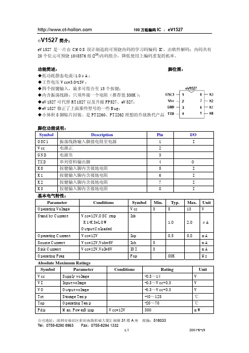
e V1527简介:eV1527是一片由CMOS设计制造的可预烧内码的学习码编码IC,由软件解码;内码共有20个位元可预烧1048576组(220)内码组合,降低使用上编码重复的机率。
功能简述:脚位图:◆低功耗静态电流<1.0μA;◆工作电压Vcc=3.0-13V;◆四个按键输入,最多可组合至15个按健;◆内含振荡线路,只须外接一个电阻(推荐值330K);◆eV1527可代替RT1527以及升级FP527、eV527;◆eV1527修正了上面那些型号的一些Bug;◆小体积8脚贴片封装。
是PT2260、PT2262理想的升级换代产品脚位功能说明:Symbol Description PinI/OOSC1 振荡线路输入脚接电阻至电源 1IVcc 电源正 2GND 电源负 3TXD 串列资料输出脚 4O K0 按健输入脚内含接地电阻 5IK1 按健输入脚内含接地电阻 6IK2 按健输入脚内含接地电阻 7IK3 按健输入脚内含接地电阻 8I基本电气特性:Parameter ConditionsSymbolMin.Typ.Max.UnitOperating V oltage Vcc 3 5 13 VStand by Current Vcc=12V,OSC stopK1-K3=LOWOutput Unloaded Isb1.02.0 μAOperating Current Vcc=12V Iop 0.5 0.8 mASource Current Vcc=12V,V oh=6V Ioh 5 mASink Current Vcc=12V,V oI=6V IOI 3 mAOperatingFreg Fop 80K Hz Absolute Maximum RatingsSymbol Parameter Conditions Rating Unit Vcc Supplyvoltage -0.3~14 V VI Inputvoltage -0.3~Vcc+0.3 VVO Outputvoltage -0.3~Vcc+0.3 VTst StorageTemp -40~125 ℃Top OperatingTemp -20~70 ℃Pdis Max.PowerDissp Vcc=12V 300 mW串列资料输出格式描述:资料格式:同步内码C0~C19(一百万组)D0 D1 D2 D3K0~K3按键组合表:K3 K2 K1 K0 D3 D2 D1 D00 0 0 1 0 0 0 10 0 1 0 0 0 1 00 0 1 1 0 0 1 10 1 0 0 0 1 0 00 1 0 1 0 1 0 10 1 1 0 0 1 1 00 1 1 1 0 1 1 11 0 0 0 1 0 0 01 0 0 1 1 0 0 11 0 1 0 1 0 1 01 0 1 1 1 0 1 11 1 0 0 1 1 0 01 1 0 1 1 1 0 11 1 1 0 1 1 1 01 1 1 1 1 1 1 1振荡阻值表:(此表仅供参考)3V 4V 5V 6V 7V 8V 9V 10V 11V 12V 13V 47K 346us 306 us 284 us 270 us 262 us 254 us 248 us 242 us 238 us 234 us 230 us51K 368us 322 us 300 us 288 us 278 us 270 us 264 us 258 us 254 us 250 us 246 us56K 400us 354 us 330 us 316 us 306 us 298 us 292 us 286 us 282 us 278 us 274 us62K 430us 384 us 358 us 344 us 334 us 326 us 318 us 312 us 308 us 302 us 300 us68K 456us 408 us 382 us 368 us 356 us 348 us 342 us 336 us 330 us 326 us 322 us75K 492us 442 us 418 us 402 us 390 us 382 us 374 us 368 us 362 us 358 us 352 us82K 528us 476 us 452 us 436 us 424 us 416 us 408 us 400 us 392 us 388 us 384 us91K 580us 524 us 492 us 480 us 468 us 456 us 448 us 444 us 436 us 432 us 424 us100K 612us 560 us 528 us 512 us 500 us 488 us 480 us 472 us 464 us 460 us 456 us120K 728us 668 us 636 us 616 us 604 us 592 us 584 us 576 us 568 us 560 us 556 us150K 872us 808 us 772 us 752 us 740 us 728 us 716 us 704 us 696 us 688 us 684 us180K 1.00ms 932 us 896 us 876 us 860 us 848 us 836 us 824 us 816 us 808 us 800 us200K 1.10ms 1.04 ms 1.00 ms 980 us 960 us 950 us 940 us 920 us 910 us 910 us 900 us220K 1.18ms 1.10 ms 1.07 ms 1.04 ms 1.03 ms 1.01 ms 1.00 ms990 us 980 us 970 us 960 us240K 1.29ms 1.21 ms 1.18 ms 1.15 ms 1.14 ms 1.12 ms 1.11 ms 1.09 ms 1.08 ms 1.07 ms 1.06 ms270K 1.44ms 1.35 ms 1.31 ms 1.29 ms 1.27 ms 1.25 ms 1.24 ms 1.22 ms 1.21 ms 1.20 ms 1.19 ms300K 1.57ms 1.47 ms 1.43 ms 1.41 ms 1.39 ms 1.37 ms 1.35 ms 1.34 ms 1.33 ms 1.31 ms 1.31 ms330K 1.69ms 1.60 ms 1.56 ms 1.53 ms 1.51 ms 1.49 ms 1.48 ms 1.46 ms 1.45 ms 1.44 ms 1.42 ms360K 1.88ms 1.78 ms 1.74 ms 1.71 ms 1.69 ms 1.67 ms 1.65 ms 1.64 ms 1.62 ms 1.61 ms 1.59 ms390K 1.98ms 1.88 ms 1.83 ms 1.81 ms 1.79 ms 1.77 ms 1.75 ms 1.73 ms 1.72 ms 1.70 ms 1.69 ms430K 2.29ms 2.17 ms 2.13 ms 2.10 ms 2.08 ms 2.06 ms 2.04 ms 2.02 ms 2.01 ms 1.99 ms 1.97 ms470K 2.38ms 2.26 ms 2.23 ms 2.20 ms 2.18 ms 2.16 ms 2.13 ms 2.12 ms 2.10 ms 2.08 ms 2.06 ms510K 2.52ms 2.40 ms 2.38 ms 2.34 ms 2.32 ms 2.30 ms 2.28 ms 2.26 ms 2.24 ms 2.22 ms 2.20 ms560K 2.76ms 2.62 ms 2.58 ms 2.56 ms 2.54 ms 2.52 ms 2.50 ms 2.48 ms 2.46 ms 2.44 ms 2.42 ms620K 3.04ms 2.92 ms 2.88 ms 2.84 ms 2.82 ms 2.08 ms 2.78 ms 2.76 ms 2.74 ms 2.70 ms 2.68 ms680K 3.32ms 3.18 ms 3.16 ms 3.12 ms 3.10 ms 3.08 ms 3.08 ms 3.06 ms 3.04 ms 3.02 ms 3.00 ms750K 3.80ms 3.68 ms 3.64 ms 3.6 ms 3.60 ms 3.56 ms 3.52 ms 3.52 ms 3.48 ms 3.44 ms 3.44 ms820K 3.92ms 3.80 ms 3.76 ms 3.76 ms 3.72 ms 3.68 ms 3.68 ms 3.64 ms 3.60 ms 3.60 ms 3.56 ms910K 4.24ms 4.14 ms 4.10 ms 4.08 ms 4.04 ms 4.02 ms 4.00 ms 3.96 ms 3.94 ms 3.90 ms 3.88 ms振荡电阻值与TD 输出关系示意图:(此图仅供参考)振荡电阻阻值TDms820K680K560K 470K360K270K 180K。
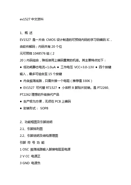
ev1527中文资料1、概述EV1527 是一片由CMOS设计制造的可预烧内码的学习码编码IC,由软件解码;内码共有20个位元可预烧1048576组(220)内码组合,降低使用上编码重复的机率。
其主要特点如下:●低功耗静态电流<1.0uA ● 工作电压VCC=3.0-13V ● 四个按键输入,最多可组合至15个按键●内含振荡线路,只需外接一个电阻(推荐值330K)●EV1527 可代替RT1527 ● 小体积8脚贴片封装。
是PT2260、PT2262理想的升级换代产品●生产极为方便,无须在PCB上编码●封装形式:SOP82、功能框图及引脚说明2.1、引脚排列图2.2、引脚说明及结构原理图引脚符号功能1 OSC 振荡线路输入脚接电阻至电源2 V CC 电源正3 GND 电源负4 TXD 串行数据输出脚5 K0 按键输入脚内置下拉电阻6 K1 按键输入脚内置下拉电阻7 K2 按键输入脚内置下拉电阻8 K3 按键输入脚内置下拉电阻2.3、功能说明输出编码的格式:同步C0-C19(100 万组) D0 D1 D2 D3 4LCK 12LCK12LCK12LCK4LCK4LCK定义:1LCK=8个OSC CLOCK同步:DATA(H):DATA(L):K0-K3 按键组合表:K3 K2 K1 K0 D3 D2 D1 D00 0 0 1 0 0 0 10 0 1 0 0 0 1 00 0 1 1 0 0 1 10 1 0 0 0 1 0 00 1 0 1 0 1 0 10 1 1 0 0 1 1 00 1 1 1 0 1 1 11 0 0 0 1 0 0 01 0 0 1 1 0 0 11 0 1 0 1 0 1 01 0 1 1 1 0 1 11 1 0 0 1 1 0 01 1 0 1 1 1 0 11 1 1 0 1 1 1 01 1 1 1 1 1 1 1振荡阻值表:(16LCK)3V 4V 5V 6V 7V 8V 9V 10V 11V 12V 13V47K 346us 306us 284us 270us 262us 254us 248us 242us 238us 234us 230us 51K 368us 322us 300us 288us 278us 270us 264us 258us 254us 250us 246us 56K 400us 354us 330us 316us 306us 298us 292us 286us 282us 278us 274us 62K 430us 384us 358us 344us 334us 326us 318us 312us 308us 302us 300us 68K 456us 408us 382us 368us 356us 348us 342us 336us 330us 326us 322us 75K 492us 442us 418us 402us 390us 382us 374us 368us 362us 358us 352us 82K 528us 476us 452us 436us 424us 416us408us 400us 392us 388us 384us 91K 580us 524us 492us 480us 468us 456us 448us 444us 436us 432us 424us 100K 612us 560us 528us 512us 500us 488us 480us 472us 464us 460us 456us 120K 728us 668us 636us 616us 604us 592us 584us 576us 568us 560us 556us 150K 872us 808us 772us 752us 740us 728us 716us 704us 696us 688us 684us 180K 1.00ms 932us 896us 876us 860us 848us 836us 824us 816us 808us 800us 200K 1.10ms 1.04ms 1.00ms 980us 960us 950us 940us 920us 910us 910us 900us 220K 1.18ms 1.10ms 1.07ms 1.04ms 1.03ms 1.01ms 1.00ms 990us 980us 970us 960us 240K 1.29ms 1.21ms 1.18ms 1.15ms 1.14ms 1.12ms 1.11ms 1.09ms 1.08ms 1.07ms 1.06ms 270K 1.44ms 1.35ms 1.31ms 1.29ms 1.27ms 1.25ms 1.24ms 1.22ms 1.21ms 1.20ms 1.19ms 300K 1.57ms 1.47ms 1.43ms 1.41ms 1.39ms 1.37ms 1.35ms 1.34ms 1.33ms 1.31ms 1.31ms 330K 1.69ms 1.60ms 1.56ms 1.53ms 1.51ms 1.49ms 1.48ms 1.46ms 1.45ms 1.44ms 1.42ms 360K 1.88ms 1.78ms 1.74ms 1.71ms 1.69ms 1.67ms 1.65ms 1.64ms 1.62ms 1.61ms 1.59ms 390K 1.98ms 1.88ms 1.83ms 1.81ms 1.79ms1.77ms 1.75ms 1.73ms 1.72ms 1.70ms 1.69ms 430K2.29ms2.17ms 2.13ms 2.10ms 2.08ms 2.06ms 2.04ms 2.02ms 2.01ms1.99ms 1.97ms 470K2.38ms 2.26ms 2.23ms 2.20ms 2.18ms2.16ms 2.13ms 2.12ms 2.10ms 2.08ms 2.06ms 510K 2.52ms2.40ms 2.38ms 2.34ms 2.32ms 2.30ms 2.28ms 2.26ms 2.24ms 2.22ms 2.20ms 560K 2.76ms 2.62ms 2.58ms 2.56ms 2.54ms 2.52ms 2.50ms 2.48ms 2.46ms 2.44ms 2.42ms 620K3.04ms 2.92ms 2.88ms 2.84ms 2.82ms 2.80ms 2.78ms 2.76ms 2.74ms2.70ms 2.68ms 680K3.32ms 3.18ms 3.16ms 3.12ms 3.10ms3.08ms 3.08ms 3.06ms 3.04ms 3.02ms 3.00ms 750K 3.80ms 3.68ms 3.64ms 3.60ms 3.60ms 3.56ms 3.52ms 3.52ms 3.48ms 3.44ms 3.44ms 820K 3.96ms 3.80ms 3.76ms 3.76ms 3.72ms3.68ms 3.68ms 3.64ms 3.60ms 3.60ms 3.56ms 910K4.24ms4.14ms 4.10ms 4.08ms 4.04ms 4.02ms 4.00ms 3.96ms 3.94ms 3.90ms 3.88m。
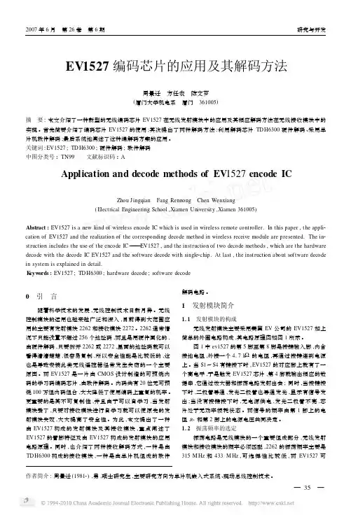
EV1527编码芯片的应用及其解码方法周景迁 方任农 陈文芗(厦门大学机电系 厦门 361005)摘 要:本文介绍了一种新型的无线编码芯片EV1527在无线发射模块中的应用及其相应解码方法在无线接收模块中的实现。
首先简要介绍了编码芯片EV1527的使用;其次提出了两种解码方法:利用解码芯片TD H6300硬件解码、采用单片机软件解码;最后系统地阐述了这种编解码方案的应用。
关键词:EV1527;TD H6300;硬件解码;软件解码中图分类号:TN99 文献标识码:AApplication and decode methods of EV1527encode ICZhou Jingqian Fang Rennong Chen Wenxiang(Electrical Engineering School,Xiamen University,Xiamen361005)Abstract:EV1527is a new kind of wireless encode IC which is used in wireless remote controller.In this paper,the appli2 cation of EV1527and the realization of the corresponding decode method in wireless receive module are presented.The in2 struction includes the use of the encode IC———EV1527,and the instruction of two decode methods,which are the hardware decode with the decode IC EV1527and the software decode with single2chip.At last,the instruction about software decode in system is explained in detail.K eyw ords:EV1527;TD H6300;hardware decode;software decode0 引 言随着科学技术的发展,无线控制技术日新月异。
AS1526, AS152710-Bit, Single Supply, Low-Power, 73ksps A/D Converters D a ta S h e e t1 General DescriptionThe AS1526/AS1527 are low-power, 10-bit, 73ksps ana-log-to-digital (A/D) converters specifically designed for single-supply A/D applications. Superior AC characteris-tics, very low power consumption, and robust packaging make these ultra-small devices perfect for battery-pow-ered analog-data collection devices.The integrated successive-approximation register (SAR) and a fast (1.5µs) sampling track/hold time provide an economic and highly-reliable A/D conversion solution. The AS1526/AS1527 operate from a single 2.7 to 3.6V supply. The AS1527 requires an external reference, using less power than the AS1526, however, theAS1526 features an internal 2.5V reference.As with the AS1527, the AS1526 can also be used with an external reference, which uses the input range 0V to V REF, including the positive supply range.The AS1527 consumes only 3mW (V DD = 3V) at the73ksps maximum sampling speed. Both devices feature a low-current (0.3µA) shutdown mode, which reduces power consumption at slower throughput rates.Data accesses are made via the standard, high-speed 3-wire serial interface, which is SPI-, QSPI-, and Microwire-compatible. Both devices contain an internal clock, however, both devices also support an external clock for increased flexibility.The AS1526/AS1527 are available in an 8-pin SOIC-150 package.Figure 1. Block Diagram and Pin Assignments 2 Key Features! 10-Bit Resolution with 7.5µs Conversion Time! Sampling Rate: 73ksps! Straight Binary (Unipolar) Data Format! Single-Supply Operation:+2.7 to +3.6V! Internal 2.5V Reference (AS1526)! Low Power-Consumption:-4mW (73ksps, AS1526)-3mW (73ksps, AS1527)-66µW (1ksps, AS1527)-1µW (Shutdown Mode)! Integrated Track/Hold Amplifier! Internal Clock! SPI/QSPI/Microwire 3-Wire Serial Interface! Operating Temperature Range: -40 to +85ºC! 8-pin SOIC-150 Package3 ApplicationsThe devices are ideal for remote sensors, data-acquisi-tion, data logging devices, lab instruments, or for any other space-limited A/D devices with low power con-sumption and single-supply requirements.AS1526/AS1527Control LogicOutputShiftRegister InternalClock10-BitTrack/Hold2.5VRefAS1526/AS15274REFAS1526onlySAR 6 DOUT5 GND1V DD7CSN8 SCLK3 SHDNN2 AIN4 REF3SHDNN2AIN1V DD5GND6DOUT7CSN8SCLKData SheetContents1 General Description (1)2 Key Features (1)3 Applications (1)4 Pinout and Packaging (3)Pin Assignments (3)Pin Descriptions (3)5 Absolute Maximum Ratings (4)6 Electrical Characteristics (5)Timing Characteristics (7)7 Typical Operating Characteristics (8)8 Detailed Description (11)Analog Input (11)Input Protection (12)Track/Hold (12)External Clock (12)Timing and Control (12)Transfer Function (14)Reducing Supply Current (14)Internal 2.5V Reference (AS1526) (15)External Reference (15)9 Application Information (16)Initialization (16)Serial Interface (16)Serial Interface Configuration (16)SPI and Microwire Interfaces (16)QSPI 17Layout Considerations (18)Package Drawings and Markings (19)10 Ordering Information (20)Data Sheet - Pi n o u t a n d P ac k a gi n g4 Pinout and PackagingPin AssignmentsFigure 2. Pin Assignments (Top View)Pin DescriptionsTable 1. Pin Descriptions Pin NumberPin Name Description1V DD Positive Supply Voltage . +2.7 to +3.6V 2AINSampling Analog Input . 0V to V REF range.3SHDNNThree-Level Shutdown Input . Pulling this pin low puts the AS1526/AS1527 in shutdown mode, down to 4µA (max) supply current. The devices are fully operational with this pin high or floating.Note:For the AS1526, pulling this pin high enables the internal reference; let-ting this pin float disables the internal reference allowing for the use of an external reference. See also pin 4.4REFA/D Conversion Reference Voltage . This pin serves as the internal 2.5V reference output for the AS1526; bypass this pin with a 4.7µF capacitor.This pin also serves as the external reference voltage input for the AS1527, or for AS1526 if the internal reference is disabled. Bypass this pin with a minimum of 0.1µF when using an external reference. See also pin 3.5GND Analog and Digital Ground6DOUT Serial Data Output . Data changes state at SCLK’s falling edge.Note:This pin is high-impedance when pin CSN is high.7CSN Active-Low Chip Select . The falling edge of this pin initiates a conversion.Note:When this pin is high, DOUT is high-impedance.8SCLKSerial Clock Input . This pin clocks data out at rates up to 2.1MHz.AS1526/AS15274REF 3SHDNN 2AIN 1V DD 5GND6DOUT7CSN8SCLKData Sheet- Ab s o l u te M a x i m u m R a t in g s5 Absolute Maximum RatingsStresses beyond those listed in Table 2 may cause permanent damage to the device. These are stress ratings only, and functional operation of the device at these or any other conditions beyond those indicated in Section 6 Electrical Characteristics on page 5 is not implied. Exposure to absolute maximum rating conditions for extended periods may affect device reliability.Table 2. Absolute Maximum RatingsParameter Min Max Units CommentsV DD to GND0.3+5VAIN to GND-0.3V DD +0.3V VREF to GND-0.3V DD +0.3V VDigital Inputs to GND-0.3V DD +0.3V VDOUT to GND-0.3V DD +0.3V VDOUT Current-25+25mAContinuous Power Dissipation(T AMB = +70ºC)471mW Derate 5.88mW/ºC above +70ºC Operating Temperature Range -40+85ºCStorage Temperature Range-60+150ºCPackage-Body Peak Temperature 260 °C The reflow peak soldering temperature (body temperature) specified is in accordance with IPC/JEDEC J-STD-020C “Moisture/Reflow Sensitivity Classification for non-hermetic Solid State Surface Mount Devices”.6 Electrical CharacteristicsV DD = +2.7 to +3.6V, 73ksps, f SCLK = 2.1MHz (50% duty cycle); AS1526:4.7µF capacitor at REF, AS1527: external ref-erence; V REF = 2.5V applied to REF; T AMB = T MIN to T MAX (unless otherwise specified). Table 3. Electrical Characteristics Symbol Parameter Conditions Min Typ Max UnitsDC Accuracy1Resolution 10 Bits Relative Accuracy 2±0.5 LSB DNL Differential Non-Linearity No missing codes over temperature±1 LSB Offset Error ±2LSBGain Error 3±2 LSBGain Temperature Coefficient±1ppm/°CDynamic Specifications (10kHz sine-wave input, 0V to 2.5Vp-p, 73ksps, f SCLK =2.1MHz) SINADSignal-to-Noise + Distortion Ratio61dB THD Total Harmonic Distortion Up to the 5th harmonic-70 dB SFDR Spurious-Free Dynamic Range70 dB Small-Signal Bandwidth -3dB rolloff2.5 MHz Full-Power Bandwidth2.5MHzConversion Ratet CONV Conversion Time 5.5 7.5 µst ACQTrack/Hold Acquisition Time1.5µs Throughput Rate 4f SCLK = 2.1MHz 73ksps t AP Aperture DelayFigure 27 on page 137ns Aperture Jitter<50 psAnalog InputInput Voltage Range 0V REF VInput Capacitance21pFInternal Reference (AS1526 only)REF Output Voltage T AMB = +25ºC52.47 2.50 2.53V REF Short-Circuit Current 45mA REF Temperature CoefficientAS1526±30 ppm/°C Load Regulation 60 to 0.2mA output load0.35mVC REFBYPCapacitive Bypass at REF 4.7 µFExternal Reference (V REF = 2.5V)Input Voltage Range1.00 V DD +50mV V Input Current 100150µA Input Resistance1825 k ΩREF Input Current in ShutdownSHDNN = 0V±0.0110 µAC REFBYPCapacitive Bypass at REF 0.1 µFDigital Inputs : SCLK, SHDNN, CSN V IH SCLK, CSN Input High Voltage 0.7x V DDV V IL SCLK, CSN Input Low Voltage 0.3x V DDV V HYST SCLK, CSN Input Hysteresis 0.2 VI IN SCLK, CSN Input Leakage V IN = 0V or V DD ±0.01±1 µAC IN SCLK, CSN Input Capacitance 715pF V SH SHDNN Input High Voltage V DD -0.4V V SLSHDNN Input Low Voltage 0.4 VSHDNN Input CurrentSHDNN = 0V or V DD ±4.0µA V SM SHDNN Input Mid Voltage 1.1V DD - 1.1VV FLTSHDNN Voltage, Floating SHDNN = float V DD /2 VSHDNN Max Allowed Leakage,Mid InputSHDNN = float±50nADigital Output : DOUT V OL Output Voltage Low I SINK = 5mA 0.4 V I SINK = 16mA 0.8V OH Output Voltage High I SOURCE = 0.5mAV DD - 0.5VI L Tri-State Leakage Current CSN = V DD ±0.01 ±10µA C OUTTri-State Output CapacitanceCSN = V DD715pFPower RequirementsV DD SupplyVoltage 2.7 3.6 V I DD SupplyCurrent Int. Reference (AS1526), V DD = 3.6V1.42.0 mA External Reference, V DD =3.6V 1.0 1.4 Shutdown mode, V DD = 3.6V0.32µAPSRPower-Supply Rejection8V DD = V DDMIN to V DDMAX ,full-scale input±1 mV1.Tested at V DD = +2.7V.2.Relative accuracy is the deviation of the analog value at any code from its theoretical value after the full-scale range and offset have been calibrated.3.Offset nulled.4.Achievable with standard timing (see Figure 25 on page 13).5.Sample tested at 0.1% AQL.6.External load should not change during conversion for specified accuracy.7.Guaranteed by design; not subject to production testing.8.Measured as [V FS (V DDMIN ) - V FS (V DDMAX )] with external reference.Table 3. Electrical Characteristics (Continued)SymbolParameterConditionsMin TypMaxUnitsTiming CharacteristicsV DD = +2.7 to +3.6V, T AMB = T MIN to T MAX (unless otherwise specified).Figure 3. DOUT Enable-Time Load CircuitsFigure 4. DOUT Disable-Time Load CircuitsTable 4. Timing CharacteristicsParameter Symbol Conditions Min Typ Max UnitsAcquisition Time 11.To guarantee acquisition time, t ACQ is the maximum time the device takes to acquire the signal, and is also theminimum time needed for the signal to be acquiredt ACQ 1.5 µsSCLK Falling-to-DOUT Valid t DO Figure 3, C LOAD = 50pF 20200 ns CSN Falling-to-Output Enable t DV Figure 3, C LOAD = 50pF 240ns CSN Rising-to-Output Disable t TR Figure 4, C LOAD = 50pF240nsSCLK Clock Frequency f SCLK 0 2.1MHzSCLK Pulse Width High t CH 200ns SCLK Pulse Width Low t CL200 nsSCLK Low-to-CSN Falling SetupTime t CS0 50 ns DOUT Rising-to-SCLK Rising 22.Guaranteed by design; not subject to production testing.t STR 0 nsCSN Pulse Widtht CS240 nsC LOAD 50pFC LOAD 50pF 6k ΩGNDDGNDDOUTDOUTHigh-impedance to V OH and V OL to V OH+2.7VHigh-impedance to V OL and V OH to V OL6k ΩDGND6k ΩC LOAD 50pFC LOAD 50pF 6k ΩDGNDGNDDGNDDOUTDOUTV OH to high-impedance+2.7VV OL to high-impedance7 Typical Operating CharacteristicsV DD = 3.0V, V REF = 2.5V, f SCLK = 2.1MHz, C LOAD = 50pF, T AMB = +25ºC (unless otherwise specified).分销商库存信息:AMSAS1527-BSOU AS1526-BSOU AS1527-BSOT AS1526-BSOT。