2 EMI filter design Part II Measurement of noise source impedances
- 格式:pdf
- 大小:1.16 MB
- 文档页数:8

压缩气过滤器设计与选型标准英文回答:Design and Selection Criteria for Compressed Air Filters.Compressed air filters are essential components in many industrial applications as they help remove contaminants and impurities from the compressed air system. The design and selection of these filters are crucial to ensure the efficient and reliable operation of the system.When designing and selecting compressed air filters, there are several important criteria to consider:1. Filtration Efficiency: The primary function of a compressed air filter is to remove contaminants from the air. The filtration efficiency of a filter is typically measured in microns, indicating the size of particles it can effectively capture. A higher filtration efficiencymeans that the filter can remove smaller particles, resulting in cleaner compressed air.2. Pressure Drop: The pressure drop across the filteris another important consideration. As air passes through the filter, it encounters resistance, which leads to a pressure drop. A high-pressure drop can affect the overall system performance and increase energy consumption. Therefore, it is crucial to select filters with low pressure drop to minimize the impact on the system.3. Flow Rate: The flow rate of compressed air is another critical factor to consider. The filter should be capable of handling the maximum flow rate required by the system without causing any restrictions or pressure drops. It is essential to choose filters that can accommodate the specific flow rate requirements of the application.4. Filter Media: The filter media plays a vital role in the filtration process. It is important to select a filter with the appropriate media that can effectively capture and retain contaminants. Common filter media include cellulose,polyester, and activated carbon. The choice of filter media depends on the type of contaminants present in the compressed air and the desired level of filtration.5. Maintenance and Serviceability: Filters require regular maintenance and replacement to ensure optimal performance. It is important to consider the ease of maintenance and availability of replacement parts when selecting a filter. Filters with easy access to the filter element and quick-change features can significantly reduce downtime during maintenance.In conclusion, when designing and selecting compressed air filters, it is essential to consider factors such as filtration efficiency, pressure drop, flow rate, filter media, and maintenance requirements. By carefully evaluating these criteria, one can choose the most suitable filter for their specific application, ensuring clean and reliable compressed air supply.中文回答:压缩气过滤器设计与选型标准。
进行mechanical分析的步骤:1)建立几何模型:在Pro/ENGINEER中创建几何模型。
2)识别模型类型:将几何模型由Pro/ENGINEER导入Pro/MECHANICA中,此步需要用户确定模型的类型,默认的模型类型是实体模型。
我们为了减小模型规模、提高计算速度,一般用面的形式建模。
3)定义模型的材料物性。
包括材料、质量密度、弹性模量、泊松比等4)定义模型的约束。
5)定义模型的载荷。
6)有限元网格的划分:由Pro/MECHANICA中的Auto GEM(自动网格划分器)工具完成有限元网格的自动划分。
7)定义分析任务,运行分析。
8)根据设计变量计算需要的项目。
9)图形显示计算结果。
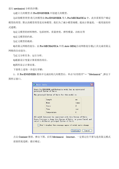
下面将上述每一步进行详解:1、在Pro/ENGINEER模块中完成结构几何模型后,单击“应用程序”→“Mechanical”,弹出下图所示窗口,点击Continue继续。
弹出下图,启用Mechanical Structure。
一定要记住不要勾选有限元模式前面的复选框,最后确定。
2、添加材料属性单击“材料”,进入下图对话框,选取“More”进入材料库,选取材料Name---------为材料的名称;References-----参照Parrt(Component)-----零件/组件/元件V olumes-------------------体积/容积/容量;Properties-------属性Material-----材料;点选后面的More就可以选择材料的类型Material Orientation------材料方向,金属材料或许不具有方向性,但是某些复合材料是纤维就具有方向性,可以根据需要进行设置方向及其转角。
点选OK,材料分配结束。
3、定义约束1):位移约束点击,出现下图所示对话框,Name 约束名称Number of Set 约束集名称,点击New可以新建约束集的名称。
Reference 施加约束时的参照,可以是surfaces(面)、edges/curves(边或曲面)、points(点)等Coordinate System 选择坐标系,默认为全局坐标系Translation 平动约束(Free为自由,fixed为固定,Prescribed为指定范围)Rotation 旋转约束单位为度Individual--------------单独的、孤立的Surf Options----------面选项Part Boundary---------零件的选择。
AEC - Q003July 31, 2001Component Technical CommitteeAutomotive Electronics CouncilAEC – Q003July 31, 2001 Automotive Electronics CouncilComponent Technical CommitteeAcknowledgmentAny document involving a complex technology brings together material and skills from many sources. The Automotive Electronics Council would especially like to recognize the following significant contributors to the development of this document:Majdi Mortazavi DaimlerChrysler (256)464-2249 msm11@Brian Jendro DaimlerChrysler (256)464-2980 bj5@Detlef Griessman Delphi Delco Electronics Systems (765)451-9623 detlef.griessman@Robert V. Knoell Visteon Corporation (313)755-0162 rknoell@Nick Lycoudes Motorola (408)413-3343 raqa01@Mark Yasin Motorola AIEG (830)372-7200 Mark_Yasin-GUSR243@ Philippe Briot PSA, Peugeot, Citroën 33 01 41 36 7849 p-briot@psinet.frMark Gabrielle On Semiconductor (602)244-3115 mark.gabrielle@Enrico Valacca Magneti Marelli 39 382 59 9650 enrico.valacca@pavia.marelli.itWilhelm Mayer Temic 49 841 881 2321 wilhelm.mayer@Jeff Parker International Rectifier (909)375-4415 jparker1@Gerald E. Servais Delphi – retired (765)883-5473 gervais@Component Technical CommitteeGuidelineForThe Characterization of Integrated Circuits1. PURPOSE:The characterization of ICs is an extremely important function during the development of a new IC or the modification of an existing IC. The purpose of this document is to provide guidance by highlighting important considerations that should be evaluated during development of acharacterization procedure. This document is not intended to be a specification on how toperform a characterization. To ensure consistent characterization every company should have a structured and documented characterization procedure. The characterization process should be used to ensure that the design & wafer fab/assembly processes being utilized demonstratesufficient capability of providing a part that meets the requirements of the customer. The results of every characterization should be documented in a Characterization Report.2. SCOPE:This guideline document provides the basis for establishing a procedure for characterizing the electrical performance of Integrated Circuit products. This characterization procedure should be used for new technologies, new wafer fabrication processes, new product designs andsignificantly modified ICs.3. DEFINITIONS:3.1 Device Electrical ParametersElectrical measurements specified in the part specification for the device, and / or othermeasurements as indicated by engineering experience for the technology involved.3.2 CharacterizationThe process of determining the fundamental electrical and physical characteristics (voltage,frequency, and temperature behavior) of a device based on statistical analysis of experimental data or modeling. This includes the distribution of an electrical parameter as a function of other parameter(s) variation. The graphical presentation of the characterization for a typical electrical parameter is a multivariate hyper - ellipsoid, see Figure 1 (frequently called a Schmoo Plot).Component Technical Committee Figure 1 Schmoo Plot3.3 Criteria For CharacterizationA device that meets the following criteria should be considered a candidate for characterization.This criteria should not be considered a limitation but a starting point for factors to consider.• new chip layout or changes to an existing die that could impact electrical parameters (e.g., die shrink)• new cell structure(s) which have not been used in production components• new processing methods or materials• new operating bias condition requirements (re-characterize at new bias extremes)• significant increase in operating environmental condition requirements (re-characterize at new environmental extremes)3.4Specification Limits (e.g., data sheet limits):Numerical values of maximum, minimum, and typical electrical parameters specified in the customers part specification or the supplier data sheet. These values are used to determine pass / fail criteria for the characterization.3.5 Guard Bands:The difference between test limits and specification limits. Test limits are generally tighter than specification limits to account for tester inaccuracies and other sources of variation.4. CHARACTERIZATION PROCEDURE:This guideline is not intended to establish the characterization process / procedure, but is intended to provide an outline of factors that should be considered when establishing acharacterization procedure. Every supplier should establish a characterization procedure. The characterization procedure should include the following major activities for the device to be characterized:Test Limit Each dot is a measurementfrom one partGuard Band measurementSpecification limit Parameter 1Pa ra m et er 2Par a me t e rComponent Technical Committee•Review of PFMEA (process FMEA), DFMEA (design FMEA) and the related Control Plans or equivalent methods that link failures to the manufacturing process and designprocess.•Determination of the characterization method to be used.•Establishment of the parameters to be characterized.•Completion of a characterization report.4.1 Device Characterization:The characterization of new parts requires a procedure that provides in-depth information about the capability of the part design / process to produce the part. Before beginning thecharacterization procedure review the Characterization Checklist, see Appendix 1. Thischaracterization procedure should include measuring to the part specification requirementsacross the operating voltages, frequencies, and temperatures or the use of documentedsimulation methods. (Note: Although not included in the characterization, it is important todetermine the ESD, Latch-up, and Generic Leakage capability of a part early in the development cycle as these parameters could have a significant impact on the performance of the part.) The characterization methods used (see Appendix 2, and 3) should be clearly documented in aCharacterization Report.4.2Characterization ReportThe characterization report should include the following:1. A summary of the PFMEA (Process FMEA) and DFMEA (Design FMEA) and the relatedControl Plans or equivalent methods that link failures to the manufacturing process anddesign process.2. A detailed discussion of the characterization methods used (see Appendixes 1, 2, and3).3. A listing of all critical parameters monitored during the characterization. A listing of allcritical parameters that do not show a Design Index of 1 or greater (see Appendix 4) or aCpk of 1.33 to the specification test limits.4.Discussion of device weaknesses and corrective actions, both design and processrelated.5.Containment plans for handling uncorrected part weaknesses and reliabilityconcerns. (e.g., voltage stress test or burn-in to contain gate oxide defects.)6.The report should be approved by a responsible supplier representative.The results of the characterization should be shared with the customer (at the discretionof the supplier this sharing may include a hard copy of the characterization report or selectedportions of the characterization report).Component Technical CommitteeAPPENDIX 1Characterization ChecklistThe following points should be evaluated during the planning stage for product characterization:•Have all the cell structures used in this product been characterized?•Has the wafer fab process changed since the cell structure characterizations?•If the wafer fab process has changed, do the simulation models that will be used for characterization account for all wafer fab process changes?•If matrix devices will be needed, which process windows should be involved in the matrix? What is the worst case variation in these process windows? (Note: The worst case processing variation should be based on the worst case conditions observed during the last six months or expected during normal manufacturing.) Who should participate in making these decisions?•Are there matrix cell interactions that should be considered?•How can simulation models be used to simplify and expedite the characterization process? How good are the available simulation models? What is the confidence in the simulation models? What are the risks if the available simulation models are used?•Have the drift characteristics of the cell structures been characterized? Is a device parameter drift analysis needed as part of this characterization?•Are there stresses associated with the product package that could affect the initial and late life electrical parameters of the product?•If matrix units are required, how many (sample size) from each matrix cell? How many process variations need to be characterized? Will the product be characterized beyond the required part specification requirements (hotter or colder temperatures, higher or lower frequencies, higher or lower bias voltages)? Will the software required for the characterization be available when needed?•Do we know the junction temperatures (hot and cold) that must be evaluated in this characterization?Have the thermal characteristics of the measurement system(s) been considered, see Appendix 3?•What form will matrix devices be in for the characterization – packaged? .. wafer level? Have packaging requirements been included in the characterization plan?•Will the ESD, Latch-up, and Generic Leakage capability be evaluated early in the development cycle?•Are DFMEAs and PFMEAs available for other products manufactured with the same Process Control Limits? Is a new DFMEA and PFMEA required for this product? Who should be involved in the team preparing the DFMEA and PFMEA for this product?Component Technical CommitteeAPPENDIX 2Test Die SelectionOne goal of characterization is to discover potential problems during early development when changes can be made quickly, easily, and less expensively. Therefore, caution should be exercised so that pre-testing before characterization is minimized, since it has the possibility of truncating the normal matrix cell distribution and hiding potential problems.The recommended pre-testing approach is to only eliminate non-functional devices from the characterization sample.Examples to help define non-functional - the following would be considered test limits for functional devices:1) Override specification required parametric failures and only perform relaxed spec functional tests(EZ-functional).2) Widen all specification required parametric limits by a significant digit.The method of selecting die can have a large effect on the amount of inherent process variation that is included in the data. The main concern is to understand and design for the largest sources of inherent process variation. Due to the number of different process technologies it is the responsibility of the supplier to develop a combination of lots, wafers, and die locations that will provide the inherent process variation.A thorough analysis of sample size should also consider the following:1) Which wafers are selected for a cell?2) Which die locations are selected on a wafer?Component Technical CommitteeAPPENDIX 3Characterization TestingThe die selected for characterization shall be tri-temperature tested. Test temperatures need to be established for room, hot, and cold test. The test setup temperature extremes should be able to duplicate worst case product application junction temperatures.It should be stressed that the junction temperature of the device in the selected operating condition is the actual characterization target. For example, a low test temperature limit of -55ºC might be required for a -40ºC instantaneous customer need (i.e. operate on cold wake-up) to account for a 15ºC steady state heating during testing. Likewise, a high test temperature limit of 135ºC might be required for a 150ºC instantaneous package test to account for a 15ºC steady state heating during testing.The bias conditions and subsequent power consumption will determine if there is sufficient energy dissipation to necessitate the need for test temperature correction(s). In some situations an instantaneous condition is assumed that would null the effects of thermal dissipation, while in other conditions a high energy steady-state condition is assumed that would necessitate the use of temperature correction(s).Example:Simulate a Customer Junction Temperature of 155ºC -If the starting temperature of a customer system is ………125ºCAnd a thermal gradient (w/bias condition) causes atemperature increase of ……………………………… 30ºCThen the customer junction temperature requirementis …….……………………………….……………….. 155ºCCharacterization Test Temperature -The junction temperature to simulate is ………….……….. 155ºCIf the steady state heating during testing causes athermal gradient (w/bias condition) thatresults in a temperature increase of …….….….…. 15ºCThen, the required final test setup temperature(Characterization test temperature) is ….…….….. 140ºC **Note: Additional temperature may be added to this value for guardbanding.Component Technical CommitteeAPPENDIX 4Design IndexThe idea of representing the goodness or badness of a product's Device Parameter performance (over the worst case expected variation in Key Fab Process limits) with a single value is the reason for establishing a Design Index (DI). A Design Index of 1 or greater for a particular parameter requirement means that the device meets that parameter requirement at all matrix points. ( Note: A Design Index of less than 1 indicates that a particular parameter will probably cause a higher yield loss during normal production.)This section will discuss the theory behind the DI and how to use it.In a matrix characterization (or simulation), processing variables are forced to certain values (to form matrix cells) and the product performance is evaluated. The goal of the characterization is to determine if the device performance will stay within specification limits when processing variables are forced to their worst case values, see Appendix 1.The Device Parameters are the values measured (or modeled), or tests performed, to ensure that the device meets all of the electrical requirements defined in the Part Specification. In general, the Device Parameters measured on parts taken from different cells of the matrix will have different values. Each part parameter, then, will have a performance range, the result of parts being tested from different cells of the matrix, see Figure 4 - 1.(at one test temperature)Figure 4 - 1 Typical Matrix Parameter RangeComponent Technical Committee In defining the DI it is assumed that the Device Parameter population that is sampled in each matrix cell is normally distributed and independently distributed. The index also assumes that the product would yield equally well when processed at any point within the Design / Process window. Thus, there is no weighting of the matrix data.The actual definition of DI is very similar to that of the Cpk index. The important difference is that the Cpk is based on a single normal distribution (grouping all matrix cells into one distribution) while the DI is based on the worst case of several individual matrix distributions, see Figure 4 - 2.Figure 4 - 2 Comparison of Cpk and Design IndexThe DI (one number for each Device Parameter upper and lower specification limit) is determined as follows:1. Statistically analyze the electrical distribution characteristics for each matrix cell, device parameter, and test temperature. (The statistical analysis should include an estimation of the mean and the worst case edges for each distribution, and should be based on the confidence interval (ci) on the estimated mean, see Figures 4 – 3.) For example, if there are 5 matrix cells (as shown in Figure 4 -1) and three test temperatures, there will be 15 distributions (5 at each temperature) for each Device Parameter, see Figure 4 - 4.2. Using the Extreme W L (A) and Extreme W U (B), as shown in Figure 4-3, calculate the mean [M =(A + B) / 2].3. Then, determine the DI values (DI lower and DI upper) for each parameter) as shown in Figure 4-4.LowerUpper (Assuming Upper Spec is the closer Spec)For a single Normal distribution ...C pk = (Upper Spec - xbar) / 3s= (USPL - xbar) / 3sOver the entire Matrix ...Design Index = (Upper Spec - M)/ (W U - M)M = (A+B) / 2A = worst W LB = worst W USee Figure 4-3 for definition of W L , W UComponent Technical CommitteeFigure 4 - 3 Statistical Analysis Including The Confidence IntervalTrue DeviceParameter Population (unknown)= confidence interval (ci) on sample meanL = xbar - ci - 3s U = xbar + ci +3sComponent Technical CommitteeFigure 4- 4 Analysis of Five Matrix Cells at Three Temperatures.AM = (A+B) / 2BB = Extreme W UA = Extreme W LLower Spec (LSPL)Upper Spec (USPL)DI lower = "Di L " = (M - LSPL) / (M - A)DI upper = "Di U " = (USPL - M) / (B - M)Component Technical CommitteeRevision HistoryRev #Date of change Brief summary listing affected sections -- July 31, 2001 Initial release。

实验三IIR滤波器的设计1. Specification: The first step in designing an IIR filter is to specify the desired frequency response characteristics. This includes the cutoff frequency and the desired stopband attenuation. These specifications will determine the type of filter and its order.2. Filter type selection: Based on the specifications, we need to choose the appropriate filter type. There are various types of IIR filters, such as Butterworth, Chebyshev, andElliptic filters, each with different characteristics.4. Transfer function design: Once the filter order is determined, we can design the transfer function of the filter. This involves finding the coefficients of the numerator and denominator polynomials that represent the filter's transfer function.5. Filter implementation: Depending on the application, the designed filter can be implemented using different methods such as analog electronic circuits, digital signal processing algorithms, or field-programmable gate arrays (FPGAs).6. Filter validation: After implementing the filter, it needs to be validated to ensure it meets the specified requirements. This can be done by applying test signals to the filter and analyzing the output. Various performance metrics canbe used for validation, such as magnitude response, phase response, and group delay.7. Filter optimization: If the filter does not meet the desired specifications, optimization techniques can be used to adjust the filter parameters and improve its performance. Optimization algorithms can be used to minimize the error between the desired and actual frequency response.However, IIR filters have some limitations. They may introduce phase distortions, especially in the stopband region, which can be problematic for certain applications. IIR filters are also sensitive to quantization errors in digital implementations, requiring careful consideration of word-length and fixed-point arithmetic.In conclusion, the design of IIR filters involves several steps, from specifying the desired frequency response characteristics to implementing and validating the filter. It is important to choose the appropriate filter type and order based on the application requirements. Additionally, optimization techniques can be used to improve the filter's performance if it does not meet the desired specifications.。
IntroductionWhether you are a telecommunications service provider or a telecommunications equipment manufacturer, the global market-place has requirements for a multitude of signaling protocols within countries and between countries.In-service circuits need troubleshooting. New products need testing and, eventually, manufac-turing test and field support. Until now, the only solution may have been numerous test instru-ments or expensive in-house test equipment development for each country or application.The Ameritec Model AM8e is a Call Analyzer capable of emulating, observing and trouble-shooting signaling protocols on a wide variety of analog circuits or 2 Mbps channel associated signaling PCM circuits. The AM8e is user programmable. You can modify existingsignaling protocols or develop new signalingprotocols based on your requirements. 2 Mbps PCM Testing The AM8e is compatible with worldwide CCITT recommendations for 2 Mbps, 30-channel, channel associated signaling PCM lines.The unit is compatible with all country specific A, B, C, D bit signaling and MF-R1, MF-R2,CCITT #5, DTMF, and dial pulse protocols.The AM8e provides for emulation and non-intrusive monitoring of 2 Mbps PCM circuits.Specific channels can also be monitored. Also provided is a drop and insert capability which allows testing of individual PCM plete decoding and analysis of MF-R1,MF-R2, CCITT #5, DTMF, and dial pulse signaling is provided. Precise, one-millisecond time stamping of digits and events will tell you exactly what happened and when.Exception reports can be printed by connecting an accessory printer and using the built-in programmable signaling thresholds to automati-cally screen for out of tolerance digits and events.User Programmable Signaling ProtocolsTo provide the utmost in flexibility to accommo-date worldwide signaling variations, the AM8e is protocol driven. Protocols may be purchased from Ameritec’s extensive library, custom developed by Ameritec or developed by the user. The AM8e can store up to 10 complex protocols which can be simply recalled and executed. The protocols allow for various W AIT conditions, such as Wait for 3Seconds, Wait For Call Progress Tone, Wait For Wink and so on. The protocols can select any of the available 10 autodial strings and each string can point to another string for virtually unlimited dialed digit lengths. Calling and called party numbers may be stored in different autodial strings and executed at the appropriate stimulus from within the protocol. Dialing may be dependent upon a Wait condition. These capabilities allow the user to test complex Intelligent Network functions as well as CTI applications such as V oice Mail.Protocols can also cause tones to be transmitted with a specific level and frequency. For dual tone dialing, the level and frequency of each tone of the two tones can be specified, allowing for testing of an application over the full range of specified dialed digit capability. Simple loops can be set up in a protocol for incremental worst case testing. Analog Loop Trunk/Line EmulationThe AM8e is also compatible with two-wire analog type trunks and lines. User programmable emulation, monitoring and analysis are provided for the following parameters:• Battery V oltage, Loop Length & Termination • Start Dial Signals including Dial Tone • MF-R1, DTMF & Dial Pulse Signaling • Dial Pulse Speed, Make/Break & Interdigit Time• MF/DTMF Digit Timing,Twist &Skew • Dial Tone Delay, Cadence,Frequencies & Level • Hookflash & Line Unbalance• Ringing V oltage, Frequency & Cadence • Delay & Wink Start Signals• Single Test Tone Frequency & Level The analysis functions allow measurement thresholds to be set in order to capture erroneous digits and events. This, along with the precise,one-millisecond time stamping of digits and events, allows detection of even the most subtle problems.AM8e with E&M Adapter.AM8e E&M Adapter The AM8e E&M Adapter replaces the protective front panel cover of the AM8e and offers conve-nient access to analog E&M signaling emulation,monitoring, and analysis capabilities. This includes North American standards too! Simply attach the E&M Adapter to the LINE/TIMS Connector of your AM8e with the ribbon cable and you are ready to apply the same troubleshooting and testing power available for PCM and two-wire loop circuits.In combination with the AM8e, the E&M Adapter provides the following analog E&M capabilities:•E&M Signaling Emulator/Monitor/Analyzer •E&M Types I through V , 2-Wire and 4-Wire •4-Wire E&M and 4-Wire Phantom E&M •Programmable Signaling Protocols to Control E&M Leads •Digit Emulator/Monitor/Analyzer (MF-R1, MF-R2, CCITT #5, DTMF, Dial Pulse)•Complex Sequence Dialer •High/Low Thresholds for Capturing Erroneous Digits and Events •Precise, One-Millisecond Time Stamping of Digits and Events •VF Level, Frequency and Noise Measure •CO Battery and Dial Tone Generator Ameritec E&M signaling protocols are available or users may develop their own protocols.T1/E1 Adapter The AM8e T1/E1 Adapter replaces the protec-tive front panel cover of the AM8e. The Adapter converts the AM8e E1 input/output to T1input/output and accommodates both PCM1 and PCM2. With this Adapter the power of the AM8e protocols can be used in a T1 environment to allow test of very complex interface protocols.Additionally, an AM8e with this Adapter can also be used for standard T1 testing, significantly improving the utility and versatility of the AM8e.Off Hook Display Selection for Events or VoltmeterDirect Entry KeypadFar End Start Dial Out of Dialing Digits (Near End)Far End Answer ON/OFF Power ButtonVolume control for speaker Microphone to communicate over circuit under test Connection of telephone handset for private conversations Connection of external Transmission Impairment Measuring Set (such as Ameritec's AM5eXT)• RS232 Port for exception reporting & remote control.• Decoding of MF-R1, MF-R2, CCITT #5, DTMF and dial pulse digits without pre-determination of type.• Built-in Speaker.• Optional Battery Pack for 8 Hours Use Visual LED indicators to show configuration of unit.Near End On Hook Analog Loop Connection2 Mbps PCM span connections Grouping of Direct Function Switches Scrolling up &down pages within each setup menu Scrolling across choices for setup parameters Unit setup including emulation parameters.Analyzer Thresholds and Auto Dial sequences ON/OFF Toggles for connection to Trunk inputs & TIMS.Enable hands-free talk and auto send of start signalDialed MF-R2 Digits each followed by a backward acknowledge digit.Time from off-hook to MF-R2 forward digit 8, level/freq. low tone, level/freq. high tone,and interdigit time/digit duration.Detailed Call AnalysisFar End On Hook Display of A/B signaling bits for all 30 E1 time slots (transmit and receive).Detailed Digit, Event Analysis When connected to a circuit, the unit will display signaling events occurring in either direc-tion on a large backlighted liquid crystal display (LCD). Up to 80 dialed digits and/or events (on hook, off hook, wink, etc.) are collected and displayed for each call.By merely placing a cursor under the digit or event of interest, the operator can observe, on the second line of the display, all details associated with that event. For example, when observing a DTMF digit, the unit will display the time of the digit and its duration, as well as the measured high and low band frequency and level.If the operator had previously entered good/bad thresholds, then any out-of-spec detail would be highlighted to the operator.With each event in a complexsequence captured in detail,troubleshooting becomes a matter of solving the problem instead ofsearching for the problem.Built-in Analog and PCM Testing The ability to measure VF level, frequency and noise on analog circuits and PCM channels is built into the AM8e. For more extensive testing, a TIMS access port is provided.The unit also provides a variety of non-intrusive PCM digital tests including bit and frame slips,CRC errors, and framing errors. A display of all 30 PCM channel A/B signaling bits can also be viewed for the transmit and receive directions.All front panel test ports appear on the rear panel LINE/TIMS connector which simplifies integration into a test system.Complex Sequence Auto-Dialer Through the front panel keypad or via a protocol, the operator can dial any sequence of digits and events either manually or automati-cally. Up to 10 complex dialing sequences can be stored and later recalled for execution under the “autodial” function. One autodial sequence can “point” to another so that a complex dialing routine can effectively be hundreds of events long.For example, the following sequence might be used to initiate test calls from a PABX station and use multiple signaling modes to reach and communicate with specialized equipment.PCM Drop & Insert The AM8e provides two PCM ports with dual receivers andtransmitters.These ports canbe usedforpassivemonitoring of a PCM span or the AM8e may be inserted in series with the PCM span for full duplex drop and insert testing of individual channels.The two PCM ports can also be used for clock synchronization testing of PCM spans where one port is connected to a reference span while the second port is connected to the span under test.Easy Setup Commonly used AM8e test setups can be stored in non-volatile memory for later use. 20 non-volatile memories are available for instant recall of personalized AM8e configura-tion setups. An additional 20 memories are availablefor recall of emulate/analyze parameters. This is in addition to the previouslymentioned memories for 10 auto-dial sequences plus last number redial.High Tech, Small SizeThe AM8e incorporates multiple digital signal processors and microprocessors in a highly compact portable package. The unit may be powered from commercial mains, where it automatically adjusts for compatibility with local line voltage and frequency, or it may be powered from an optional internal rechargeable battery pack. An optional RS232 port and aux port allows for automatic hard copy reporting and remote control. A 24-pin LINE/TIMS connector on the rear of the AM8e provides secondary access to all front panel connections and is useful for perma-nent AM8e installations in systems and other test equipment.Dual PCM ports.Easy setup store and recall.Rear of AM8e with RS232 ports for hard copy output and remote control.Simulated Voice Response System Test CallAM8e shown in rack mount configuration.Built-in VoltmeterA dual multimeter with analog and digital display is provided. AC volts, DC volts, and current measurements may be operator selected for tip to ring, tip to ground or ring to ground connections. PCM signal amplitude can be measured when using the AM8e in PCM mode.Portable or Rack Mount No other signaling test set of this type is as full featured, small and convenient.About the size and weight of a telephone directory, it is easily transported from lab to field. For permanent installations, a rack mounting kit is available which will allow 19" relay rack mounting in only two rack increments (3 1/2”) of space.European Community StandardsThe AM8e is fully certified to meet the safety and emission standards of the EuropeanCommunity. The ce marked version of the AM8e is designated the AM8e (ce).Accessories and Options Provided Model AM8e, removable front cover with storage, power cord, monitor cables and instruc-tion manual.Optional BatteryAn optional internal, rechargeablebattery pack is available for fullyportable "cordless" operation. The batteries are of sealed lead-acid type and require no maintenance. A front panel low battery indicator indicates when recharging is needed.The built-in charger allows thebatteries to be charged even while the unit is in operation.Options30-0056AM8e E&M Adapter 19-0004Protocol Development Kit (softools Assembler/linker & PC required)24-0018Internal Power Pack (Sealed Rechargeable Lead Acid Batteries)andInternal Charger.(included in the AM8e (ce)).85-023319" Rack Mount Shelf.48-0062 6 Ft. Bantam to Clip Input Cable.48-0047 6 Ft. Bantam to Bantam Input Cable.48-0048 6 Ft. Bantam to 310 Input Cable.87-0070Padded Carrying CaseAM8e with manual, cables, cover, and optional soft carrying case.Dual multimeter display showing battery and loop current measurements.AM8e Technical SpecificationsLINE INTERFACESAnalog Loop:Trunk monitor or emulation of either the Switch or Subscriber interface.Digital Circuits (PCM1 or PCM2)2.048 Megabits/second Pulse Code Modulation (PCM). Conforms to CCITT Rec. G.703. Channel Associated Signaling. Two spans (ports) provided to support drop-and-insert channel. Line Coding: HDB3. CRC-4 is selectable.DialingSupports any of these dialing modes with full digit set—1, 2, 3, 4, 5, 6, 7, 8, 9, 0, *, #, A, B, C, and (for DTMF only) D:Dual Tone Multi-Frequency (DTMF)Dial PulseMulti-Frequency-R1 — MF(R1)Multi-Frequency-R2 — MF(R2) (PCM only) CCITT System No. 5Start SignalingImmediate, Wink, Delay Dial, Dial ToneLine SignalingDetects And Generates: On Hook, Off hook, Wink, Flash, Unbalance (generate only), Ring, Reverse BatteryEMULATIONUser-controlled parameters for circuit emulation. When shown as a range, parameters are selec-table in unit steps unless noted.Digital PortsImpedance:75 at 2.048 Megabits/Second, 1575 provided in monitor cable for monitor mode Office BatteryVoltage: 20 V to 72 V ±2%Current: 120 mA maximum (not selectable) Analog LoopDC Loop Length:0 to 2100 , adjustable in 300 steps (At 2100 Loop Length, AM8e cannot detect Ring Trip)DC Hold Resistance:10 , 330 , 430AC Impedance:150 , 600 , 900 , 1200 at 300 to 3300 Hz, 2.16 µF in or out (24 µF) Ringer Load:0.68µF in series with 2K , 2W Ring GenerationVoltage:30 Vrms to 105 Vrms ±4% in 5 Vrms steps (At 2100 Loop Length, AM8e cannot detect Ring Trip)Frequency:15.0 Hz to 70.0 Hz in 0.1 Hz steps Load:5 telephone ringers maximum Cadence:Rings: 1 to 3, individual on/off timers Cadence:On Time: 0 to 5000 msOff Time:0 to 9999 msRing Time:(before thermal shutdown)Minimum: 5 minutes (max load)Typical: 20 minutesCall Progress TonesDial Tone Generation:Low Frequency: 0, or 300 Hz to 3300 HzLow Freq. Level: -40 dBm to -3 dBmHigh Frequency: 0, or 300 Hz to 3300 HzHigh Freq. Level: -40 dBm to -3 dBmCadence: 1 to 3, individual on/off timersCadence On Time: 0 to 9999 msCadence Off Time: 0 to 9999 msStart SignalsWink Begin:15 to 999 msWink Duration:50 to 999 msDelay Begin:15 to 999 msDelay End:100 to 9999 msDial Tone Delay From Seizure:15 to 9999 msDialingPulse Dialing:Speed: 5 to 25 ppsPercent Break: 40% to 85%Interdigit Time: 120 to 999 ms±2msAccuracy at 10 pps: ±0.1pps (40% to 75%break)DTMF:Low Band Frequencies: 697, 770, 852, 941 HzLow Band Offset: -5% to +5%, in 0.1% stepsLow Band Level: -40 dBm to -3 dBmHigh Band Frequencies: 1209, 1336, 1477,1633 HzHigh Band Offset: -5% to +5%, in 0.1% stepsHigh Band Level: -40 dBm to -3 dBmOn Time: 25 to 99 msOff Time: 25 to 99 msMF(R1):Frequencies: 700, 900, 1100, 1300, 1500,1700 HzLow Freq. Offset: -5% to +5%, in 0.1% stepsLow Freq. Level: -40 dBm to -3 dBmHigh Freq. Offset: -5% to+5%, in 0.1% stepsHigh Freq. Level: -40 dBm to -3 dBmOn Time: 25 to 99 msOff Time: 25 to 99 msMF(R2) Forward Signals:Frequencies: 1380, 1500, 1620, 1740, 1860,1980 HzLow Freq. Offset: -5% to +5%, in 0.1% stepsLow Freq. Level: -40 dBm to -3 dBmHigh Freq. Offset: -5% to +5%, in 0.1% stepsHigh Freq. Level: -40 dBm to -3 dBmAcknowledgement Timeout: 40 to 999 msMF(R2) Backward Signals:Frequencies: 540, 660, 780, 900, 1020,1140 HzLow Freq. Offset: -5% to +5%, in 0.1% stepsMF(R2) Backward Signals:Low Freq. Level: -40 dBm to -3 dBmHigh Freq. Offset: -5% to +5%, in 0.1% stepsHigh Freq. Level: -40 dBm to -3 dBmAcknowledgement Timeout: 100 - 9999 msCCITT System No. 5Frequencies: 2400Hz, 2600HzFrequency Offset: -2.0% to 2.0%, in 0.1%stepsLevel: -30 dBm to -3 dBmOn Time: 10 ms min.Tone GenerationFrequency:300 Hz to 3300 HzLevel: -40 dBm to 0 dBmGeneration Accuracy (Unless otherwisespecified)Frequency:± 1 HzLevel:± 1 dBTiming:± 1 msANALYSISUser-controlled threshold parameters for eventdetection. Ranges shown are selectable in unitsteps unless otherwise noted.FlashMinimum On Hook Time:50 to 1250 msDisconnectMinimum On Hook Time:50 to 1250 msCall Progress TonesFirst Frequency:350, 440, 480, or 620 HzSecond Frequency: 350, 440, 480, or 620 HzFrequency Tolerance:±0.2%Minimum Level per Tone:-35 dBm to -3 dBmStart SignalsWink Begin:15 to 999 msWink Duration:50 to 999 msDelay Begin:0 to 999 msDelay End:0 to 9999 msDial Tone Receive:0 to 999 msSpecial Dialing CommandsWait for DialtoneWait for 3 SecondsWait for WinkWait for Unidentified ToneWait for Call Progress ToneWait for Single Frequency ToneWait for AnswerWait for User Defined Event A or BChange Dialing Type(d to DTMF, p toPulse, m to MF R1, r to MFC R2)08 -24-98*- Protection Circuits assume a sourceimpedance >300 to limit current.1- Common mode AC plus DC voltage < 100V peak2- Common mode AC plus DC voltage < 10V peak3- Measurements are displayed as peak voltage atthe RX point.4- Event details display of ringing is 0 to 130Vrms±3%, ±1 Vrms over 0°C - 50°C range.Tone Dialing (DTMF)Frequency Tolerance:0% to 3.5%, in 0.1%steps Accuracy : ±0.2%Level Range per Frequency:-30 dBm to -3 dBm Allowable Twist:-12 dB to +12 dB Minimum On Time:40 ms ±5 ms Minimum Off Time:25 ms ±5 ms Tone Dialing MF (R1)Frequency Tolerance :0 to 3.5%, in 0.1% steps Accuracy : ±0.2%Level Range per Frequency:-30 dBm to -3dBm Allowable Twist:-12 dB to +12 dB Min. On Time:40 ms ±5 ms Min. Off Time:25 ms ±5 ms Tone Dialing MF (R2)Frequency Tolerance:0 to 3.5%, in 0.1% stepsAccuracy:±0.2%Level Range per Frequency: -30 dBm to -3 dBm Allowable Twist:-12 dB to +12 dBMin. On Time:40 ms ±5 msMin. Off Time:25 ms ±5 ms CCITT System No. 5Frequency Tolerance:0 to ±15 Hz Accuracy:±1 Hz Level Range:-30 dBm to -3 dBm Allowable Twist:-10 dB to +10 dB Min. On Time:60 ms ±5 ms Pulse DialingSpeed Range:5 to 25 pulses/secondPercent Break:40% to 85%Accuracy at 10 pps:±0.2pps (40% to 75%break ±2%)Interdigit Time:120 to 999 ms ±5 ms Tone Threshold Level Threshold:-40 dBm to 0 dBm On/Off Hook Threshold Level Threshold:2 to 60 V Accuracy:±3% ±0.7 V Measurement Accuracy (Unless other-wise specified)Frequency:± 1 HzLevel : ± 1 dBTiming:± 2 msGuard Time: 0 to 99 ms (for all tones)METER MEASUREMENTS Analog AC Volts Range:0 to 130Vrms ±2%, ±1Vrms (0°C - 50°C)(DC offset < 75V, crest factor < 1.6) (15 to 75 Hz)Loop Start:Tip-Ring , Tip-Ground , Ring-Ground , Common mode Tip-RingAnalog DC Volts Range:-150V to +150V ±2%, ±1V over 0°C -50°C range Loop Start:Tip-Ring , Tip-Ground , Ring-Ground , Common mode Tip-Ring Analog DC A-lead Loop Current *5 to 180mA ±2%, ±1mA (72 Vdc MAX)Noise (Analog or Selected PCM Channel)Level Range:-40 to 0 dBm ±dBm Frequency Range:300 Hz to 3300 Hz ±1 Hz Filter:Psophometric or Flat (CCITT Rec. 468-2 &J16) (Analog signals are also filtered 300 to 3300Hz by codec.)Analog Loop:Tip-RingPCM1/PCM2:Tx, Rx (selected channel)Tone (Analog or selected PCM Channel)Level Range : -40 to +2 dBm ±1 dBm Frequency Range:300 Hz to 3300 Hz ±1 HZ Analog Loop:Tip-RingPCM1/PCM2:Tx, Rx (selected channel)Analog Bipolar Amplitude 3on PCM1/PCM2Range : 500 mVp to 3.00 Vp ±2% (Rx only)Types:Emulation, Monitor.PCM1 and PCM2 METER MEASUREMENTS Transmission Errors Frame Error:Counts by 16 errors.Slips :Insertion or deletion of data bits in datastream CRC : Cyclic Redundancy Check calculated if enabled by user.Frame Synchronization TX, RX:Shows phase relationship on dual bar graphs.Signaling Bits TX, RX : Shows a, b, c, d signaling bits for each of30 TX and RX channels (Emulate and MonitorMode)Channel Noise and Tone Measurements TX, RX:Noise and tone measurements on anyone of 30 channels (see Analog)TRANSMISSION IMPAIRMENT MEASUREMENT Direct and Reversed Connections are provided for an AM5, or similar Transmission Impairment Measurement Set (TIMS), to Tip-Ring of TX/2W and RX circuits.GENERAL Size:8.3"W X 3.5"H X 12.1"D Weight:7.5 lb, 12 lb with battery option Shipping Weight:10 lb, 15 lb with battery option Operating Temperature : 0°C to 50°C Humidity:10 to 90% non-condensing Power Requirements:90VAC to 264VAC, 50to 60 Hz, 45 Watts. If <100VAC AM8e will workwith 3REN or MUNICATIONS PORT RS232C:Up to 9600 Baud, (2400 for AM8e (ce)),selectable parity Printing:Set-ups, Events, Meters OPTIONS Battery:Sealed lead acid battery and charger.Provides up to 8 hours of portable use before recharging. Recharges in 8 hours or less at 25° C.ACCESSORIES Soft Case Rack Mount AM8e E&M ADAPTER Termination Impedance:600 ohm High Impedance Monitor: > 200k ohm Office Battery Voltage:20 V to 72 V ±2%Office Battery Current:120 mA maximum (notselectable)Power Requirements:Powered by AM8eWhen calibrated with a host AM8e, the E&MAdapter has the signaling and transmissioncharacteristics of an AM8eNot usable with the AM8e (ce)T1/E1 Adapter Inputs: PCM1 and PCM2Modes: Monitor or Emulate T1Rate:1.544 MB/S Framing:D3/D4 or ESF Zero Suppression:AMI, B8Zs or ZCS Voice Encoding:µ-law or A-law Impedance:100 ohms at 1.544 Mb/s BipolarPCM Cables:Padded cables required for monitor,padded and terminated cables required for termi-nate; cables included with unit E1Compatible with AM8e Power Requirements:Powered by AM8e All specifications subject to change without notice。
1Rev. 0DESCRIPTIONLT83381.2A, 42V MicropowerSynchronous Boost ConverterDemonstration circuit DC2907A features the LT ®8338, a low I Q , Synchronous Boost Converter in a thermally enhanced 10-lead plastic MSOP package. DC2907A is designed to convert a 4V to 16V source to 24V output, with up to 460mA of load current, depending on the input voltage. It was designed with a switching frequency of 2.2MHz.DC2907A contains a selectable jumper , JP1, to aid in the selection of any of the five modes of operation. The default setting is Burst mode.This converter features Spread Spectrum Frequency Modulation, SSFM. The input and output filters installed on the PCB help suppress EMI noise, but the use of SSFM makes it easier to pass CISPR25 class 5 conducted and radiated emissions testing for automotive vehicles. To perform an EMI evaluation for this converter include the input filter by connecting the input source to the VEMI terminal and select the Burst+SSFM JP1 setting.All registered trademarks and trademarks are the property of their respective owners.PERFORMANCE SUMMARYEMI filters may not be necessary for all applications. For a lower parts count and BOM cost EMI filters can be removed. To do so, replace FB1 and FB2 with a zero ohm jumpers and remove all input and output filter com-ponents located inside the dashed-line rectangles on the schematic, plus C1 and C13.Proper board layout is essential for maximum ther-mal performance. See the datasheet section “Thermal Considerations”.The Performance Summary section details the ratings of the DC2907A at room temperature. The L T ®8338 data-sheet gives a complete description of the part, operation and application information. The data sheet must be read in conjunction with this quick start guide for DC2907A. The L T ®8338 is available in a thermally-enhanced 10 lead plastic MSOP packageDesign files for this circuit board are available .Specifications are at T A = 25°CPARAMETERCONDITIONSMIN TYP MAX UNITSInput Voltage V IN Range 41216V Output Voltage24V V IN turn-on threshold (rising)R3 = 1Mohm, R4 = 432kohm 3.5V V IN UVLO threshold (falling) Under Voltage Lockout R3 = 1Mohm, R4 = 432kohm 3.3V Switching Frequency (f SW )R7 = 40.2k, JP1 = BURST 2.2MHz SSFM Switching Frequency range R7 = 40.2k, JP1 = BURST+SSFM 2.22.5MHz EfficiencyV IN =12V, V OUT = 24V, I OUT = 340mA92.3%2DEMO MANUAL DC2907A Rev. 0QUICK START PROCEDUREDC2907A is easy to set up to evaluate the performance of the LT8338. Refer to Figure 1 for proper measurement equipment setup and follow the procedure below.NOTE: Make sure that the voltage applied to V IN does not exceed 16V.1. With power off, connect a power supply to the V IN and GND terminals of DC2907A. Include voltage and cur-rent meters as shown if desired.2. With power off, connect the input power to the DC2907A demo board through V IN and GND, and the load between V OUT and GND.3. After all connections are made. Turn on the power supply and verify that the input voltage is between 4V and 16V.4. Check for the proper output voltage. If there is no output, disconnect the load to make sure the load is not set too high.5. Once the proper output voltage is established, adjust the input voltage and load current within the operating range and observe the output voltage regulation, ripple voltage, efficiency and other parameters.6. When measuring the output voltage ripple, care must be taken to avoid a long ground lead on the oscillo-scope probe. Measure the output voltage ripple by touching the probe tip directly across the V OUT and GND terminals. See Figure 2 for proper scope probe technique.Figure 1. Proper Measurement Equipment Setup3DEMO MANUAL DC2907ARev. 0QUICK START PROCEDUREFigure 2. Proper Scope Probe Placement for Measuring Output RippleFigure 3. Maximum Output Current vs Input VoltageIN (V)Figure 4. Efficiency vs Load CurrentOUT= 24VDEMO MANUAL DC2907AQUICK START PROCEDURE(5a)(5b)Figure 5. DC2907 Conducted EMI Results with CISPR25 Class 5 Limit LinesRev. 0 4DEMO MANUAL DC2907A QUICK START PROCEDURE(6a)(6b)Figure 6. DC2907 Radiated EMI Results with CISPR25 Class 5 Limit LinesRev. 056DEMO MANUAL DC2907A Rev. 0PARTS LISTITEM QTY REFERENCE PART DESCRIPTIONMANUFACTURER/PART NUMBER Required Circuit Components12C3, C5CAP ., 10uF , X7S, 50V, 10%, 1210TAIYO YUDEN, UMK325C7106KM-P 21C6CAP ., 0.1uF , X7R, 50V, 10%, 0603, AEC-Q200TDK, CGA3E2X7R1H104K 31C8CAP ., 0.1uF , X7R, 25V, 10%, 0603AVX, 06033C104KAT2A 41C9CAP ., 2.2uF , X5R, 16V, 10%, 0603AVX, 0603YD225KAT2A 51C11CAP ., 0.01uF , X7R, 50V, 10%, 0603AVX, 06035C103KAT2A61L1IND., 4.7uH, PWR, 20%, 1.9A, 158mOHMS, 2-SMD WURTH ELEKTRONIK, 7443833604771R1RES., 953K OHMS, 1%, 1/10W, 0603, AEC-Q200VISHAY, CRCW0603953KFKEA 82R2, R3RES., 1M OHM, 1%, 1/10W, 0603, AEC-Q200VISHAY, CRCW06031M00FKEA 91R4RES., 432k OHMS, 1%, 1/10W, 0603, AEC-Q200VISHAY, CRCW0603432KFKEA 101R5RES., 100k OHMS, 1%, 1/10W, 0603, AEC-Q200VISHAY, CRCW0603100KFKEA 111R6RES., 40.2k OHMS, 1%, 1/10W, 0603, AEC-Q200VISHAY, CRCW060340K2FKEA 121R7RES., 10k OHMS, 1%, 1/10W, 0603, AEC-Q200VISHAY, CRCW060310K0FKEA 131U1IC, BOOST CONVERTER, MSOP-10ANALOG DEVICES, LT8338EMSE#PBF Optional EMI Components11C7CAP ., 4.7uF , X7R, 50V, 10%, 1206MURATA, GRM31CR71H475KA12L 21FB1IND., 0.47uH, PWR, SHIELDED, 20%, 2.1A, 50mOHMS, 0806, MUL TILAYERWURTH ELEKTRONIK, 7447987614731FB2IND., 600 OHMS@100MHz, FERRITE BEAD, 25%, 2A, 150mOHMS, 0805WURTH ELEKTRONIK, 74279204044C1, C13-C15CAP ., 0.1uF , X5R, 100V, 10%, 0402, NO SUBS. ALLOWED MURATA, GRM155R62A104KE14D 51C12CAP ., 33uF , ALUM. ELECT ., 50V, 20%, 6.3mmX7.7mmSUN ELECTRONIC INDUSTRIES CORP ,50CE33BSHardware: For Demo Board Only 18E1-E8TEST POINT , TURRET , 0.094" MTG. HOLE, PCB 0.062" THK MILL-MAX, 2501-2-00-80-00-00-07-021JP1CONN., HDR, MALE, 2x5, 2mm, VERT , ST , THT WURTH ELEKTRONIK, 6200102112134MP1-MP4STANDOFF , NYLON, SNAP-ON, 0.25" (6.4mm)KEYSTONE, 883141XJP1CONN., SHUNT , FEMALE, 2 POS, 2mmWURTH ELEKTRONIK, 608002134217DEMO MANUAL DC2907ARev. 0Information furnished by Analog Devices is believed to be accurate and reliable. However , no responsibility is assumed by Analog Devices for its use, nor for any infringements of patents or other rights of third parties that may result from its use. Specifications subject to change without notice. No license is granted by implication or otherwise under any patent or patent rights of Analog Devices.SCHEMATIC DIAGRAM8DEMO MANUAL DC2907ARev. 0ANALOG DEVICES, INC. 202105/21ESD CautionESD (electrostatic discharge) sensitive device. Charged devices and circuit boards can discharge without detection. Although this product features patented or proprietary protection circuitry, damage may occur on devices subjected to high energy ESD. Therefore, proper ESD precautions should be taken to avoid performance degradation or loss of functionality.Legal Terms and ConditionsBy using the evaluation board discussed herein (together with any tools, components documentation or support materials, the “Evaluation Board”), you are agreeing to be bound by the terms and conditions set forth below (“Agreement”) unless you have purchased the Evaluation Board, in which case the Analog Devices Standard Terms and Conditions of Sale shall govern. Do not use the Evaluation Board until you have read and agreed to the Agreement. Your use of the Evaluation Board shall signify your acceptance of the Agreement. This Agreement is made by and between you (“Customer”) and Analog Devices, Inc. (“ADI”), with its principal place of business at One Technology Way, Norwood, MA 02062, USA. Subject to the terms and conditions of the Agreement, ADI hereby grants to Customer a free, limited, personal, temporary, non-exclusive, non-sublicensable, non-transferable license to use the Evaluation Board FOR EVALUATION PURPOSES ONL Y. Customer understands and agrees that the Evaluation Board is provided for the sole and exclusive purpose referenced above, and agrees not to use the Evaluation Board for any other purpose. Furthermore, the license granted is expressly made subject to the following additional limitations: Customer shall not (i) rent, lease, display, sell, transfer , assign, sublicense, or distribute the Evaluation Board; and (ii) permit any Third Party to access the Evaluation Board. As used herein, the term “Third Party” includes any entity other than ADI, Customer , their employees, affiliates and in-house consultants. The Evaluation Board is NOT sold to Customer; all rights not expressly granted herein, including ownership of the Evaluation Board, are reserved by ADI. CONFIDENTIALITY. This Agreement and the Evaluation Board shall all be considered the confidential and proprietary information of ADI. Customer may not disclose or transfer any portion of the Evaluation Board to any other party for any reason. Upon discontinuation of use of the Evaluation Board or termination of this Agreement, Customer agrees to promptly return the Evaluation Board to ADI. ADDITIONAL RESTRICTIONS. Customer may not disassemble, decompile or reverse engineer chips on the Evaluation Board. Customer shall inform ADI of any occurred damages or any modifications or alterations it makes to the Evaluation Board, including but not limited to soldering or any other activity that affects the material content of the Evaluation Board. Modifications to the Evaluation Board must comply with applicable law, including but not limited to the RoHS Directive. TERMINATION. ADI may terminate this Agreement at any time upon giving written notice to Customer . Customer agrees to return to ADI the Evaluation Board at that time. LIMITATION OF LIABILITY. THE EVALUATION BOARD PROVIDED HEREUNDER IS PROVIDED “AS IS” AND ADI MAKES NO WARRANTIES OR REPRESENTATIONS OF ANY KIND WITH RESPECT TO IT . ADI SPECIFICALL Y DISCLAIMS ANY REPRESENTATIONS, ENDORSEMENTS, GUARANTEES, OR WARRANTIES, EXPRESS OR IMPLIED, RELATED TO THE EVALUATION BOARD INCLUDING, BUT NOT LIMITED TO, THE IMPLIED WARRANTY OF MERCHANTABILITY, TITLE, FITNESS FOR A PARTICULAR PURPOSE OR NONINFRINGEMENT OF INTELLECTUAL PROPERTY RIGHTS. IN NO EVENT WILL ADI AND ITS LICENSORS BE LIABLE FOR ANY INCIDENTAL, SPECIAL, INDIRECT , OR CONSEQUENTIAL DAMAGES RESUL TING FROM CUSTOMER’S POSSESSION OR USE OF THE EVALUATION BOARD, INCLUDING BUT NOT LIMITED TO LOST PROFITS, DELAY COSTS, LABOR COSTS OR LOSS OF GOODWILL. ADI’S TOTAL LIABILITY FROM ANY AND ALL CAUSES SHALL BE LIMITED TO THE AMOUNT OF ONE HUNDRED US DOLLARS ($100.00). EXPORT . Customer agrees that it will not directly or indirectly export the Evaluation Board to another country, and that it will comply with all applicable United States federal laws and regulations relating to exports. GOVERNING LAW . This Agreement shall be governed by and construed in accordance with the substantive laws of the Commonwealth of Massachusetts (excluding conflict of law rules). Any legal action regarding this Agreement will be heard in the state or federal courts having jurisdiction in Suffolk County, Massachusetts, and Customer hereby submits to the personal jurisdiction and venue of such courts. The United Nations Convention on Contracts for the International Sale of Goods shall not apply to this Agreement and is expressly disclaimed.。
Common M ode F ilter D esign G uideIntroductionThe selection of component values for common mode filters need not be a difficult and confusing process. The use of standard filter alignments can be utilized to achieve a relatively simple and straightforward design process, though such alignments may readily be modified to utilize pre-defined component values.GeneralLine filters prevent excessive noise from being conducted between electronic equipment and the AC line; generally, the emphasis is on protecting the AC line. Figure 1 shows the use of a common mode filter between the AC line (via impedance matching circuitry) and a (noisy) power con-verter. The direction of common mode noise (noise on both lines occurring simultaneously referred to earth ground) is from the load and into the filter, where the noise common to both lines becomes sufficiently attenuated. The result-ing common mode output of the filter onto the AC line (via impedance matching circuitry) is then negligible.Figure 1.Generalized line filteringThe design of a common mode filter is essentially the design of two identical differential filters, one for each of the two polarity lines with the inductors of each side coupled by a single core:L2Figure 2.The common mode inductorFor a differential input current ( (A) to (B) through L1 and (B) to (A) through L2), the net magnetic flux which is coupled between the two inductors is zero.Any inductance encountered by the differential signal is then the result of imperfect coupling of the two chokes; they perform as independent components with their leak-age inductances responding to the differential signal: the leakage inductances attenuate the differential signal. When the inductors, L1 and L2, encounter an identical signal of the same polarity referred to ground (common mode signal), they each contribute a net, non-zero flux in the shared core; the inductors thus perform as indepen-dent components with their mutual inductance respond-ing to the common signal: the mutual inductance then attenuates this common signal.The First Order FilterThe simplest and least expensive filter to design is a first order filter; this type of filter uses a single reactive component to store certain bands of a spectral energy without passing this energy to the load. In the case of a low pass common mode filter, a common mode choke is the reactive element employed.The value of inductance required of the choke is simply the load in Ohms divided by the radian frequency at and above which the signal is to be attenuated. For example, attenu-ation at and above 4000 Hz into a 50⏲ load would require a 1.99 mH (50/(2π x 4000)) inductor. The resulting common mode filter configuration would be as follows:50Ω1.99 mHFigure 3.A first order (single pole) common mode filter The attenuation at 4000 Hz would be 3 dB, increasing at 6 dB per octave. Because of the predominant inductor dependence of a first order filter, the variations of actual choke inductance must be considered. For example, a ±20% variation of rated inductance means that the nominal 3 dB frequency of 4000 Hz could actually be anywhere in the range from 3332 Hz to 4999 Hz. It is typical for the inductance value of a common mode choketo be specified as a minimum requirement, thus insuring that the crossover frequency not be shifted too high.However, some care should be observed in choosing a choke for a first order low pass filter because a much higher than typical or minimum value of inductance may limit the choke’s useful band of attenuation.Second Order FiltersA second order filter uses two reactive components and has two advantages over the first order filter: 1) ideally, a second order filter provides 12 dB per octave attenuation (four times that of a first order filter) after the cutoff point,and 2) it provides greater attenuation at frequencies above inductor self-resonance (See Figure 4).One of the critical factors involved in the operation of higher order filters is the attenuating character at the corner frequency. Assuming tight coupling of the filter components and reasonable coupling of the choke itself (conditions we would expect to achieve), the gain near the cutoff point may be very large (several dB); moreover, the time response would be slow and oscillatory. On the other hand, the gain at the crossover point may also be less than the presumed -3 dB (3 dB attenuation), providing a good transient response, but frequency response near and below the corner frequency could be less than optimally flat.In the design of a second order filter, the damping factor (usually signified by the Greek letter zeta (ζ )) describes both the gain at the corner frequency and the time response of the filter. Figure (5) shows normalized plots of the gain versus frequency for various values of zeta.Figure 4.Analysis of a second order (two pole) common modelow pass filterThe design of a second order filter requires more care and analysis than a first order filter to obtain a suitable response near the cutoff point, but there is less concern needed at higher frequencies as previously mentioned.A ≡ ζ = 0.1;B ≡ ζ = 0.5;C ≡ ζ = 0.707;D ≡ ζ = 1.0;E ≡ ζ = 4.0Figure 5.Second order frequency response for variousdamping f actors (ζ)As the damping factor becomes smaller, the gain at the corner frequency becomes larger; the ideal limit for zero damping would be infinite gain. The inherent parasitics of real components reduce the gain expected from ideal components, but tailoring the frequency response within the few octaves of critical cutoff point is still effectively a function of ideal filter parameters (i.e., frequency, capaci-tance, inductance, resistance).L0.1W n1W n 10W nRadian Frequency,WG a i n (d B )V s V s LR s LCs LC j L R j LC LR LCCMout CMin L L n n n L ()()=++=−+⎛⎝⎜⎞⎠⎟=+−⎛⎝⎜⎞⎠⎟≡≡≡≡111111212222ωωζωωωωωωζradian frequencyR the noise load resistance LFor some types of filters, the design and damping char-acteristics may need to be maintained to meet specific performance requirements. For many actual line filters,however, a damping factor of approximately 1 or greater and a cutoff frequency within about an octave of the calculated ideal should provide suitable filtering.The following is an example of a second order low pass filter design:1)Identify the required cutoff frequency:For this example, suppose we have a switching power supply (for use in equipment covered by UL478) that is actually 24 dB noisier at 60 KH z than permissible for the intended application. For a second order filter (12dB/octave roll off) the desired corner frequency would be 15 KHz.2)Identify the load resistance at the cutoff frequency:Assume R L = 50 Ω3)Choose the desired damping factor:Choose a minimum of 0.707 which will provide 3 dB attenuation at the corner frequency while providing favorable control over filter ringing.4)Calculate required component values:Note:Damping factors much greater than 1 may causeunacceptably high attenuation of lower frequen-cies whereas a damping factor much less than 0.707 may cause undesired ringing and the filter may itself produce noise.Third Order FiltersA third order filter ideally yields an attenuation of 18 dB per octave above the cutoff point (or cutoff points if the three corner frequencies are not simultaneous); this is the prominently positive aspect of this higher order filter. The primary disadvantage is cost since three reactive compo-nents are now required. H igher than third order filters are generally cost-prohibitive.Figure 6.Analysis of a third order (three pole) low pass filter where ω1, ω2 and ω4 occur at the same -3dB frequency of ω05)Choose available components:C = 0.05 µF (Largest standard capacitor value that will meet leakage current requirements for UL478/CSA C22.2 No. 1: a 300% decrease from design)L = 2.1 mH (Approx. 300% larger than design to compensate for reduction or capacitance: Coilcraft standard part #E3493-A)6)Calculate actual frequency, damping factor, and at-tenuation for components chosen:ζ = 2.05 (a damping factor of about 1 or more is acceptible)Attenuation = (12 dB/octave) x 2 octaves = 24 dB 7)The resulting filter is that of figure (4) with:L = 2.1 mH; C = 0.05 µF; R L = 50 ΩL 1L 2VCMout s VCMin s R R L s R L s sC R L s sC R L s L L s L s sC L L R s L Cs L L C R s L L L L L L L()()()()=+⎛⎝⎜⎞⎠⎟+++++⎛⎝⎜⎜⎜⎜⎞⎠⎟⎟⎟⎟=++++222121*********11Butterworth →+++112212233s s s n n n ωωω()()L L R R L L L n n L 12111222+==+ωω;()L L C n 1n2C =2;ωω2211414=.L L L L n n n 12L n3n2L2n2L2C R =1;R R ωωωωωω33224422===ωπωζωμn n n Lf C L L R L =====294248070727502rad /sec =1Hn .1215532πLC=Hz (very nearly 15KHz)The design of a generic filter is readily accomplished by using standard alignments such as the Butterworth (“maxi-mally flat”) alignments. Figure (6) shows the general analysis and component relationships to the Butterworth alignments for a third order low pass filter. Butterworth alignments provide an inherent ζ of 0.707 and a -3 dB point at the crossover frequency. The Butterworth alignments for the first three orders of low pass filters are shown in Figure (7).The design of a line filter need not obey the Butterworth alignments precisely (although such alignments do pro-vide a good basis for design); moreover, because of leakage current limits placed upon electronic equipment (thus limiting the amount of filter capacitance to ground),adjustments to the alignments are usually required, but they can be executed very simply as follows:1)First design a second order low pass with ζ ≥ 0.52)Add a third pole (which has the desired corner fre-quency) by cascading a second inductor between the second order filter and the noise load:L = R/ (2 π f c )Where f c is the desired corner frequency.Design ProcedureThe following example determines the required compo-nent values for a third order filter (for the same require-ments as the previous second order design example).1)List the desired crossover frequency, load resistance:Choose f c = 15000 Hz Choose R L = 50 Ω2)Design a second order filter with ζ = 0.5 (see second order example above):3)Design the third pole:R L /(2πf c ) = L 250/(2π15000) = 0.531 mH4)Choose available components and check the resulting cutoff frequency and attenuation:L2 = 0.508 mH (Coilcraft #E3506-A)f n= R/(2πL 1 )= 15665 HzAttenuation at 60 KHZ: 24 dB (second order filter) +2.9 octave × 6 = 41.4 dB5)The resulting filter configuration is that of figure (6)with:L 1 = 2.1 mH L 2 = 0.508 mH R L = 50 ΩConclusionsSpecific filter alignments may be calculated by manipu-lating the transfer function coefficients (component val-ues) of a filter to achieve a specific damping factor.A step-by-step design procedure may utilize standard filter alignments, eliminating the need to calculate the damping factor directly for critical filtering. Line filters,with their unique requirements, yet non-critical character-istics, are easily designed using a minimum allowable damping factor.Standard filter alignments assume ideal filter compo-nents; this does not necessarily hold true, especially at higher frequencies. For a discussion of the non-ideal character of common mode filter inductors refer to the application note “Common Mode Filter Inductor Analysis,”available from Coilcraft.Figure 7.The first three order low pass filters and their Butterworth alignmentse i +–e O +–R LL 2Ce i +–e O +–R LL 1Ce i +–e O +–R LL 1L 2Filter SchematicFilter Transfer FunctionButterworthAlignmentFirst OrderSecond OrderThird Ordere e Ls R o iL =+11e e LCs Ls R oi L=++112e e L L R s L Cs L L s R o iLL =++++111231212()e e s o in=+11ωe e LCs Ls R oiL =++112e e s s so i n n n =+++122133221ωωω。
EMI Filter DesignPart II: Measurement of Noise Source ImpedancesVuttipon Tarateeraseth, Member, IEEE, Department of Electrical Engineering, Srinakharinwirot University, ThailandE-mail: vuttipon@Abstract – In the first part of the EMI filter design series, the con-ducted EMI generation mechanism was explained. In this second part, a method on the measurement of noise source impedance of SMPS will be described. The proposed measurement method allows accurate extraction of the common-mode and differential-mode equivalent noise source impedances of a SMPS under it actual operating conditions.I. IntroductionA built-in power line electromagnetic interference (EMI) filter is a part of a switched-mode power supply (SMPS) to limit conducted EMI in the frequency range up to 30 MHz in order to comply with the international EMI regulatory requirements [1], [2]. Unlike the filters used in communications and microwave applications, where the source and the termination impedances are well-defined as 50 Ω, the actual noise source and the termination impedances of an EMI filter in a SMPS are far from 50 Ω [3]. In the standard conducted EMI measurement setup, the SMPS is pow-ered through the line impedance stabilization network (LISN) whose impedance is well-defined [4]. Unfortunately, the noise source impedance of a SMPS varies with several parameters such as converter topology, power rating, component parasitic elements and board layout [5]. For example, the DM noise source impedance is strongly influenced by the reverse recovery phe-nomena of the diode rectifier [6], the equivalent series resistance (ESR) and the equivalent series inductance (ESL) of the bulk capacitor [7]. As for the CM noise source impedance, the deciding components are the parasitic capacitance between the switching device and its heat-sink and the parasitic capacitance between the board and the chassis [2], [8]. Hence, designing an EMI filter for a SMPS by assuming 50 Ω noise source and termination impedances will lead to non-optimal EMI suppression perfor-mance from the filter.Some progress has been made to measure the DM and CM noise source impedances of a SMPS. Firstly, the resonance method was developed to estimate the noise source impedance of a SMPS by making a simplifying assumption that the noise source is a simple Norton equivalent circuit of a current source with parallel resistive and capacitive elements [9]. By terminating at the AC power input of the SMPS with a resonating inductor, the noise source imped-ance can be estimated [10]. However, the process to select and to tune the resonating inductor for resonance can be tedious and cumbersome. Also, when frequency increases, the parasitic effects of the non-ideal reactive components become significant and the circuit topology based on which the resonance method is developed is no longer valid. This simplistic approach pro-vides only a very rough estimate of the noise source equivalent circuit model.Some time ago, the insertion loss method was introduced to measure the DM and CM noise source impedances of a SMPS [11]. This method requires some prior conditions to be fulfilled. For example, the impedances of the inserted components must be much larger or smaller than the noise source impedances [12]. Hence, the accuracy deteriorates if these conditions are not met. Moreover, it only provides the magnitude information of the noise source impedance and the phase information can only be estimated with a complicated Hilbert transform process. Recently, a two-probe approach to measure the DM and CM noise source impedances of a SMPS was developed [13]. An injecting probe, a sensing probe and some coupling capacitors are used in the measurement setup. In order to measure the DM and CM noise source impedances with reasonable accuracy, careful choices of the DM and CM chokes are necessary to pro-vide very good RF isolation between the SMPS and the LISN. Moreover, special attention is needed to ascertain that the DM and the CM chokes are not saturated for the SMPS of higher power rating. Again, this method focuses on extracting the mag-nitude information of the noise source impedance only.In view of the limitations of the previously discussed methods, a direct clamping two-probe approach is proposed. Unlike the for-mer two-probe method [13], the proposed method uses direct clamp-on type current probes and therefore there is no direct electrical contact to the power line wires between the LISN and the SMPS. Hence, it eliminates the needs of the coupling capaci-tors. Also, no isolating chokes are needed, making the measure-ment setup very simple to implement. With the vector network analyzer as a measurement instrument, both the magnitude and the phase information can be extracted directly without further processing. The proposed method is also highly accurate as it has the capability to eliminate the error introduced by the mea-surement setup.The assumption underlying our extraction procedure is, that the input impedance of the SMPS behaves linearly. This is reason-ably true, since -according to [11]- the “on” state impedance prevails during operation, and the impedance probing is done by means of small-signal perturbations, thus allowing linearization [14]. With the known impedance information, the design limita-tions of previously mentioned methods can be overcome and a systematic EMI filter configuration to achieve the desired filter insertion loss performance becomes possible.II. T heory of the Direct Clamping Two-Probe MeasurementTwo-probe measurement technique was first applied to measure the impedance of the equipment under test (EUT), e.g. operating small ac motor, fluorescent light, etc., within frequency range from 20 kHz to 30 MHz by [15]. Then, the power line impedance was measured within frequency range from 10 kHz to 32 MHz by [16] and 20 kHz to 30 MHz [17]. Later, the frequency range of power line impedance measurement is extended up to 500 MHz [18]. With the same concept, the characterizations of the DM and CM noise source impedances of the SMPS can be extracted as proposed in [13], [19] - [20].The basic concept of the direct clamping two-probe method to measure any unknown impedance is illustrated in Fig. 1. It consists of an injecting current probe, a receiving current probe and a vec-tor network analyzer (VNA). Port 1 of the VNA generates an AC signal into the closed loop through the injecting probe and the resulting signal current in the loop is measured at port 2 of the VNA through the receiving probe.Fig. 1: Conceptual direct clamping two-probe measurement.Fig. 2 shows the complete equivalent circuit of the measurement setup shown in Fig. 1 where V 1 is the output signal source voltage of port 1 connected to the injecting probe and V p 2 is the resultant signal voltage measured at port 2 with the receiving probe. The output impedance of port 1 and the input impedance of port 2 of the VNA are both 50 Ω. L 1 and L 2 are the primary inductances of the injecting and the receiving probes, respectively. L w and r w are the inductance and the resistance of the wiring connection that formed the circuit loop, respectively. M 1 is the mutual inductance between the injecting probe and the circuit loop and M 2 is the mutual inductance between the receiving probe and the circuit loop. Z p 1 and Z p 2 are the input impedances of the injecting and receiving probes, respectively.The exciting signal source V 1 induces a signal current I w in the circuit loop through the injecting probe. From Fig. 2, three circuit equations result as follows:(1)Eliminating I 1 and I 2 from (1) givesZxUnknown ImpedanceFig. 2: Equivalent circuit of the two-probe measurement setup of Fig. 1.(2)According to expression (2), the injecting probe can be reflected in the closed circuit loop as an equivalent current-controlled volt-age source V M 1 in series with a reflected impedance Z M 1 and the receiving probe can be reflected in the same loop as anotherimpedance Z M 2, as shown in Fig. 3. For frequencies below 30 MHz, the dimension of the coupling circuit loop is electrically small as compared to the wavelengths concerned. Therefore, the current distribution in the coupling circuit is uniform throughout the loop and V M 1 can be rewritten as(3)Fig. 3: Final equivalent circuit of the circuit loop connecting to the unknown impedance.The equivalent circuit seen at a−a’ by the unknown impedance Z c can be substituted by an equivalent current-controlled voltage source V M 1 in series with an impedance due to the measurement setup Z setup . From (3), Z c can be determined by(4)The current Iw measured by the receiving probe is, according to the receiving probe loop of Fig. 3:(5)where V p 2 is the signal voltage measured at port 2 of the VNA andZ T2 is the calibrated transfer impedance of the receiving probeZ xZ xVprovided by the probe manufacturer. Substituting V M 1 and (5) into (4) yields(6)The excitation source V 1 of port 1 of the VNA and the resultant voltage at the injecting probe V p 1 is related by(7)Substituting (7) into (6), the unknown impedance can finally be expressed as(8)where which is a frequency dependentcoefficient. The ratio V p 1/V p 2 can be obtained through theS-parameters measurement using the VNA. From Fig. 2, the resultant signal voltage source can be defined by V p 1 = (S 11+1)V p 1+ and the resultant measured voltage can be defined by V p 2 = S 21V p 1+ [18], [21]. As a result, the ratio of the two probe voltages is given by(9)whereS 11 = the measured reflection coefficient at port 1,S 21 = the measured forward transmission coefficient at port 2.The coefficient K and the setup impedance Z setup can be obtained by the following steps. Firstly, measure Vp1/Vp2 by replacingimpedance Z c with a known precision standard resistor R std . As a rule of thumb, the resistance of R std should be chosen somewhere in a middle range of measuring unknown impedance to be measured. Then, measure V p 1/V p 2 again by short-circuiting a − a’. With these two measurements and (8), two equations (10) - (11) with two unknowns K and Z setup are resulted. Hence, K and Z setup can be obtained by solving (10) and (11). Once K and Z setup are found, the two-probe setup is ready to measure any unknown impedance using (8).(10) (11)It is ought to be noted that, for the sake of clarity, Fig. 1 is oversimpli-fied and does not contain the LISN powering the active device under test (the SMPS, in our case). The LISN impedance should be consid-ered a part of Z setup , without limitations. An additional remark is, that the injected signal of the VNA must be much larger than the back-ground noise generated by the device under test in the frequency range of interest, so that the background noise does not alter the Z c value, superimposing on the measured quantities. For most low and medium power active systems, such a condition can usually be met. However, if the active system is characterized by very high power and generates significant background noise, one could add a power amplifier at the output of port 1 of the VNA to increase the power ofthe injected signal, so that the said condition could be fulfilled.III. Measurement of Termination Impedances of the LISNAccording to CISPR standard, the SMPS is normally powered through the LISN to ensure stable and repeatable AC mains impedance. Thus, in order to extract the noise source impedances, the termination impedances of the LISN must be determined beforehand. The DM as well as the CM output impedances of a LISN (Electro-Metrics MIL 5-25/2) are measured using the proposed method and the HP4396B impedance analyzer (100 kHz - 1.8 GHz). The measured DM imped-ance (Z LISN,DM ) and the measured CM impedance (Z LISN,CM ) of the LISN using both methods are compared to validate the measured results by proposed technique.Using the two-probe method, the LISN can be measured with the AC power applied. However, the measurement using the imped-ance analyzer can only be made with no AC power applied to the LISN to prevent damage to the measuring equipment. For the two-probe method, AC power is applied to the input of the LISN and one or two 1 μF “X class” capacitors are connected at the output of the LISN to implement an AC short circuit. It should be noted that because the impedance of 1 μF capacitor is very low at mea-sured frequency range, its impedance is not taken into account. A 1 μF capacitor is connected between line-to-neutral for DM mea-surement. For CM measurement, two 1 μF capacitors are needed, one connected between line-and-ground and another connected between neutral-and-ground. For the DM output impedance mea-surement, the line wire is treated as one single outgoing conduc-tor and the neutral wire is treated as the returning conductor. In the case of CM measurement, the line and the neutral wires are treated as one single outgoing conductor, and the safety ground wire is treated as the returning conductor. The length of the con-necting wire between the LISN and capacitor is chosen to be as short as possible to eliminate the parasitic inductance of the con-necting wires.However, since the connecting wire is different from the case of the simple resistor measurements, the Z setup,DM , Z setup,CM and the frequency dependent coefficient (K DM and K CM ) need to be re-cal-ibrated. For DM impedance measurement, the injecting and receiving probes are clamped on the connecting line wire only. The Z setup,DM and K DM can be obtained by measuring V p 1/V p 2 when both LISN and “X class” capacitors are removed and short-circuiting the line and neutral wires at both ends. Again, measure V p 1/V p 2 by connecting the precision standard resistor R std (620 Ω ±1%) at one end. For the CM impedance measurement, since the line and the neutral wires are treated as one single outgoing conductor, both current probes are clamped onto the line and the neutral wires. The Z setup,CM and K CM can be obtained by removing both LISN and two “X class” capacitors and measuring V p 1/V p 2 when the line, neutral and ground wires are shorted at both ends. Then, measure V p 1/V p 2 by connecting the precision standard resistor R std (620 Ω ± 1%) between line-neutral and ground at one end. Substituting those measurement results into equations (10) and (11), the Z setup,DM , Z setup,CM and the frequency dependent coefficients K DM and K CM can be obtained.Moreover, since the LISN schematics and component values are provided by the manufacturers or standards, the DM and CMimpedances of the LISN can be readily calculated. For comparison purposes, the simulated DM and CM impedances of the LISN(Z LISN,DM (simul.) and Z LISN,CM (simul.)) using the datasheet provided bymanufacturer are also plotted as shown in Figs. 4 (a) - (b) and Figs.5 (a) - (b), respectively. The comparisons of measured output impedance of LISN using the direct clamping two-probe approach (Z LISN,DM(2probes) and Z LISN,CM(2probes)) and using the impedance analyzer (Z LISN,DM(IA) and Z LISN,CM(IA) ) are given in Fig. 4 and Fig. 5, respectively.IV. Measurement of Noise Source Impedances of the SMPS The measurement setups to extract the DM noise source imped-ance (Z SMPS,DM) and the CM noise source impedance (Z SMPS,CM) of a SMPS are shown in Figs. 6 (a) and (b), respectively. The model and technical specifications of the SMPS are: VTM22WB, 15 W, +12 Vdc/0.75 A, -12 Vdc/0.5 A. The SMPS is powered through the LISN (MIL 5-25/2). A resistive load is connected at the output of the SMPS for loading purposes. The DM impedance (Z LISN,DM) and the CM impedance (Z LISN,CM) of the LISN have been measured earlier in Section III and presented in Fig. 4 and Fig. 5, respectively. According to the measurement procedure of Section II, we need first to extract the DM and the CM setup impedances, Z setup,DM and Z setup,CM, and the frequency dependent coefficients K DM and K CM of the measurement setup. For DM impedance measurement calibration process, the injecting and receiving probes are clamped on the connecting line and neutral wires as shown in Fig.6 (a). The Z setup,DM and K DM can be obtained by measuring V p1/V p2 when both LISN and SMPS are removed and short-circuiting the line and neutral wires at both ends. Again, measure V p1/V p2 by connecting the precision standard resistor Rstd (620 Ω ± 1%) at one end. For the CM impedance measurement calibration process, both current probes are clamped onto the line and the neutral wires, as shown in Fig. 6 (b). The Z setup,CM and K CM can be obtained by removing both LISN and SMPS and measuring V p1/V p2 when the line, neutral and ground wires are shorted at both ends. Then, measure V p1/V p2 by connecting the precision standard resis-tor R std(620 Ω ± 1%) between line-neutral and ground at one end. Substituting those measurement results into equations (10) and (11), the Z setup,DM, Z setup,CM and the frequency dependent coeffi-cients K DM and K CM can be obtained. The transmission line effect of the wire connection can be ignored as the length of connecting wires (l) from the LISN to the SMPS is 70 cm, which is much short-er than the wavelength of the highest frequency of interest (30 MHz). The measured impedances are the total impedances in the circuit loops and we designate Z T,DM and Z T,CM as the total DM and CM impedances of the circuit loops connecting the SMPS and LISN under AC powered up operating conditions. As a result, Z T,DM and Z T,CM are defined byZ T,DM = Z LISN,DM + Z SMPS,DM + Z setup,DM, (12)Z T,CM = Z LISN,CM + Z SMPS,CM + Z setup,CM, (13) whereZ LISN,DM = DM output impedance of the LISN [Ω],Z LISN,CM = CM output impedance of the LISN [Ω],Z SMPS,DM = DM input impedance of the SMPS [Ω],Fig. 4: Comparison of measured results for LISN. (a) DM magnitude;(b) DM phase.Z SMPS,CM = CM input impedance of the SMPS [Ω],Z setup,DM = DM impedance due to the measurement setup [Ω], Z setup,CM = CM impedance due to the measurement setup [Ω]. With known Z LISN,DM, Z LISN,CM, Z setup,DM and Z setup,CM, once Z T is measured, the DM and CM noise source impedances of the SMPS can be evaluated easily using (14) and (15), respectively.Z SMPS,DM = Z T,DM − Z LISN,DM − Zsetup,DM, (14) Z SMPS,CM = Z T,CM − Z LISN,CM − Z setup,CM. (15) Figs. 7 (a) and (b) show the magnitude and the phase of the extract-ed DM noise source impedance (Z SMPS,DM) in the frequency range from 300 kHz to 30 MHz. In general, the DM noise source impedance is dominated by the series inductive and resistive components at low frequencies; above 10 MHz, the effect of the diode junction capacitance of the full-wave rectifier begins to play a role. Figs. 8 (a) and (b) show the magnitude and the phase of the extracted CM(b)Fig. 5: Comparison of measured results for LISN. (a) CM magnitude;(b) CM phase.RVector Network Analyzer22050Fig. 6: Noise source impedance measurement setup of the SMPS. (a) DM; (b) CM.noise source impedance (Z SMPS,CM). The CM noise source imped-ance is dominated by the effect of the parasitic capacitances of the SMPS e.g. the heat sink-to-ground parasitic capacitance.V. Comparision Between the SMPS and LISN ImedancesTo sum up, the practical DM and CM impedance measurements of SMPS and LISN using the direct clamping two-probe method are concluded as follows:1) P re-measurement calibration process: The setup impedances (Z setup,DM and Z setup,CM) and the frequency-dependent coeffi-cients (K DM and K CM) of the measurement setups must be determined according to the procedure outlined in Section III. Once these parameters are known, the measurement setup is ready to measure any unknown impedance using equation (8). 2) M easurement of the noise termination impedances (Z LISN,DM andZ LISN,CM): As the SMPS is powered through the LISN, the LISN acts asa termination for the SMPS noise. T o measure the LISN impedance, the SMPS in Fig. 6 (a) and (b) will be replaced by a capacitor, which serves as an AC short at high frequency. In the DM measurement setup, a 1 μF capacitor is connected between line and neutral. In the CM measurement setup, a 1 μF capacitor is connected between line and ground (nodes L and G) and another 1 μF capacitor is connected between neutral and ground (nodes N and G). The DM and CM imped-ances of the LISN can be determined by means of equation (8).3) M easurement of the noise source impedances (Z SMPS,DM and Z SMPS,CM): In Figs. 6 (a) and (b), the measured impedance using the two-probe setup is the total impedance in the circuit loop; we designate as Z T,DM and Z T,CM such measured impedances. With the known setup impedance obtained from Step 1 and the known LISN impedance from Step 2, the respective DM and CM impedances of the noise source (SMPS) can be found according to (14) and (15).As an example, a SMPS (VTM22WB, 15W, +12VDC/0.75A,12VDC/0.5A) is powered through a LISN (Electro-Metrics MIL5-25/2) and characterized by means of the setups shown in Figs. 6 (a) and (b). The DM and CM impedances of the LISN (noise termi-nation) and the SMPS (noise source) are determined with Steps 1 to 3 described earlier.Figs. 9 (a) and (b) show the magnitudes and phases of the measured LISN and SMPS impedances in DM, respectively. Figs. 10 (a) and (b)RVector Network Analyzer22050(a)(b)show the magnitudes and phases of the measured LISN and SMPS impedances in CM. From Fig. 9 (a) and (b), the DM SMPS impedance magnitude is higher than the DM LISN impedance by a few tens ohms to a few hundred ohms and their phases are spanning approx-imately 90 degrees, over the frequency range of measurements. Fig.10 (a) and (b) show that the CM SMPS impedance is capacitive and rather regular over the frequency range of measurements, while the CM LISN impedance shows a phase change not easily explainable in terms of elementary circuit elements. With the known magnitudes and phases of the noise source (SMPS) impedance, noise termina-tion (LISN) impedance, a systematic design of an EMI filter to meet a specific conducted EMI limit becomes possible.VI. ConclusionFor the noise source impedance extractions, a direct clamping two-probe approach is proposed to extract both amplitude and phase of DM and CM impedances of the termination load imped-ance i.e. line impedance stabilization network (LISN) and noise source i.e. switched-mode power supply (SMPS) under actual operating conditions with a good accuracy. The proposed approach is very simple to implement, does not require modifica-tions of the device under measurement, and provides both magni-tude and phase of the tested impedance. for the noise source impedance extractions, a direct clamping approach is proposed, employing two probes to extract both amplitude and phase of DM and CM impedances of the LISN and SMPS under actual operat-ing conditions with a good accuracy. The advantages of the pro-posed method can be concluded as follows.• T he unknown impedances of the system under test can be extracted without any modification of the system.• U nlike the impedance analyzer, this approach is not limited to mea-sure the unknown impedances under power off condition. The mea-suring unknown impedances might be either powered or not.• T he amplitude and phase of the DM and CM input imped-ances of a SMPS (noise source impedances) and the DM(b)Fig. 7: Noise source impedance measurement. (a) DM Magnitude; (b) DM Phase.(b)Fig. 8: Noise source impedance measurement. (a) CM Magnitude; (b) CM Phase.(b)Fig. 9: Comparison of LISN and SMPS impedances. (a) DM Magni-tude; (b) DM Phase.(b)Fig. 10: Comparison of LISN and SMPS impedances. (a) CM Magni-tude; (b) CM Phase.and CM output impedances of LISN (load impedances) under their actual operating conditions can be extracted with high accuracy.However, like any other measurement methods, the proposed method has some limitations which can be addressed as follows.• F or the results to be valid, it requires the condition where the injected signal is much higher than background noise. For very high power active systems, additional power amplifier may be necessary to meet the said condition.• T he accuracy of the proposed method can be ruined if the pre-measurement calibration process is not properly set. For example, any connecting wire loops must be made as small as possible to avoid any loop resonances below 30 MHz.• T o extract only the SMPS impedance, the power intercon-nection between LISN and SMPS must be as short as possi-ble and is much shorter than the wavelength of the highestfrequency of interest (30 MHz) to minimize any transmission line effects.• T he range of the unknown impedances under measurement must be roughly known so that the precision resistor R std can be chosen properly. The R std must be chosen some-where in the middle of the range of unknown impedance to be measured.In the final paper of three-part series, a systematic EMI filter design based on information from direct clamping two-probe approach will be validated and demonstrated by various practical design examples.VII. AcknowledgmentThe author would like to acknowledge useful suggestions and comments from Assoc. Prof. See Kye Yak and Prof. Flavio G. Canavero on the content of these series of articles.References[1] Clayton R. Paul, Introduction to Electromagnetic Compatibility, John Wiley &Sons, second edition, 2006.[2] L. Tihanyi, Electromagnetic Compatibility in Power Electronics, IEEE Press, 1997.[3] B. Garry and R. Nelson, “Effect of impedance and frequency variation on inser-tion loss for a typical power line filter,” in 1998 Proc. IEEE EMC Symposium, pp.691–695.[4] Specification for Radio Disturbance and Immunity Measuring Apparatus andMethods Part 1: Radio Disturbance and Immunity Measuring Apparatus,, CISPR 16-1, 1999.[5] J. A. Ferreira, P. R. Willcock and S. R. Holm, “Sources, paths and traps ofconducted EMI in switch mode circuits,” in Proc. 1997 IEEE Industry Applica-tions Conf., pp. 1584–1591.[6] A. Guerra, F. Maddaleno and M. Soldano, “Effects of diode recovery charac-teristics on electromagnetic noise in PFCs,” in Proc. 1998 IEEE Applied Power Electron. Conf., pp. 944–949.[7] Q. Liu, S. Wang, F. Wang, C. Baisden, and D. Boroyevich, “EMI suppression involtage source converters by utilizing DC-link decoupling capacitors,” IEEE Trans. Power Electron., vol. 22, no. 4, pp. 1417–1428, Jul 2007.[8] J. C. Fluke, Controlling conducted emission by design, New York: Van NostrandReinhold, 1991.[9] L.M. Schneider, “Noise source equivalent circuit model for off-line convertersand its use in input filter design,” in 1983 Proc. IEEE EMC Symposium, pp.167–175.[10] M. J. Nave, Power Line Filter Design for Switched-Mode Power Supplies, VNR,1991.[11] D. Zhang, D.Y. Chen, M.J. Nave and D. Sable, “Measurement of noise sourceimpedance of off-line converters,” IEEE Trans. Power Electron., vol. 15, no. 5, pp. 820–825, Sep 2000.[12] J. Meng, W. Ma, Q. Pan, J. Kang, L. Zhang, and Z. Zhao, “Identification ofessential coupling path models for conducted EMI prediction in switching power converters,” IEEE Trans. Power Electron., vol. 21, no. 6, pp. 1795–1803, Nov 2006.[13] K.Y. See and J. Deng, “Measurement of noise source impedance of SMPSusing a two probes approach,” IEEE Trans. Power Electron., vol. 19, no. 3, pp.862–868, May 2004.[14] D. M. Mitchell, DC-DC Switching Regulator Analysis, McGraw-Hil, 1988, ch. 4.[15] J. L. Brooks, “A low frequency current probe system for making conductednoise power measurements,” IEEE Trans. Electromagn. Compat., vol. 7, no. 2, pp. 207–217, June 1965.[16] R.A. Southwick and W.C. Dolle, “Line impedance measuring instrumentationutilizing current probe coupling,” IEEE Trans. Electromagn. Compat., vol.EMC–13, no. 4, pp. 31–36, Nov 1971.[17] J. R. Nicholson and J. A. Malack, “RF Impedance of power lines and lineimpedance stabilization networks in conducted interference measurement,”IEEE Trans. Electromagn. Compat., vol. 15, no. 2, pp. 84–86, May 1973.[18] P. J. Kwasniok, M. D. Bui, A. J. Kozlowski and S. S. Stanislaw, “Technique formeasurement of powerline impedances in the frequency range from 500 kHz to 500 MHz,” IEEE Trans. Electromagn. Compat., vol. 35, no. 1, pp. 87–90, Feb 1993.[19] V. Tarateeraseth, Hu Bo, K. Y. See and F. Canavero, “Accurate extraction ofnoise source impedance of SMPS under operating condition,” IEEE Trans.Power Electron., vol. 25, no. 1, pp. 111–117, Jan 2010.[20] V. Tarateeraseth, K. Y. See, F. Canavero and R.W.Y. Chang, “Systematic elec-tromagnetic interference filter design based on information from in-circuit impedance measurement,” IEEE Trans. Electromagn. Compat., vol. 52, no. 3, pp.588–598, Aug 2010.[21] D avid M. Pozar, Microwave Engineering,John Wiley & Sons, third edition,2005.BiographyVuttipon Tarateeraseth received the B. Eng.(second-class honors) and M. Eng. degreeboth in electrical engineering from King’sMongkut Institute of Technology Ladkrabang(KMITL), Thailand, and Ph.D. in electronicsand communications engineering fromPolitecnico di Torino, Italy. Since 2011, he is alecturer at Department of Electrical Engi-neering, Srinakharinwirot University, Thai-land. From 2010-2011, he was a lecturer at College of Data Storage Innovation, KMITL. Prior to 2007, he worked as a head of environment testing laboratory at Delta Elec-tronics (Thailand) for three years. He also worked as an EMC engi-neer for two years under the Joint Development of Teaching Materials to Improve EMC Skills of Academic Staff and Postgradu-ate Electronic Designers Project funded by the European Commis-sion. His research interests are mainly in the fields of EMI reduc-tion techniques, EMC/EMI modeling, EMC instruments and mea-surements and EMI filter design. He is the author or coauthor of more than 40 technical papers published in international journals and conference proceedings and one book chapter.EMC。