
μ/6240, μ6240
Product
Folder Sample &
Buy Technical
Documents Tools &
Software Support &Community
SN54LS240,SN54LS241,SN54LS244,SN54S240,SN54S241,SN54S244SN74LS240,SN74LS241,SN74LS244,SN74S240,SN74S241,SN74S244
SDLS144D –APRIL 1985–REVISED OCTOBER 2016
SNx4LS24x,SNx4S24x Octal Buffers and Line Drivers With 3-State Outputs
1Features ?Inputs Tolerant Down to 2V,Compatible With 3.3-V or 2.5-V Logic Inputs ?Maximum t pd of 15ns at 5V ?3-State Outputs Drive Bus Lines or Buffer Memory Address Registers ?PNP Inputs Reduce DC Loading ?Hysteresis at Inputs Improves Noise Margins 2Applications ?Servers ?LED Displays ?Network Switches ?Telecom Infrastructure ?Motor Drivers ?I/O Expanders
3Description
The SNx4LS24x,SNx4S24x octal buffers and line
drivers are designed specifically to improve both the
performance and density of three-state memory
address drivers,clock drivers,and bus-oriented
receivers and transmitters.The designer has a choice
of selected combinations of inverting and non-
inverting outputs,symmetrical,active-low output-
control (G)inputs,and complementary output-control
(G and G)inputs.These devices feature high fan-out,
improved fan-in,and 400-mV noise margin.The
SN74LS24x and SN74S24x devices can be used to
drive terminated lines down to 133Ω.
Device Information (1)
PART NUMBER
PACKAGE BODY SIZE (NOM)SN54LS24x,
SN54S24x
CDIP (20)–J 24.20mm ×6.92mm CFP (20)–W 7.02mm ×13.72mm LCCC (20)–FK 8.89mm ×8.89mm SN74LS240,
SN74LS244
SSOP (20)–DB 7.20mm ×5.30mm SN74LS24x,
SN74S24x
SOIC (20)–DW 12.80mm ×7.50mm PDIP (20)–N 24.33mm ×6.35mm SN74LS24x SOP (20)–NS 7.80mm ×12.60mm (1)For all available packages,see the orderable addendum at
the end of the data sheet.
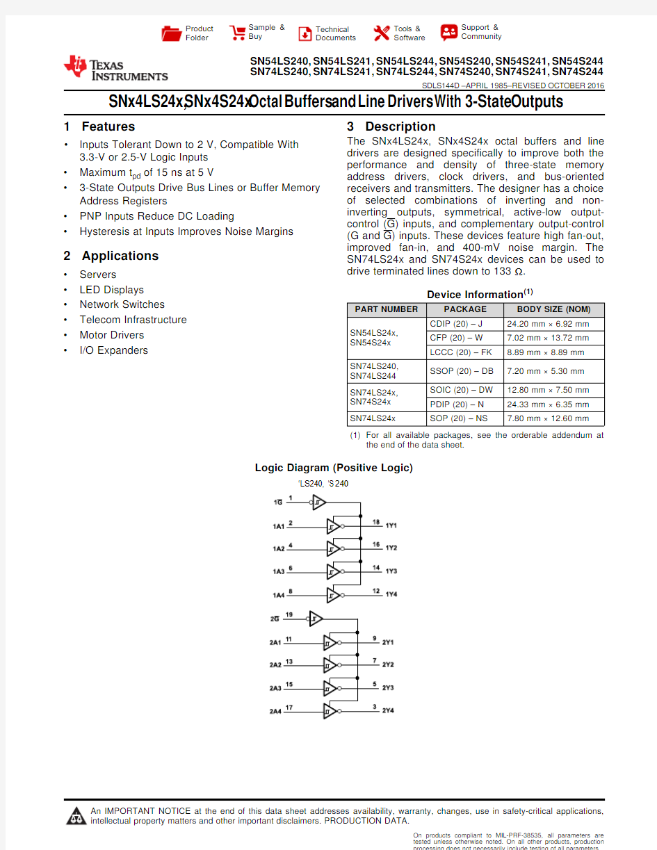
Logic Diagram (Positive Logic)
万联芯城https://www.doczj.com/doc/8f6648129.html,-电子元器件采购网,提供一站式配套,解决物料烦恼,万联芯城销售电子元器件范围包括IC集成电路,电阻电容,二三极管,可进行一站式BOM表配单,BOM配单采购可节省逐个搜索购买环节,只需提交BOM物料清单,商城即可为您报价,为客户节省采购成本,满足客户物料需求,点击进入万联芯城。
2SN54LS240,SN54LS241,SN54LS244,SN54S240,SN54S241,SN54S244SN74LS240,SN74LS241,SN74LS244,SN74S240,SN74S241,SN74S244
SDLS144D –APRIL 1985–REVISED OCTOBER https://www.doczj.com/doc/8f6648129.html,
Submit Documentation Feedback Copyright ?1985–2016,Texas Instruments Incorporated
Table of Contents
1
Features (12)
Applications (13)
Description (14)
Revision History (25)
Pin Configuration and Functions .........................36Specifications .........................................................
46.1
Absolute Maximum Ratings......................................46.2
ESD Ratings..............................................................46.3
Recommended Operating Conditions.......................46.4
Thermal Information .................................................56.5
Electrical Characteristics –SNx4LS24x....................56.6
Electrical Characteristics –SNx4S24x......................56.7
Switching Characteristics –SNx4LS24x...................66.8
Switching Characteristics –SNx4S24x.....................66.9Typical Characteristics..............................................77Parameter Measurement Information ..................77.1SN54LS24x and SN74LS24x Devices. (7)
7.2SN54S24x and SN74S24x Devices (9)
8Detailed Description (11)
8.1Overview.................................................................118.2Functional Block Diagrams.....................................118.3Feature Description.................................................128.4Device Functional Modes........................................129Application and Implementation ........................149.1Application Information............................................149.2Typical Application..................................................149.3System Examples...................................................1510Power Supply Recommendations .....................1711Layout ...................................................................1711.1Layout Guidelines.................................................1711.2Layout Example....................................................1712Device and Documentation Support .................1812.1Related Links........................................................1812.2Receiving Notification of Documentation Updates 1812.3
Community Resource............................................1812.4
Trademarks...........................................................1812.5
Electrostatic Discharge Caution............................1812.6Glossary................................................................1813Mechanical,Packaging,and Orderable Information .. (19)
4Revision History
NOTE:Page numbers for previous revisions may differ from page numbers in the current version.
Changes from Revision C (May 2010)to Revision D
Page ?Added Applications section,ESD Ratings table,Feature Description section,Device Functional Modes ,Application
and Implementation section,Power Supply Recommendations section,Layout section,Device and Documentation
Support section,and Mechanical,Packaging,and Orderable Information section (1)
?Deleted Ordering Information table;see POA at the end of the data sheet (1)
?
Changed R θJA values in the Thermal Information table from 70to 94.3(DB),from 58to 90.3(DW),from 69to 50.6
(N),and from 60to 76.6(NS) (5)
1A22Y31A32Y21A42Y 1G N D 2A 11Y 4
2A 21Y32A31Y22A41Y1G /2G
V C C G 1A 12Y 41G
V CC 1A1
2G/2G 2Y4
1Y11A2
2A42Y3
1Y21A3
2A32Y2
1Y31A4
2A22Y1
1Y4GND 2A13
SN54LS240,SN54LS241,SN54LS244,SN54S240,SN54S241,SN54S244SN74LS240,SN74LS241,SN74LS244,SN74S240,SN74S241,SN74S244
https://www.doczj.com/doc/8f6648129.html, SDLS144D –APRIL 1985–REVISED OCTOBER 2016
Submit Documentation Feedback Copyright ?1985–2016,Texas Instruments Incorporated 5Pin Configuration and Functions
DB,DW,J,N,NS,or W Package
20-Pin SSOP,SOIC,CDIP,PDIP,SOP,or CFP
Top View FK Package 20-Pin LCCC Top View
(1)2G for SNx4LS241and SNx4S241or 2G for all other drivers.
Pin Functions
PIN
I/O DESCRIPTION NO.
NAME 1
1G I Channel 1output enable 2
1A1I Channel 1,A side 13
2Y4O Channel 2,Y side 44
1A2I Channel 1,A side 25
2Y3O Channel 2,Y side 36
1A3I Channel 1,A side 37
2Y2O Channel 2,Y side 28
1A4I Channel 1,A side 49
2Y1O Channel 2,Y side 110
GND —Ground 11
2A1I Channel 2,A side 112
1Y4O Channel 1,Y side 413
2A2I Channel 2,A side 214
1Y3O Channel 1,Y side 315
2A3I Channel 2,A side 316
1Y2O Channel 1,Y side 217
2A4I Channel 2,A side 418
1Y1O Channel 1,Y side 119
2G/2G (1)I Channel 2output enable 20
V CC —Power supply
4SN54LS240,SN54LS241,SN54LS244,SN54S240,SN54S241,SN54S244SN74LS240,SN74LS241,SN74LS244,SN74S240,SN74S241,SN74S244
SDLS144D –APRIL 1985–REVISED OCTOBER https://www.doczj.com/doc/8f6648129.html,
Submit Documentation Feedback Copyright ?1985–2016,Texas Instruments Incorporated
(1)
Stresses beyond those listed under Absolute Maximum Ratings may cause permanent damage to the device.These are stress ratings only,which do not imply functional operation of the device at these or any other conditions beyond those indicated under Recommended Operating Conditions .Exposure to absolute-maximum-rated conditions for extended periods may affect device reliability.(2)Voltage values are with respect to network ground terminal.
6Specifications
6.1Absolute Maximum Ratings
over operating free-air temperature range (unless otherwise noted)(1)
MIN
MAX UNIT Supply voltage,V CC (2)
7V Input voltage,V I
SNx4LS24x 7V SNx4S24x 5.5Off-state output voltage
5.5V Storage temperature,T stg
–65150°C (1)
JEDEC document JEP155states that 500-V HBM allows safe manufacturing with a standard ESD control process.(2)JEDEC document JEP157states that 250-V CDM allows safe manufacturing with a standard ESD control process.
6.2ESD Ratings
VALUE
UNIT ALL PACKAGES
V (ESD)
Electrostatic discharge Human-body model (HBM),per ANSI/ESDA/JEDEC JS-001(1)500V N PACKAGE V (ESD)
Electrostatic discharge Charged device model (CDM),per JEDEC specification JESD22-C101(2)500V (1)
Voltage values are with respect to network ground terminal.(2)An SN54S241J operating at free-air temperature above 116°C requires a heat sink that provides a thermal resistance from case to free
air,R θCA ,of not more that 40°C/W.
6.3Recommended Operating Conditions
over operating free-air temperature range (unless otherwise noted)
MIN
NOM MAX UNIT V CC
Supply voltage (1)SN54xS24x 4.55 5.5V SN74xS24x 4.755 5.25V IH
High-level input voltage 2V V IL
Low-level input voltage SN54LS24x 0.7V SN54S24x,SN74xS24x 0.8I OH High-level output current SN54xS24x
–12mA SN74xS24x
–15I OL Low-level output current SN54LS24x
12mA SN54S24x
48SN74LS24x
24SN74S24x
64External resistance between any input and V CC or ground (SNx4S24x only)
40k ΩT A
Operating free-air temperature (2)SN54xS24x –55125°C SN74xS24x 070
5SN54LS240,SN54LS241,SN54LS244,SN54S240,SN54S241,SN54S244SN74LS240,SN74LS241,SN74LS244,SN74S240,SN74S241,SN74S244
https://www.doczj.com/doc/8f6648129.html, SDLS144D –APRIL 1985–REVISED OCTOBER 2016
Submit Documentation Feedback Copyright ?1985–2016,Texas Instruments Incorporated
(1)
For more information about traditional and new thermal metrics,see the Semiconductor and IC Package Thermal Metrics application report.(2)
Voltage values are with respect to network ground terminal.(3)The package thermal impedance is calculated in accordance with JESD 51-7.
6.4Thermal Information
THERMAL METRIC (1)SN74LS240,SN74LS244SN74LS24x,SN74S24x SN74LS24x UNIT DB (SSOP)
DW (SOIC)N (PDIP)NS (SOP)20PINS
20PINS 20PINS 20PINS R θJA
Junction-to-ambient thermal resistance (2)(3)94.390.350.676.6°C/W R θJC(top)
Junction-to-case (top)thermal resistance 55.945.537.442.9°C/W R θJB
Junction-to-board thermal resistance 49.548.131.544.1°C/W ψJT
Junction-to-top characterization parameter 21.319.42419.2°C/W ψJB
Junction-to-board characterization parameter 49.147.631.443.7°C/W (1)
For conditions shown as minimum or maximum,use the appropriate value specified under recommended operating conditions.(2)
All typical values are at V CC =5V and T A =25°C.
(3)Not more than one output must be shorted at a time,and duration of the short-circuit must not exceed one second.
6.5Electrical Characteristics –SNx4LS24x
over recommended operating free-air temperature range (unless otherwise noted)
PARAMETER
TEST CONDITIONS (1)MIN TYP (2)MAX UNIT V IK
V CC =MIN,I I =–18mA –1.5V Hysteresis
(V T+?V T ?)
V CC =MIN 0.20.4V V OH
V CC =MIN,I OH =–3mA,V IH =2V,V IL =MAX 2.4 3.4V V CC =MIN,I OH =MAX,V IH =2V,V IL =0.5V 2V OL
V CC =MIN,V IL =MAX,V IH =2V I OL =12mA,SN54LS24x 0.4V I OL =24mA,SN74LS24x 0.5I OZH
V CC =MAX,V IL =MAX,V IH =2V,V O =2.7V 20μA I OZL
V CC =MAX,V IL =MAX,V IH =2V,V O =0.4V –20μA I I
V CC =MAX,V I =7V 0.1mA I IH
V CC =MAX,V I =2.7V 20μA I IL
V CC =MAX,V IL =0.4V –0.2mA I OS (3)V CC =MAX
–40–225mA I CC V CC =MAX,output open Outputs high
All 1727mA Outputs low
SNx4LS2402644SNx4LS241,SNx4LS2442746Outputs disabled
SNx4LS2402950SNx4LS241,SNx4LS2443254(1)
For conditions shown as minimum or maximum,use the appropriate value specified under recommended operating conditions.(2)All typical values are at V CC =5V,T A =25°C.
6.6Electrical Characteristics –SNx4S24x
over recommended operating free-air temperature range (unless otherwise noted)
PARAMETER
TEST CONDITIONS (1)MIN TYP (2)MAX UNIT V IK
V CC =MIN,I I =–18mA –1.2V Hysteresis
(V T+?V T ?)
V CC =MIN 0.20.4V V OH
V CC =MIN,I OH =–1mA,V IH =2V,V IL =0.8V,SN74S24x only 2.7V V CC =MIN,I OH =–3mA,V IH =2V,V IL =0.8V 2.4 3.4V CC =MIN,I OH =MAX,V IH =2V,V IL =0.5V 2V OL
V CC =MIN,V IL =MAX,V IH =2V,I OL =0.8V 0.55V
6SN54LS240,SN54LS241,SN54LS244,SN54S240,SN54S241,SN54S244SN74LS240,SN74LS241,SN74LS244,SN74S240,SN74S241,SN74S244
SDLS144D –APRIL 1985–REVISED OCTOBER https://www.doczj.com/doc/8f6648129.html,
Submit Documentation Feedback Copyright ?1985–2016,Texas Instruments Incorporated
Electrical Characteristics –SNx4S24x (continued)
over recommended operating free-air temperature range (unless otherwise noted)
PARAMETER
TEST CONDITIONS (1)MIN TYP (2)MAX UNIT (3)Not more than one output must be shorted at a time,and duration of the short-circuit must not exceed one second.
I OZH
V CC =MAX,V IL =0.8V,V IH =2V,V O =2.4V 50μA I OZL
V CC =MAX,V IL =MAX,V IH =2V,V O =0.5V –50μA I I
V CC =MAX,V I =5.5V 1mA I IH
V CC =MAX,V I =2.7V 50μA I IL
V CC =MAX,V IL =0.5V Any A –400μA Any G –2mA I OS (3)V CC =MAX
–50–225mA I CC V CC =MAX,output open Outputs high SN54S240
80123mA SN74S240
80135SN54S241,SN54S244
95147SN74S241,SN74S244
95160Outputs low SN54S240
100145SN74S240
100150SN54S241,SN54S244
120170SN74S241,SN74S244
120180Outputs disabled SN54S240
100145SN74S240
100150SN54S241,SN54S244
120170SN74S241,SN74S244
1201806.7Switching Characteristics –SNx4LS24x
V CC =5V,T A =25°C (see SN54LS24x and SN74LS24x Devices )
PARAMETER
TEST CONDITIONS MIN TYP MAX UNIT t PLH
R L =667Ω,C L =45pF SNx4LS240914ns SNx4LS241,SNx4LS2441218t PHL
R L =667Ω,C L =45pF 1218ns t PZL
R L =667Ω,C L =45pF 2030ns t PZH
R L =667Ω,C L =45pF 1523ns t PLZ
R L =667Ω,C L =5pF 1020ns t PHZ R L =667Ω,C L =5pF 1525ns
6.8Switching Characteristics –SNx4S24x
V CC =5V and T A =25°C (see SN54S24x and SN74S24x Devices )
PARAMETER
TEST CONDITIONS MIN TYP MAX UNIT t PLH
R L =90Ω,C L =50pF SNx4S240 4.57ns SNx4S241,SNx4S24469t PHL
R L =90Ω,C L =50pF SNx4S240 4.57ns SNx4S241,SNx4S24469t PZL
R L =90Ω,C L =50pF 1015ns t PZH
R L =90Ω,C L =50pF SNx4S240 6.510ns SNx4S241,SNx4S244812t PLZ
R L =90Ω,C L =5pF 1015ns t PHZ R L =90Ω,C L =5pF 69ns
V CC
Test Point From Output Under Test
(see Note
High-Level
Pulse Low-Level
Pulse (see Note B)
V CC
From Output Under Test (see Note S1
S2(see Note B)V L From Output Under Test Test
Point 7
SN54LS240,SN54LS241,SN54LS244,SN54S240,SN54S241,SN54S244SN74LS240,SN74LS241,SN74LS244,SN74S240,SN74S241,SN74S244
https://www.doczj.com/doc/8f6648129.html, SDLS144D –APRIL 1985–REVISED OCTOBER 2016
Submit Documentation Feedback Copyright ?1985–2016,Texas Instruments Incorporated 6.9Typical Characteristics
V CC =5V,T A =25°C,C L =45pF,and R L =667Ω(unless otherwise noted)
7Parameter Measurement Information
7.1SN54LS24x and SN74LS24x Devices
Figure 2.Load Circuit,For 2-State Totem-Pole Outputs
Figure 3.Load Circuit,For Open-Collector Outputs Figure 4.Load Circuit,For 3-State Outputs
Figure 5.Voltage Waveforms,Pulse Durations
Output
Control
(low-level
enabling)
Waveform 1
(see Notes C
and D)
Waveform 2
(see Notes C
and D)
V OH 0.3 V –OL + 0.3 V 1.5 V
≈1.5 V
Input Out-of-Phase
Output
(see Note D) 3 V 0 V V OL V OH V OH
V OL
In-Phase Output (see Note D)3 V 3 V 0 V 0 V Timing
Input
Data
Input 8SN54LS240,SN54LS241,SN54LS244,SN54S240,SN54S241,SN54S244SN74LS240,SN74LS241,SN74LS244,SN74S240,SN74S241,SN74S244
SDLS144D –APRIL 1985–REVISED OCTOBER https://www.doczj.com/doc/8f6648129.html,
Submit Documentation Feedback Copyright ?1985–2016,Texas Instruments Incorporated
Figure 6.Voltage Waveforms,Setup and Hold Times
Figure 7.Voltage Waveforms,Propagation Delay Times
A.
C L includes probe and jig capacitance.B.
All diodes are 1N3064or equivalent.C.Waveform 1is for an output with internal conditions such that the output is low except when disabled by the output
control.Waveform 2is for an output with internal conditions such that the output is high except when disabled by the
output control.
D.S1and S2are closed for t PLH ,t PHL ,t PHZ ,and t PLZ ;S1is open and S2is closed for t PZH ;S1is closed and S2is open
for t PZL .
E.Phase relationships between inputs and outputs have been chosen arbitrarily for these examples.
F.All input pulses are supplied by generators having the following characteristics:PRR ≤1MHz,Z O is approximately
50Ω,t r ≤15ns,t f ≤6ns.
G.
The outputs are measured one at a time with one input transition per measurement.Figure 8.Voltage Waveforms,Enable and Disable Times,3-State Outputs
(see Note B)V CC
From Output Under Test (see Note S1S2
Input Out-of-Phase
Output
(see Note D) 3 V
0 V V OL V OH V OH
V OL
In-Phase
Output
(see Note D)
V CC Test Point From Output
Under Test
(see Note 3 V 3 V 0 V 0 V Timing
Input
Data
Input
(see Note B)V L
From Output
Under
Test
Test
High-Level
Pulse Low-Level Pulse 9
SN54LS240,SN54LS241,SN54LS244,SN54S240,SN54S241,SN54S244SN74LS240,SN74LS241,SN74LS244,SN74S240,SN74S241,SN74S244
https://www.doczj.com/doc/8f6648129.html, SDLS144D –APRIL 1985–REVISED OCTOBER 2016
Submit Documentation Feedback Copyright ?1985–2016,Texas Instruments Incorporated 7.2SN54S24x and SN74S24x Devices
Figure 9.Load Circuit,For 2-State Totem-Pole Outputs Figure 10.Load Circuit,For Open-Collector Outputs Figure 11.Load Circuit,For 3-State Outputs
Figure 12.Voltage Waveforms,Pulse Durations
Figure 13.Voltage Waveforms,Setup and Hold Times Figure 14.Voltage Waveforms,Propagation Delay Times
3 V
0 V
Output
Control
(low-level
enabling)
Waveform1
(see Notes C
and D)
Waveform2
(see Notes C
and D)
≈1.5 V
V OH?0.5 V
V OL+ 0.5 V
≈1.5 V
10
SN54LS240,SN54LS241,SN54LS244,SN54S240,SN54S241,SN54S244
SN74LS240,SN74LS241,SN74LS244,SN74S240,SN74S241,SN74S244
SDLS144D–APRIL1985–REVISED https://www.doczj.com/doc/8f6648129.html, Submit Documentation Feedback Copyright?1985–2016,Texas Instruments Incorporated
A.C L includes probe and jig capacitance.
B.All diodes are1N3064or equivalent.
C.Waveform1is for an output with internal conditions such that the output is low except when disabled by the output
control.Waveform2is for an output with internal conditions such that the output is high except when disabled by the
output control.
D.S1and S2are closed for t PLH,t PHL,t PHZ,and t PLZ;S1is open and S2is closed for t PZH;S1is closed and S2is open
for t PZL.
E.All input pulses are supplied by generators having the following characteristics:PRR≤1MHz,Z O is approximately
50Ω;t r and t f≤7ns for SN54LS24x and SN74LS24x devices,and t r and t f≤2.5ns for SN54S24x and SN74S24x
devices.
F.The outputs are measured one at a time with one input transition per measurement.
Figure15.Voltage Waveforms,
Enable and Disable Times,3-State Outputs
2Y1
2Y2
2Y3
2Y4
2G
1G
Copyright ? 2016,Texas Instruments Incorporated
1Y1
1Y2
1Y3
1Y4
Copyright ? 2016,Texas Instruments Incorporated 11
SN54LS240,SN54LS241,SN54LS244,SN54S240,SN54S241,SN54S244SN74LS240,SN74LS241,SN74LS244,SN74S240,SN74S241,SN74S244
https://www.doczj.com/doc/8f6648129.html, SDLS144D –APRIL 1985–REVISED OCTOBER 2016
Submit Documentation Feedback Copyright ?1985–2016,Texas Instruments Incorporated 8Detailed Description
8.1Overview
This device is organized as two 4-bit buffers and drivers with separate output-enable (G)inputs.When G is low,
the device passes data from the A inputs to the Y outputs.When G is high,the outputs are in the high
impedance state.Inputs can be driven from either 3.3-V or 5-V devices.This feature allows the use of this device
as a translator in a mixed 3.3-V and 5-V system environment.To ensure the high-impedance state during power
up or power down,G must be tied to V CC through a pullup resistor;the minimum value of the resistor is
determined by the current-sinking capability of the driver.
8.2Functional Block Diagrams
Pin numbers shown are for DB,DW,J,N,
NS,and W packages Figure 16.SNx4LS240and SNx4S240Logic Diagram Pin numbers shown are for DB,DW,J,N,
NS,and W packages
Figure 17.SNx4LS241and SNx4S241Logic Diagram
1Y1
1Y2
1Y3
1Y4
Copyright ? 2016,Texas Instruments Incorporated
12SN54LS240,SN54LS241,SN54LS244,SN54S240,SN54S241,SN54S244SN74LS240,SN74LS241,SN74LS244,SN74S240,SN74S241,SN74S244
SDLS144D –APRIL 1985–REVISED OCTOBER https://www.doczj.com/doc/8f6648129.html,
Submit Documentation Feedback Copyright ?1985–2016,Texas Instruments Incorporated
Pin numbers shown are for DB,DW,J,N,NS,and W packages
Figure 18.SNx4LS244and SNx4S244Logic Diagram
8.3Feature Description
8.3.13-State Outputs
The 3-state outputs can drive bus lines directly.All outputs can be put into high impedance mode through the G
pin.
8.3.2PNP Inputs
This device has PNP inputs which reduce dc loading on bus lines.
8.3.3Hysteresis on Bus Inputs
The bus inputs have built-in hysteresis that improves noise margins.
8.4Device Functional Modes
The SNx4LS24x and SNx4S24x devices can be used as inverting and non-inverting bus buffers for data line
transmission and can isolate input to output by setting the G pin HIGH.Table 1,Table 2,and Table 3list the
function tables for all devices.
Table 1.SNx4LS240and SNx4S240Function Table
INPUTS
OUTPUTS G
A Y L
L H L
H L H
X Z
V CC
Input
Copyright ? 2016,Texas Instruments Incorporated
V CC
Output
GND
Copyright ? 2016,Texas Instruments Incorporated
Input
Copyright ? 2016,Texas Instruments Incorporated 13
SN54LS240,SN54LS241,SN54LS244,SN54S240,SN54S241,SN54S244SN74LS240,SN74LS241,SN74LS244,SN74S240,SN74S241,SN74S244
https://www.doczj.com/doc/8f6648129.html, SDLS144D –APRIL 1985–REVISED OCTOBER 2016
Submit Documentation Feedback Copyright ?1985–2016,Texas Instruments Incorporated Table 2.SNx4LS241and SNx4S241Function Table
CHANNEL 1
CHANNEL 2INPUTS
OUTPUT INPUTS OUTPUT 1G
1A 1Y 2G 2A 2Y L
L L H L L L
H H H H H H X Z L X Z
Table 3.SNx4LS244and SNx4S244Function Table
INPUTS
OUTPUTS G
A Y L
L L L
H H H X Z
Figure 19.SNx4LS240,SNx4LS241,SNx4LS244Equivalent of Each Input
G and G inputs:R eq =2k ΩNOM
A inputs:R eq =2.8k ΩNOM
Figure 20.SNx4S240,SNx4S241,SNx4S244Equivalent of Each Input
SNx4LS240,SNx4LS241,SNx4LS244:R =50ΩNOM
SNx4S240,SNx4S241,SNx4S244:
R =25ΩNOM
Figure 21.Typical of All Outputs
Copyright ? 2016,Texas Instruments Incorporated
14SN54LS240,SN54LS241,SN54LS244,SN54S240,SN54S241,SN54S244SN74LS240,SN74LS241,SN74LS244,SN74S240,SN74S241,SN74S244
SDLS144D –APRIL 1985–REVISED OCTOBER https://www.doczj.com/doc/8f6648129.html,
Submit Documentation Feedback Copyright ?1985–2016,Texas Instruments Incorporated
9Application and Implementation
NOTE
Information in the following applications sections is not part of the TI component
specification,and TI does not warrant its accuracy or completeness.TI’s customers are
responsible for determining suitability of components for their purposes.Customers should
validate and test their design implementation to confirm system functionality.
9.1Application Information
The SNx4LS24x,SNx4S24x octal buffers and line drivers are designed to be used for a multitude of bus
interface type applications where output drive or PCB trace length is a concern.
9.2Typical Application
Figure 22.SNx4LS241and SNx4S241Used as Repeater or Level Restorer
9.2.1Design Requirements
This device uses Schottky transistor logic technology.Take care to avoid bus contention because it can drive
currents that would exceed maximum limits.The high drive creates fast edges into light loads,so routing and
load conditions must be considered to prevent ringing.
9.2.2Detailed Design Procedure
?Power Supply
–Each device must maintain a supply voltage between 4.5V and 5.5V.
?Inputs
–Input signals must meet the V IH and V IL specifications in Electrical Characteristics –SNx4LS24x .
–Inputs leakage values (I I ,I IH ,I IL )from Electrical Characteristics –SNx4LS24x must be considered.
?Outputs
–Output signals are specified to meet the V OH and V OL specifications in Electrical Characteristics –
SNx4LS24x as a minimum (the values could be closer to V CC for high signals or GND for low signals).
–TI recommends maintaining output currents as specified in Recommended Operating Conditions .
–The part can be damaged by sourcing or sinking too much current (see Electrical Characteristics –
SNx4LS24x for details).
Copyright ? 2016,Texas Instruments Incorporated
I OL (mA)V OL
(max)V 03691215
18212427
0.2
0.4
15
SN54LS240,SN54LS241,SN54LS244,SN54S240,SN54S241,SN54S244SN74LS240,SN74LS241,SN74LS244,SN74S240,SN74S241,SN74S244
https://www.doczj.com/doc/8f6648129.html, SDLS144D –APRIL 1985–REVISED OCTOBER 2016
Submit Documentation Feedback Copyright ?1985–2016,Texas Instruments Incorporated Typical Application (continued)
9.2.3Application Curve
Figure 23.V OL vs I OL
9.3System Examples
The SNx4LS240and SNx4S240devices can be used to buffer signals along a memory bus.The increased
output drive helps data transmission reliability.Figure 24shows a schematic of this example.
4-bit organization can be applied to handle binary or BCD
Figure 24.SNx4LS240and SNx4S240Used as System or Memory Bus Driver
The SNx4LS240and SNx4S240devices have two independently controlled 4-bit drivers,and can be used to
buffer signals in a bidirectional manner along a data bus.Figure 25shows the SNx4LS240or SNx4S240used in
this manner.
Input A
To Other
Buffers
Output A
Control
H
H
L
L
H H L L H L Input Output Control B B A A None 1/4 'LS241/'S241
Party-Line Multiple-Input/Output Bus 1/4 'LS241/'S241Input B To Other Buffers Output B
A B B A None L H H L L L L H H H
Copyright ? 2016,Texas Instruments Incorporated
Copyright ? 2016,Texas Instruments Incorporated
16SN54LS240,SN54LS241,SN54LS244,SN54S240,SN54S241,SN54S244SN74LS240,SN74LS241,SN74LS244,SN74S240,SN74S241,SN74S244
SDLS144D –APRIL 1985–REVISED OCTOBER https://www.doczj.com/doc/8f6648129.html,
Submit Documentation Feedback Copyright ?1985–2016,Texas Instruments Incorporated
System Examples (continued)
Figure 25.Independent 4-Bit But Drivers/Receivers in a Single Package
The enable pins on the SNx4LS241and SNx4S241devices can be used to help direct signals along a shared
party-line bus.Figure 26shows a general configuration of how to implement this structure.Take care to ensure
that bus contention does not occur.
Figure 26.Party-Line Bus System With Multiple Inputs,Outputs,and Receivers
V CC
Input Output Output
Input 17
SN54LS240,SN54LS241,SN54LS244,SN54S240,SN54S241,SN54S244SN74LS240,SN74LS241,SN74LS244,SN74S240,SN74S241,SN74S244
https://www.doczj.com/doc/8f6648129.html, SDLS144D –APRIL 1985–REVISED OCTOBER 2016
Submit Documentation Feedback Copyright ?1985–2016,Texas Instruments Incorporated 10Power Supply Recommendations
The power supply can be any voltage between the minimum and maximum supply voltage rating located in
Recommended Operating Conditions .Each V CC pin must have a good bypass capacitor to prevent power
disturbance.For devices with a single supply,TI recommends a 0.1-μF bypass capacitor.If there are multiple
V CC pins,TI recommends a 0.01-μF or 0.022-μF bypass capacitors for each power pin.It is acceptable to parallel
multiple bypass capacitors to reject different frequencies of noise.Two bypass capacitors of value 0.1μF and
1μF are commonly used in parallel.For best results,install the bypass capacitor(s)as close to the power pin as
possible.
11Layout
11.1Layout Guidelines
When using multiple bit logic devices,inputs must not be left floating.In many applications,some channels of the
SNx4LS24x,SNx4S24x are unused,and thus must be terminated properly.Because each transceiver channel
pin can be either an input or an output,they must be treated as both when being terminated.Ground or V CC (whichever is more convenient)can be used to terminate unused inputs;however,each unused channel should
be terminated to the same logic level on both the A and Y side.For example,in Figure 27unused channels are
terminated correctly with both sides connected to the same voltage,while channel 8is terminated incorrectly with
each side being tied to a different voltage.The G input is also unused in this example,and is terminated directly
to ground to permanently enable all outputs.
11.2Layout Example
Figure 27.Example Demonstrating How to Terminate Unused Inputs and Channels of a Transceiver
18SN54LS240,SN54LS241,SN54LS244,SN54S240,SN54S241,SN54S244SN74LS240,SN74LS241,SN74LS244,SN74S240,SN74S241,SN74S244
SDLS144D –APRIL 1985–REVISED OCTOBER https://www.doczj.com/doc/8f6648129.html,
Submit Documentation Feedback Copyright ?1985–2016,Texas Instruments Incorporated
12Device and Documentation Support
12.1Related Links
The table below lists quick access links.Categories include technical documents,support and community
resources,tools and software,and quick access to sample or buy.
Table 4.Related Links
PARTS
PRODUCT FOLDER SAMPLE &BUY TECHNICAL DOCUMENTS SUPPORT &COMMUNITY SN54LS240
Click here Click here Click here Click here SN74LS241
Click here Click here Click here Click here SN74LS244
Click here Click here Click here Click here SN54S240
Click here Click here Click here Click here SN54S241
Click here Click here Click here Click here SN54S244
Click here Click here Click here Click here SN74LS240
Click here Click here Click here Click here SN74LS241
Click here Click here Click here Click here SN74LS244
Click here Click here Click here Click here SN74S240
Click here Click here Click here Click here SN74S241
Click here Click here Click here Click here SN74S241Click here Click here Click here Click here
12.2Receiving Notification of Documentation Updates
To receive notification of documentation updates,navigate to the device product folder on https://www.doczj.com/doc/8f6648129.html,.In the upper
right corner,click on Alert me to register and receive a weekly digest of any product information that has
changed.For change details,review the revision history included in any revised document.
12.3Community Resource
The following links connect to TI community resources.Linked contents are provided "AS IS"by the respective
contributors.They do not constitute TI specifications and do not necessarily reflect TI's views;see TI's Terms of
Use .
TI E2E?Online Community TI's Engineer-to-Engineer (E2E)Community.Created to foster collaboration
among engineers.At https://www.doczj.com/doc/8f6648129.html,,you can ask questions,share knowledge,explore ideas and help
solve problems with fellow engineers.
Design Support TI's Design Support Quickly find helpful E2E forums along with design support tools and
contact information for technical support.
12.4Trademarks
E2E is a trademark of Texas Instruments.
All other trademarks are the property of their respective owners.
12.5Electrostatic Discharge Caution
These devices have limited built-in ESD protection.The leads should be shorted together or the device placed in conductive foam
during storage or handling to prevent electrostatic damage to the MOS gates.
12.6Glossary
SLYZ022—TI Glossary .
This glossary lists and explains terms,acronyms,and definitions.
19
SN54LS240,SN54LS241,SN54LS244,SN54S240,SN54S241,SN54S244SN74LS240,SN74LS241,SN74LS244,SN74S240,SN74S241,SN74S244
https://www.doczj.com/doc/8f6648129.html, SDLS144D –APRIL 1985–REVISED OCTOBER 2016
Submit Documentation Feedback Copyright ?1985–2016,Texas Instruments Incorporated 13Mechanical,Packaging,and Orderable Information
The following pages include mechanical,packaging,and orderable information.This information is the most
current data available for the designated devices.This data is subject to change without notice and revision of
this document.For browser-based versions of this data sheet,refer to the left-hand navigation.