±50ppb超高精度温度补偿晶振
- 格式:pdf
- 大小:299.90 KB
- 文档页数:1
晶振简介(OCXO恒温、 MCXO数补、VCXO压控、VCTCXO、VCOCXO)各种晶振简介1. 普通晶振Packaged Crystal Oscillator(PXO):是⼀种没有采取温度补偿措施的晶体振荡器,在整个温度范围内,晶振的频率稳定度取决于其内部所⽤晶体的性能,频率稳定度在10-5量级,⼀般⽤于普通场所作为本振源或中间信号,是晶振中最廉价的产品。
2. 温补晶振Temperature Compensated Crystal Oscillator(TCXO):是在晶振内部采取了对晶体频率温度特性进⾏补偿,以达到在宽温温度范围内满⾜稳定度要求的晶体振荡器。
⼀般模拟式温补晶振采⽤热敏补偿⽹络。
补偿后频率稳定度在10-7~10-6量级,由于其良好的开机特性、优越的性能价格⽐及功耗低、体积⼩、环境适应性较强等多⽅⾯优点,因⽽获⾏了⼴泛应⽤。
3. 压控晶振Voltage Controlled Crystal Oscillator(VCXO):是⼀种可通过调整外加电压使晶振输出频率随之改变的晶体振荡器,主要⽤于锁相环路或频率微调。
压控晶振的频率控制范围及线性度主要取决于电路所⽤变容⼆极管及晶体参数两者的组合 4. 恒温晶振Oven Controlled Crystal Oscillator(OCXO):采⽤精密控温,使电路元件及晶体⼯作在晶体的零温度系数点的温度上。
中精度产品频率稳定度为10-7~10-8,⾼精度产品频率稳定度在10-9量级以上。
主要⽤作频率源或标准信号 5. 电压控制-温补晶体振荡器(VCTCXO)温度补偿晶体振荡器和电压控制晶体振荡器结合。
6. 电压控制-恒温晶体振荡器(VCOCXO)恒温晶体振荡器和电压控制晶体振荡器结合。
晶振的应⽤:晶体振荡器被⼴泛应⽤到军、民⽤通信电台,微波通信设备,程控电话交换机,⽆线电综合测试仪,BP机、移动电话发射台,⾼档频率计数器、GPS、卫星通信、遥控移动设备等。
热敏晶振温度补偿算法你知道吗,热敏晶振其实就像是我们人类的“体温计”,不过它测的可不是人的体温,而是温度对晶体振荡频率的影响。
哎,说到这,你可能会好奇,温度和频率到底有啥关系呢?晶振就像是我们大脑的“钟表”,它工作的时候,是通过一个非常精确的频率来保持系统的稳定运转。
但是一旦温度变化,晶振的频率就像放风筝一样,控制不住,飞得偏了。
这时候,我们就需要温度补偿算法来帮忙,确保晶振在各种温度下都能稳稳地“报时”。
所以啊,咱们今天就来聊聊这个神奇的热敏晶振温度补偿算法,嗯,大家不用担心,咱们不讲什么艰深的公式,保证让你轻松懂。
其实热敏晶振温度补偿就是为了应对温度变化对晶振频率的影响。
有些晶振就很“娇气”,温度一高一低,它的“心情”就跟着变化。
你想想,温度一变,频率也随之“跳舞”,根本没办法维持在一个稳定的水平。
补偿算法就像是给晶振开了一张温度调整的“处方”,让它在不同温度下都能保持稳定,像是给它穿上了“防寒服”和“防晒衣”,不管外面温度怎么变,它都能安安稳稳地工作。
怎么补偿呢?很简单,补偿的原则就是通过一个特定的算法,精确地计算出温度变化对频率的影响,然后反向调整,使得频率始终保持在一个我们希望的数值范围内。
听起来是不是很神奇?但实际上,做到这一点并不容易,尤其是当温度变化幅度很大时,补偿的精度要求就会非常高。
这时,不少小伙伴就会想了:“哎呀,这种算法难不难啊?我是不是要去学好多数学?”放心,没那么复杂。
其实就像我们日常生活中调味料一样,掌握了比例,就能做出好吃的菜肴。
补偿算法就是通过对晶振在不同温度下的频率特性进行数据分析,得出一个数学模型。
然后,系统就能根据实时的温度变化,调整晶振的工作状态,做到“温度不改频率”的目标。
简单来说,就是温度和频率之间的关系早就被“摸透了”,然后再根据这个规律,做出一些微调。
就像你调整音响的音量,虽然听不见细微的变化,但声音就好听多了。
再说了,为什么这个补偿算法这么重要呢?你想啊,现在咱们用的电子设备无论是手机、电脑还是智能家居,都会依赖于高精度的晶振来保持系统的同步。
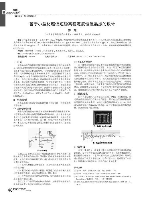
• 92•描述了一种新型恒温晶振(OCXO)的设计方案,在恒温晶振(OCXO)研究基础上,通过对控温电路的优化设计,并采用热敏网络补偿技术,以恒温控制为主,温度补偿为辅,先进行恒温控制,再进行温度补偿。
两者相互结合取得优良的温频特性。
新型恒温晶振的工作电压仅为5V。
其温度-频率特性及相位噪声分别达到≤±1ppb(-40~+70℃)和≤-158dBc/Hz@1kHz的指标。
稳态功耗仅为1.2W,体积为36*27*12.7mm。
引言:石英晶体振荡器是无线电设备的核心部件,是通信、广播、雷达、电子对抗、遥控遥测及许多测量仪器必不可少的部件,其中恒温晶体振荡器(OCXO )是一种频率稳定性最好的高精密晶体振荡器(蒋松涛,一种小型超低相噪恒温晶振的设计:压电与声光,2015)。
大量应用于高端通讯设备中。
目前温频特性要达到10-9~10-11数量级普遍采用双层恒温技术。
存在预热时间长,体积大,功耗高等缺点(赵声衡,晶体振荡器:科学出版社,2008)。
本文描述了一种恒温控制为主,温度补偿为辅,两者相结合的新型OCXO 设计方案。
并成功研制了体积为36×27×12.7(mm ),温度稳定度优于±1×10⁻⁹的小体积低功耗恒温晶振。
1 晶体谐振器温频特性晶体谐振器是一种基于压电效应实现的机械振动系统。
其晶片切型有很多种,包括AT 切、SC 切、BT 切等。
其中比较常用、生产较成熟的是AT 切和SC 切。
SC 切谐振器的显著特点是其频率与温度之间有近似的三次函数关系,因而它具有零温度系数点(John R.Vig Quartz Crystal Resonators and Oscillators For Frequency Control and Timing Applications:U.S.Army Communications-Electronics Command,2001)。
2400 Series-square wave in 25.4x25.4mm DIP packageNA-10M-2400 series oscillators are designed for applications where space is at apremium and good frequency stability is required. The oscillators can be used in many communications applications. A choice of quartz resonators offers a variety of performance versus cost options to fit most applications.ELECTRICAL SPECIFICA TIONS1.OUTPUT (PIN = “R.F. OUTPUT”)ParameterMin. Typ.Max. UnitTest Condition1.1.Frequency10.000000MHz1.2.Initial Accuracy -0.1 +0.1 ppm@ +25 ±1°Cafter turn on power 15 ±1 minutes ≤ 90 days following date code VCO Input at Center Voltage ±0.001V1.3. Waveform Rectangular 1.4.LevelLVTTL “1” level +2.6 +3.3 V “0” level +0.4 V1.5. Load 15 pF1.6. Duty cycle 45 50 55 % @ +1.65V 1.7. Rise/fall time 6 ns 10% to 90% 1.8.Spurious-60dBc2.FREQUENCY STABILITYParameterMin. Typ.Max. UnitTest Condition2.1.Ambient ±3, ±5, ±10 ppb referenced to 25°C Refer to Table 1 : Ordering Information-30 ~ +70 -40 ~ +85°C2.2.Aging-0.5+0.5 ppb per day, at time of shipment Daily -0.5 +0.5 ppb after 30 days Yearly -50 +50 ppb 10 Years-0.3 +0.3 ppm2.3. Voltage -0.5 +0.5 ppb ±5% change 2.4. Short term 0.05 ppb/s root Allan variance 2.5. Load -0.5 +0.5 ppb ±5% change2.6. Warm-up -10 +10 ppb in 10 minutes @ +25 ±1°C referenced to 1 hourRoHS Compliant StandardRev(1)09/2014深圳捷比信--高品质精密元件供应商www.jepsun.comParameter Min. Typ. Max. Unit Test Condition2.7. Phase Noise-95 -90 dBc/Hz @ 1Hz (@25°C)-125 -120 dBc/Hz @ 10Hz (@25°C)-140 -135 dBc/Hz @ 100Hz (@25°C) -148 -145 dBc/Hz @ 1KHz (@25°C) -156 -155 dBc/Hz @ 10KHz (@25°C) -158 -155 dBc/Hz @ 100KHz (@25°C)3. ELECTRICAL FREQUENCY ADJUSTMENT (PIN = “VCO INPUT”)Parameter Min. Typ. Max. Unit Test Condition3.1. Tuning Range-0.5 ppm ***************Referenced to frequency at nominalCenter Voltage+0.5 ppm ***************3.2. Control Voltage 0 +5.0 VOptional, Refer to Table 1 : Ordering Information 0 +4.0 V3.3. Slope Positive3.4. Center Voltage +2.5 VOptional, Refer to Table 1 : Ordering Information Note 1 +2.0 V3.5. Linearity -10 +10 %3.6. Input Impedance 100 kΩ4. INPUT POWER (PIN = “+VDC”)Parameter Min. Typ. Max. Unit Test Condition4.1. Voltage +4.75 +5.0 +5.25 V4.2. Current 800 mA @ turn on4.3. Steady State 1.3 W @ +25°C5. REFERENCE VOLTAGE (PIN = "REFERENCE VOLTAGE")(Optional Function. Refer to Table 1 : Ordering Information.)Parameter Min. Typ. Max. Units Test Condition5.1. Voltage +3.8 +4 +4.2 V Over temperature range in 2.1.5.2. Load 9 kΩ6. ENVIRONMENTALParameter Reference Std. Test Condition6.1. Operating Temperature -40°C to +85°C Note 26.2. Storage Temperature-55°C to +105°C6.3. Humidity MIL-STD-202, Method 103Test Condition A 95% RH @ +40°C,non-condensing,240 hours6.4. Vibration (non-operating) MIL-STD-202, Method 201 0.06” Total p-p, 10 to 55 Hz6.5. Shock (non-operating) MIL-STD-202, Method 213,Test Condition J30g, 11ms, half-sineNote 1. When not connected, VCO INPUT is internally held at this voltage.Note 2. Output maintained over this temperature range. Other requirements of this specification may not be met when operating outside the temperature range in 2.1.Rev(1)09/2014深圳捷比信--高品质精密元件供应商www.jepsun.comOUTLINE DRA WINGTable 1 : ORDERING INFORMA TIONRev(1)09/2014 深圳捷比信--高品质精密元件供应商www.jepsun.com。
晶振电路的生产研发条件质量保证命名规则恒温晶体振荡器(OCXOs)OX253B-H-MR-V-10M OX362D-H-MR-V-10MOX20系列10~40SC±0.01~0.20.2S/T/HOX30x系列10~120SC±0.005~0.20.5S/T/H-140/-14556●●9●1215订购表7●OX14B-T-HU-V-10MOX12A-T-HT-V-40M温度补偿晶体振荡器(TCXOs)TX12/TX14/TX15系列10~120±0.5~512/5/3.3S/T/H/CTXG36B-S-KW-R@300M1922命名规则●-55~+85CTX7A-C-GU-V@10M TX12B-T-JW-N@20M注:ppm=10,120MHz以上为倍频输出,可选定制产品;10MHz以下为分频输出;产品概览8●型号频率范围f(MHz)频率温度稳定度压控频率范围工作电压V输出选择*电压控制晶体振荡器(VCXOs)ppmVX12/VX14/VXM14(SMD)ppm压控线性注:ppm=10, 除VXM15系列外,频率>35MHz压控频率范围为±30ppm; 需宽压控频率范围可选倍频输出。
*:S:Sinewave; LC:L VCMOS; LP:LVPECL。
VXM15B-T-HQ-A@100M页码24命名规则●VX12/VX14/VXM14集成晶体振荡器目录封装外形尺寸图35(TMs )±ppmppm时钟模块概述VTM18B-T-HT-001页码TM18系列±4.62/2CMOS5/3.328±0.370.008~32.768●27集成晶体振荡器目录(XTALs )封装页码29命名规则●±5ppm1、完善的晶体谐振器生产线2 我们拥有1000m 资上千万元完整的晶体谐振器生产线,其主要设备从国外引进,可生产高Q、低老化冷压焊和电阻焊(抽真空)SC、AT切晶体。
晶振的精度参数详解以晶振的精度参数详解为题,我们将详细介绍晶振的精度参数,包括频率精度和稳定度。
一、频率精度:晶振的频率精度是指晶振输出的频率与其标称频率之间的差异。
频率精度通常以ppm(百万分之一)或ppb(十亿分之一)为单位进行表示。
频率精度越高,晶振输出的频率与标称频率的差异越小,晶振的性能越好。
频率精度受到多种因素的影响,主要包括晶振的制造工艺、晶体材料的质量以及外部环境的温度和压力等。
制造工艺的不同会导致晶振的频率精度有所差异,而晶体材料的质量也会直接影响晶振的频率稳定性。
二、稳定度:晶振的稳定度是指晶振输出频率在一定时间范围内的变化程度。
稳定度通常以ppm为单位进行表示。
稳定度越高,晶振的频率变化越小,晶振的性能越好。
稳定度受到多种因素的影响,主要包括晶振的温度特性、老化效应以及外部环境的温度和压力等。
晶振的温度特性是指晶振频率随温度变化的规律,一般情况下,晶振频率会随温度的升高而增加。
晶振的老化效应是指晶振的频率在长时间使用过程中会发生变化,通常情况下,晶振的频率会随时间的推移而逐渐降低。
为了提高晶振的频率精度和稳定度,制造商通常会采用一些技术手段。
例如,采用高精度的晶体材料、优化晶振的制造工艺、加入温度补偿电路等。
这些技术手段可以有效地提高晶振的性能,使其在各种应用场景下都能够稳定可靠地工作。
总结起来,晶振的精度参数包括频率精度和稳定度。
频率精度是指晶振输出的频率与其标称频率之间的差异,而稳定度是指晶振输出频率在一定时间范围内的变化程度。
这些参数对于晶振的性能至关重要,制造商通常会通过优化晶振的制造工艺和采用一些技术手段来提高晶振的频率精度和稳定度。
只有在频率精度和稳定度都达到要求的情况下,晶振才能在各种应用场景下稳定可靠地工作。
rtc温度补偿补偿晶振的精度1. 引言RTC(Real-Time Clock)是一种能够提供准确时间和日期信息的电子设备。
而晶振是RTC中的重要组成部分,负责提供稳定的时钟信号。
然而,晶振的频率会受到温度的影响而发生变化,从而影响RTC的准确性。
因此,为了提高RTC的精度,需要进行温度补偿。
2. 温度对晶振的影响温度会导致晶振的频率发生变化,主要原因是晶体的物理性质会随温度变化而改变。
一般来说,温度升高会导致晶体的振荡频率增加,温度降低则会使振荡频率减小。
这种频率变化对于RTC来说是不可忽视的,因为即使温度仅变化几度,晶振频率的变化也可能导致RTC的时间计算错误。
3. RTC温度补偿原理RTC温度补偿是通过测量环境温度并根据温度变化来调整晶振频率,从而实现对晶振精度的补偿。
一般来说,RTC温度补偿分为两个步骤:温度测量和频率补偿。
(1) 温度测量:通过传感器等设备测量环境温度,获取当前温度值。
(2) 频率补偿:根据温度的变化,计算需要补偿的频率值,并通过控制电路对晶振频率进行调整。
4. RTC温度补偿的应用RTC温度补偿广泛应用于需要高精度时间计算的领域,例如航空航天、通信设备、工业自动化等。
在这些领域中,时间的准确性对于系统的正常运行至关重要。
通过RTC温度补偿,可以提高系统的时间精度,减少时间误差,提高系统的可靠性和稳定性。
5. RTC温度补偿的实现RTC温度补偿的实现需要依赖精确的温度传感器、控制电路和补偿算法。
常见的温度传感器包括热敏电阻、温度传感器芯片等,用于测量环境温度。
控制电路则根据测量到的温度值计算需要补偿的频率值,并通过控制晶振的振荡电路对晶振频率进行调整。
补偿算法可以根据具体的应用需求进行设计,常见的有线性补偿、多项式补偿等。
6. RTC温度补偿的挑战与改进RTC温度补偿在实际应用中还面临一些挑战。
首先,温度传感器的精度和稳定性对补偿效果有重要影响,需要选择合适的传感器以确保温度测量的准确性。
32.768khz 温补晶振电路
32.768kHz温补晶振电路通常由一个晶体振荡器和一些辅助元件组成,其目的是为了稳定地提供32.768kHz的时钟信号。
这个信号广泛应用于各种数字集成电路中,如实时时钟(RTC)等,作为计时基准。
以下是一个基本的32.768kHz温补晶振电路的组成部分:
1. 晶体:核心元件是石英晶体,它具有非常高的Q值,可以产生3
2.768kHz 的振荡频率。
2. 反相器:通常采用CMOS反相器,它为晶体提供偏置,使晶体工作在饱和区,以获得较大的增益。
3. 负载电容:C1和C2是晶体的负载电容,与反相器一起形成一个负阻,为晶体提供振荡所需的能量。
4. 温度补偿电容:C3和C4是温度补偿电容,通常连接到晶体的两个端子,以稳定其振荡频率。
5. 电阻:R1和R2是电阻,用于降低对晶体的驱动能量,防止晶体振坏或出现异常。
6. 反相器:inv2对invl的输出波形进行整形并驱动负载。
在实际应用中,为了确保32.768kHz温补晶振电路的稳定性,通常需要接上一个电容来稳定其振荡频率。
这是因为石英晶体的振荡频率受到外界环境温度、机械振动等因素的影响,容易发生波动和漂移。
通过加入一个适当的电容,可以形成一个谐振回路,使得晶振的振荡频率在一定范围内保持稳定。
此外,32.768kHz温补晶振电路具有体积小、功耗低等优点,被广泛应用于各种小型电子设备中,如腕表、电子计时器、温度计、LCD屏幕驱动器等的时钟电路中。
频率偏差ppmppb晶振,全称晶体振荡器,它能够产⽣中央处理器(CPU)执⾏指令所必须要的时钟频率信号,CPU⼀切指令的执⾏都是建⽴在这个基础上的,时钟信号频率越⾼,通常CPU的运⾏速度也就越快。
晶振有⼏个重要参数:1,晶体元件规格书中所指定的频率,也是⼯程师在电路设计和元件选购时⾸要关注的参数。
晶振常⽤标称频率在1~200MHz之间,⽐如32768Hz、8MHz、12MHz、24MHz、125MHz等,更⾼的输出频率也常⽤PLL(锁相环)将低频进⾏倍频⾄1GHz以上。
我们称之为标称频率。
2,输出信号的频率不可避免会有⼀定的偏差,我们⽤频率误差(Frequency Tolerance)或频率稳定度(Frequency Stability),⽤单位ppm来表⽰,即百万分之⼀(parts per million)(1/10^6),是相对标称频率的变化量,此值越⼩表⽰精度越⾼。
⽐如,12MHz晶振偏差为±20ppm,表⽰它的频率偏差为12×20Hz=±240Hz,即频率范围是(11999760~12000240Hz)3,还有⼀个温度频差(Frequency Stability vs Temp)表⽰在特定温度范围内,⼯作频率相对于基准温度时⼯作频率的允许偏离,它的单位也是ppm。
4,另外,负载电容CL(Load capacitance),它是电路中跨接晶体两端的总的有效电容(不是晶振外接的匹配电容),主要影响负载谐振频率和等效负载谐振电阻,与晶体⼀起决定振荡器电路的⼯作频率,通过调整负载电容,就可以将振荡器的⼯作频率微调到标称值。
更准确⽽⾔,⽆源晶体的负载电容是⼀项⾮常重要的参数,因为⽆源晶体属于被动元器件,所谓的被动元器件即是⾃⾝不能⼯作,需要外部元器件协助⼯作,⽆源晶体即是!其中:CS为晶体两个管脚之间的寄⽣电容(⼜名晶振静态电容或Shunt Capacitance),在晶体的规格书上可以找到具体值,⼀般0.2pF~8pF不等。
晶振常用的精度表示方法
晶振是一种常见的电子元件,用于产生稳定的时钟信号,广泛应用于各种电子设备和系统中。
为了确保设备的正常运行,晶振的精度非常重要。
而精度表示方法可以通过以下几种方式实现:
1. 频率精度:晶振的频率精度通常以频率偏差来表示。
偏差值越小,表示晶振的频率越准确。
一般使用单位为ppm(百万分之一)或ppb(十亿分之一)来表示偏差。
例如,某个晶振的频率精度为±10ppm,意味着其频率偏差在所设定的频率值上下波动不超过10ppm。
2. 温度精度:晶振的工作稳定性受温度的影响较大,因此温度精度是评估晶振性能的重要指标之一。
通常使用单位为ppm/℃(百万分之一/摄氏度)来表示温度精度。
例如,某个晶振的温度精度为±5ppm/℃,意味着在每升高1摄氏度的温度变化下,其频率偏差不超过5ppm。
3. 长期稳定性:晶振的长期稳定性指的是在长时间运行过程中,其频率偏差的变化程度。
一般使用年平均频率偏差(Annual Average Deviation, AAD)来表示长期稳定性。
例如,某个晶振的长期稳定性为±1ppm,意味着在一年的运行时间内,其频率偏差不超过1ppm。
除了以上几种常用的精度表示方法外,还有其他一些方式也可用于描述晶振的精度,如相位噪声、功率供应稳定性等。
根据不同的应用需求,晶振的精度表示方法可以选择适合的指标进行评估和比较,以确保设备或系统的高可靠性和稳定性。
SiT53561 – 60 MHz, ±0.1 to ±0.25 ppm, Stratum 3, Elite Platform™ Precision Super-TCXODescriptionThe SiT5356 is a ±100 ppb precision MEMS Super-TCXO that is fully compliant to Telcordia GR-1244-CORE Stratum 3 oscillator specifications. Engineered for best dynamic performance, the SiT5356 is ideal for high reliability telecom, wireless and networking, industrial, precision GNSS and audio/video applications.L everaging SiTime’s unique DualMEMS™ temperature sensi ng and TurboCompensation™ technolog ies, the SiT5356 delivers the best dynamic performance for timing stability in the presence of environmental stressors due to air flow, temperature perturbation, vibration, shock, and electromagnetic interference. This device also integrates multiple on-chip regulators to filter power supply noise, eliminating the need for a dedicated external LDO.The SiT5356 offers three device configurations that can be ordered using Ordering Codes for:1)TCXO with non-pullable output frequency,2)VCTCXO allowing voltage control of outputfrequency, and3)DCTCXO, enabling digital control of output frequencyusing an I2C interface, pullable to 5 ppt (parts pertrillion) resolution.The SiT5356 can be factory programmed for any combination of frequency, stability, voltage, and pull range. Programmability enables designers to optimize clock configurations while eliminating long lead times and customization costs associated with quartz devices where each frequency is custom built.Refer to Manufacturing Guideline for proper reflow profile and PCB cleaning recommendations to ensure best performance. Features⏹Any frequency from 1 MHz to 60 MHz in 1 Hz steps ⏹Factory programmable options for low lead time⏹Best dynamic stability under airflow, thermal shock▪±100 ppb stability across temperature▪±1 ppb/ C typical frequency slope (ΔF/ΔT)▪3e-11 ADEV at 10 second averaging time⏹-40°C to +105°C operating temperature⏹No activity dips or micro jumps⏹Resistant to shock, vibration and board bending⏹On-chip regulators eliminate the need for external LDOs ⏹Digital frequency pulling (DCTCXO) via I2C▪Digital control of output frequency and pull range ▪Up to ±3200 ppm pull range▪Frequency pull resolution down to 5 ppt⏹ 2.5V, 2.8V, 3.0V and 3.3V supply voltage⏹LVCMOS or clipped sinewave output⏹RoHS and REACH compliant⏹Pb-free, Halogen-free, Antimony-free Applications⏹4G/5G radio, Small cell⏹IEEE1588 boundary and grandmaster clocks⏹Carrier-grade routers and switches⏹Synchronous Ethernet⏹Optical transport – SONET/SDH, OTN, Stratum 3⏹DOCSIS 3.x remote PHY⏹GPS disciplined oscillators⏹Precision GNSS systems⏹Test and measurementBlock DiagramFigure 1. SiT5356 Block Diagram 5.0 x 3.2 mm2 Package PinoutOE / VC / NC12345678910SCL / NCNCGNDNCNCVDDCLKA0 / NCSDA / NCFigure 2. Pin Assignments (Top view) (Refer to Table 13for Pin Descriptions)Ordering InformationThe following part number guide is for reference only. To customize and build an exact part number, use theSiTime Part Number Generator. To validate the part number, use the SiTime Part Number Decoder.Notes:1. “-“ corresponds to the default rise/fall time for LVCMOS output as specified in Table 1 (Electrical Characteristics). Contact SiTime for other rise/fall time optionsfor best EMI.2. Bulk is available for sampling onlyTABLE OF CONTENTSDescription (1)Features (1)Applications (1)Block Diagram (1)5.0 x 3.2 mm2 Package Pinout (1)Ordering Information (2)Electrical Characteristics (4)Device Configurations and Pin-outs (10)Pin-out Top Views (10)Test Circuit Diagrams for LVCMOS and Clipped Sinewave Outputs (11)Waveforms (13)Timing Diagrams (14)Typical Performance Plots (15)Architecture Overview (19)Frequency Stability (19)Output Frequency and Format (19)Output Frequency Tuning (19)Pin 1 Configuration (OE, VC, or NC) (20)Device Configurations (20)TCXO Configuration (20)VCTCXO Configuration (21)DCTCXO Configuration (22)VCTCXO-Specific Design Considerations (23)Linearity (23)Control Voltage Bandwidth (23)FV Characteristic Slope K V (23)Pull Range, Absolute Pull Range (24)DCTCXO-Specific Design Considerations (25)Pull Range and Absolute Pull Range (25)Output Frequency (26)I2C Control Registers (28)Register Descriptions (28)Register Address: 0x00. Digital Frequency Control Least Significant Word (LSW) (28)Register Address: 0x01. OE Control, Digital Frequency Control Most Significant Word (MSW) (29)Register Address: 0x02. DIGITAL PULL RANGE CONTROL[14] (30)Serial Interface Configuration Description (31)Serial Signal Format (31)Parallel Signal Format (32)Parallel Data Format (32)I2C Timing Specification (34)I2C Device Address Modes (35)Schematic Example (36)Dimensions and Patterns (37)Layout Guidelines (38)Manufacturing Guidelines (38)Electrical CharacteristicsAll Min and Max limits are specified over temperature and rated operating voltage with 15 pF output load unless otherwise stated. Typical values are at 25°C and 3.3V Vdd.Table 1. Output CharacteristicsTable 1. Output Characteristics (continued)Table 2. DC CharacteristicsTable 3. Input CharacteristicsNote:3. APR = PR – initial tolerance – 20-year aging – frequency stability over temperature. Refer to Table 17 for APR with respect to other pull range options.Table 5. Jitter & Phase Noise – Clipped Sinewave, -40 to 85 °CTable 7. Jitter & Phase Noise – Clipped Sinewave, -40 to 105 °CTable 8. Absolute Maximum LimitsAttempted operation outside the absolute maximum ratings may cause permanent damage to the part.Actual performance of the IC is only guaranteed within the operational specifications, not at absolute maximum ratings.Note:4. Exceeding this temperature for an extended period of time may damage the device.Table 9. Thermal Considerations[5]Note:5. Measured in still air.Table 10. Maximum Operating Junction Temperature[6]Note:6. Datasheet specifications are not guaranteed if junction temperature exceeds the maximum operating junction temperature.Table 11. Environmental ComplianceDevice Configurations and Pin-outsTable 12. Device ConfigurationsPin-out Top ViewsOE/NC12345678910NC NC GNDNC NC VDD CLKNCNCFigure 3. TCXOVC 12345678910NC NC GNDNC NC VDD CLKNCNCFigure 4. VCTCXOOE / NC 12345678910 SCL NC GNDNC NC VDD CLKA0 / NCSDAFigure 5. DCTCXOTable 13. Pin DescriptionNotes:7. In OE mode for noisy environments, a pull-up resistor of 10 kΩ or less is recommended if pin 1 is not externally driven. If pin 1 needs to be left floating, use the NC option.8. A 0.1 μF capacitor in parallel with a 10 μF capacitor are required between Vdd and GND. The 0.1 μF capacitor is recommended to place close to the device, and place the 10 μF capacitor less than 2 inches away.9. All NC pins can be left floating and do not need to be soldered down.Test Circuit Diagrams for LVCMOS and Clipped Sinewave OutputsFigure 6. LVCMOS Test Circuit (OE Function)Figure 7. Clipped Sinewave Test Circuit (OE Function)for AC and DC MeasurementsVC FunctionFigure 8. LVCMOS Test Circuit (VC Function)VC FunctionFigure 9. Clipped Sinewave Test Circuit (VC Function)for AC and DC MeasurementsNC FunctionFigure 10. LVCMOS Test Circuit (NC Function)NC FunctionFigure 11. Clipped Sinewave Test Circuit (NC Function)for AC and DC MeasurementsTest Circuit Diagrams for LVCMOS and Clipped Sinewave Outputs (continued)FunctionFigure 12. LVCMOS Test Circuit (I2C Control), DCTCXO modeFunction2C Control), DCTCXO mode for AC and DC MeasurementsFigure 13. Clipped Sinewave Test Circuit (IFigure 14. Clipped Sinewave Test Circuit for Phase Noise Measurements, Applies to All Configurations(NC Function shown for example only)Note:10.SDA is open-drain and may require pull-up resistor if not present in I2C test setup.Waveforms90 % Vdd 50 % Vdd10 % VddFigure 15. LVCMOS Waveform Diagram[11]Figure 16. Clipped Sinewave Waveform Diagram[11]Note:11.Duty Cycle is computed as Duty Cycle = TH/Period.Timing DiagramsVdd Pin CLK OutputT_start: Time to start from power-offFigure 17. Startup Timing T_oe: Time to re-enable the clock outputFigure 18. OE Enable Timing (OE Mode Only)Typical Performance PlotsFigure 19. ADEV (±0.1 ppm)Figure 20. TDEV (0.1 Hz loop bandwidth, ±0.1 ppm)Figure 21. MTIE (0.1 Hz loop bandwidth, ±0.1 ppm)Figure 22. Frequency vs Temperature (±0.1 ppm), 105°CFigure 23. Freq. vs. Temp. Slope (ΔF/ΔT), ±0.1 ppm deviceFigure 24. VCTCXO frequency pull characteristicFigure 25. 1-day aging rate (to 62 days), ±0.1 ppm deviceFigure 26. Drift over 30 days relative to the first readingTypical Performance Plots (continued)Figure 27. Load sensitivity (±0.1 ppm )Figure 28. VDD sensitivity (±0.1 ppm)Figure 31. IDD TCXO (LVCMOS)Figure 32. IDD VCTCXO (LVCMOS)Figure 33. T_phj, RMS Random, (DC)TCXO (LVCMOS)Figure 34. Period Jitter, RMS (LVCMOS)Figure 35. IDD DCTCXO (LVCMOS)Figure 36. T_phj, RMS Random, VCTCXO (LVCMOS)Figure 37. DCTCXO frequency pull characteristicFigure 38. Rise Time (Clipped Sinewave)Figure 39. IDD TCXO (Clipped Sinewave)Figure 40. IDD VCTCXO (Clipped Sinewave)Figure 41. T_phj, RMS Random, (DC)TCXO (Clipped Sine)Figure 42. IDD DCTCXO (Clipped Sinewave)Figure 43. T_phj, RMS Random, VCTCXO (Clipped Sine)Figure 44. Duty Cycle (Clipped Sinewave)Architecture OverviewBased on SiTime’s innovative Elite Platform™, the SiT5356 delivers exceptional dynamic performance, i.e. resilience to environmental stressors such as shock, vibration, and fast temperature transients. Underpinning the Elite platform are SiTime’s unique DualMEMS™temperature sensing architecture and TurboCompensation™ technologies. DualMEMS is a noiseless temperature compensation scheme. It consists of two MEMS resonators fabricated on the same die substrate. The TempFlat™resonator is designed with a flat frequency characteristic over temperature whereas the temperature sensing resonator is by design sensitive to temperature changes. The ratio of frequencies between these two resonators provides an accurate reading of the resonator temperature with 20 µK resolution.By placing the two MEMS resonators on the same die, this temperature sensing scheme eliminates any thermal lag and gradients between resonator and temperature sensor, thereby overcoming an inherent weakness of legacy quartz TCXOs.The DualMEMS temperature sensor drives a state-of-the-art CMOS temperature compensation circuit. The TurboCompensation design, with >100 Hz compensation bandwidth, achieves a dynamic frequency stability that is far superior to any quartz TCXO. The digital temperature compensation enables additional optimization of frequency stability and frequency slope over temperature within any chosen temperature range for a given system design.Figure 45. Elite ArchitectureThe Elite platform also incorporates a high resolution, low noise frequency synthesizer along with the industry standard I2C bus. This unique combination enables system designers to digitally control the output frequency in steps as low as 5 ppt and over a wide range up to ±3200 ppm. For more information regarding the Elite platform and its benefits please visit:⏹SiTime's breakthroughs section⏹TechPaper:DualMEMS Temperature Sensing Technology ⏹TechPaper:DualMEMS Resonator TDC Functional OverviewThe SiT5356 is designed for maximum flexibility with an array of factory programmable options, enabling system designers to configure this precision device for optimal performance in a given application.Frequency StabilityThe SiT5356 comes in two factory-trimmed stability grades that are optimized for different applications. Both Stratum 3+ and Stratum 3 devices are compliant with Stratum 3 stability of ±4.6 ppm over 20 years.Table 14. Stability Grades vs. Ordering Codes⏹Stratum 3+ grade with ΔF/ΔT of ±3.5 ppb/︒C isengineered to provide significantly better performancethan legacy quartz TCXOs in time and phasesynchronization applications such as IEEE1588, smallcells, and 5G C-RAN (cloud RAN).⏹Stratum 3 grade is designed to replace classicStratum 3 TCXOs in applications such as SyncE withbetter dynamic performance and shorter lead time. Output Frequency and FormatThe SiT5356 can be factory programmed for an outputfrequency without sacrificing lead time or incurring an upfront customization cost typically associated with custom-frequency quartz TCXOs.The device supports both LVCMOS and clipped sinewave output. Ordering codes for the output format are shown below: Table 15. Output Formats vs. Ordering CodesOutput Frequency TuningIn addition to the non-pullable TCXO, the SiT5356 can also support output frequency tuning through either an analog control voltage (VCTCXO), or I2C interface (DCTCXO). The I2C interface enables 16 factory programmed pull-range options from ±6.25 ppm to ±3200 ppm. The pull range can also be reprogrammed via I2C to any supported pull-range value.Refer to Device Configuration section for details.Pin 1 Configuration (OE, VC, or NC)Pin 1 of the SiT5356 can be factory programmed to support three modes: Output Enable (OE), Voltage Control (VC), or No Connect (NC).Table 16. Pin Configuration OptionsWhen pin 1 is configured as OE pin, the device output is guaranteed to operate in one of the following two states:⏹Clock output with the frequency specified in the partnumber when Pin 1 is pulled to logic high⏹Hi-Z mode with weak pull down when pin 1 is pulled tologic low.When pin 1 is configured as NC, the device is guaranteed to output the frequency specified in the part number at all times, regardless of the logic level on pin 1.In the VCTCXO configuration, the user can fine-tune the output frequency from the nominal frequency specified in the part number by varying the pin 1 voltage. The guaranteed allowable variation of the output frequency is specified as pull range. A VCTCXO part number must contain a valid pull-range ordering code. Device ConfigurationsThe SiT5356 supports 3 device configurations –TCXO,VCTCXO, and DCTCXO. The TCXO and VCTCXO options are directly compatible with the quartz TCXO and VCTCXO. The DCTCXO configuration provides performance enhancement by eliminating VCTCXO’s sensitivity to control voltage noise with an I2C digital interface for frequency tuning.Figure 46. Block Diagram – TCXOTCXO ConfigurationThe TCXO configuration generates a fixed frequency output, as shown in Figure 46. The frequency is specified by the user in the frequency field of the device ordering code and then factory programmed. Other factory programmable options include supply voltage, output types (LVCMOS or clipped sinewave), and pin 1 functionality (OE or NC).Refer to the Ordering Information section at the end of the datasheet for a list of all ordering options.A VCTCXO, shown in Figure 47, is a frequency control device whose output frequency is an approximately linear function of control voltage applied to the voltage control pin. VCTCXOs have a number of use cases including the VCO portion of a jitter attenuation/jitter cleaner PLL Loop.The SiT5356 achieves a 10x better pull range linearity of <0.5% via a high-resolution fractional PLL compared with 5% to 10% typical of quartz VCTCXOs that rely on pulling a resonator. By contrast, quartz-based VCTCXOs change output frequency by varying the capacitive load of a crystal resonator using varactor diodes, which results in poor linearity.Figure 47. Block Diagram – VCTCXO Note that the output frequency of the VCTCXO is proportional to the analog control voltage applied to pin 1. Because this control signal is analog and directly controls the output frequency, care must be taken to minimize noise on this pin.The nominal output frequency is factory programmed per the customer’s request to 6 digits of precision and is defined as the output frequency when the control voltage equals Vdd/2. The maximum output frequency variation from this nominal value is set by the pull range, which is also factory programmed to the customer’s desired value and specified by the ordering code. The Ordering Information section shows all ordering options and associated ordering codes. Refer to VCTCXO-Specific Design Considerations for more information on critical VCTCXO parameters including pull range linearity, absolute pull range,control voltage bandwidth, and Kv.The SiT5356 offers digital control of the output frequency, as shown in Figure 48. The output frequency is controlled by writing frequency control words over the I2C interface. There are several advantages of DCTCXOs relative to VCTCXOs:1)Frequency control resolution as low as 5 ppt. Thishigh resolution minimizes accumulated time error insynchronization applications.2)Lower system cost – A VCTCXO may need a Digital toAnalog Converter (DAC) to drive the control voltageinput. In a DCTXCO, the frequency control is achieveddigitally by register writes to the control registers viaI2C, thereby eliminating the need for a DAC.3)Better noise immunity –The analog signal used todrive the voltage control pin of a VCTCXO can besensitive to noise, and the trace over which the signalis routed can be susceptible to noise coupling from thesystem. The DCTCXO does not suffer from analognoise coupling since the frequency control isperformed digitally through I2C.Figure 48. Block Diagram4)No frequency-pull non-linearity – The frequency pullingis achieved via fractional feedback divider of the PLL, eliminating any pull non-linearity concerns typical of quartz-based VCTCXOs. This improves dynamic performance in closed-loop applications.5)Programmable wide pull range –The DCTCXOpulling mechanism is via the fractional feedback divider and is therefore not constrained by resonator pullability as in quartz-based solutions. The SiT5356 offers 16 frequency pull-range options from ±6.25ppm to ±3200ppm, providing system designers great flexibility.Refer to DCTCXO-Specific Design Considerations for more information on critical DCTCXO parameters including pull range, absolute pull range, frequency output, and I2Ccontrol registers.VCTCXO-Specific Design ConsiderationsLinearityIn any VCTCXO, there will be some deviation of the frequency-voltage (FV) characteristic from an ideal straight line. Linearity is the ratio of this maximum deviation to the total pull range, expressed as a percentage. Figure 49 below shows the typical pull linearity of a SiTime VCTCXO. The linearity is excellent (1% maximum) relative to most quartz offerings because the frequency pulling is achieved with a PLL rather than varactor diodes.Figure 49. Typical SiTime VCTCXO LinearityControl Voltage BandwidthControl voltage b andwidth, sometimes called “modulation r ate” or “modulation b andwidth”, indicates how fast a VCO can respond to voltage changes at its input. The ratio of the output frequency variation to the input voltage variation, previously denoted by K V, has a low-pass characteristic in most VCTCXOs. The control voltage bandwidth equals the modulating frequency where the output frequency deviation equals 0.707 (e.g. -3 dB) of its DC value, for DC inputs swept in the same voltage range.For example, a part with a ±6.25 ppm pull range and a 0-3V control voltage can be regarded as having an average KV of 4.17 ppm/V (12.5 ppm/3V = 4.17 ppm/V). Applying an input of 1.5V DC ± 0.5V (1.0 V to 2.0V) causes an output frequency change of 4.17 ppm (±2.08 ppm). If the control voltage bandwidth is specified as 10 kHz, the peak-to-peak value of the output frequency change will be reduced to 4.33 ppm/√2 or 2.95 ppm, as the frequency of the control voltage change is increased to 10 kHz.FV Characteristic Slope K VThe slope of the FV characteristic is a critical design parameter in many low bandwidth PLL applications. The slope is the derivative of the FV characteristic –the deviation of frequency divided by the control voltage change needed to produce that frequency deviation, over a small voltage span, as shown below:inoutV VfK∆∆=It is typically expressed in kHz/Volt, MHz/Volt, ppm/Volt, or similar units. This s lope is usually called “K V” based on terminology used in PLL designs.The extreme linear characteristic of the SiTime SiT5356 VCTCXO family means that there is very little K V variation across the whole input voltage range (typically <1%), significantly reducing the design burden on the PLL designer. Figure50below illustrates the typical K V variation.Figure 50. Typical SiTime K V VariationPull Range, Absolute Pull RangePull range (PR) is the amount of frequency deviation that will result from changing the control voltage over its maximum range under nominal conditions.Absolute pull range (APR) is the guaranteed controllable frequency range over all environmental and aging conditions. Effectively, it is the amount of pull range remaining after taking into account frequency stability, tolerances over variables such as temperature, power supply voltage, and aging, i.e.:agingstability F F PR APR --=where stability F is the device frequency stability due to initial tolerance and variations on temperature, power supply, and load.Figure 51 shows a typical SiTime VCTCXO FV characteristic. The FV characteristic varies with conditions, so that the frequency output at a given input voltage can vary by as much as the specified frequency stability of the VCTCXO. For such VCTCXOs, the frequency stability and APR are independent of each other. This allows very wide range of pull options without compromising frequency stability.Figure 51. Typical SiTime VCTCXO FV Characteristic The upper and lower control voltages are the specified limits of the input voltage range as shown in Figure 51 above. Applying voltages beyond the upper and lower voltages do not result in noticeable changes of output frequency. In other words, the FV characteristic of the VCTCXO saturates beyond these voltages. Figures 1 and 2 show these voltages as Lower Control Voltage (VC_L) and Upper Control Voltage (VC_U).Table 17 below shows the pull range and corresponding APR values for each of the frequency vs. temperature ordering options.Table 17. VCTCXO Pull Range, APR Options [12] Typical unless specified otherwise. Pull range (PR) is ±6.25 ppm.Notes:12.APR includes initial tolerance, frequency stability vs. temperature, and the corresponding 20-year aging.DCTCXO-Specific Design ConsiderationsPull Range and Absolute Pull RangePull range and absolute pull range are described in theprevious section. Table 18 below shows the pull range andcorresponding APR values for each of the frequency vs.temperature ordering options.Table 18. APR Options[13]Notes:13.APR includes initial tolerance, frequency stability vs. temperature, and the corresponding 20-year aging.Output FrequencyThe device powers up at the nominal operating frequency and pull range specified by the ordering code. After power-up both pull range and output frequency can be controlled via I2C writes to the respective control registers. The maximum output frequency change is constrained by the pull range limits.The pull range is specified by the value loaded in the digital pull-range control register. The 16 pull range choices are specified in the control register and range from ±6.25ppm to ±3200ppm.Table 19 below shows the frequency resolution versus pull range programmed valueTable 19. Frequency Resolution versus Pull RangeThe ppm frequency offset is specified by the 26 bit DCXO frequency control register in two’s complement format as described in the I2C Register Descriptions. The power up default value is 00000000000000000000000000b which sets the output frequency at its nominal value (0 ppm). To change the output frequency, a frequency control word is written to 0x00[15:0] (Least Significant Word) and 0x01[9:0] (Most Significant Word). The LSW value should be written first followed by the MSW value; the frequency change is initiated after the MSW value is written.Figure 52. Pull Range and Frequency Control WordFigure 52shows how the two’s complement signed value of the frequency control word sets the output frequency within the ppm pull range set by 0x02:[3:0]. This example shows use of the ±200 ppm pull range. Therefore, to set the desired output frequency, one just needs to calculate the fraction of full scale value ppm, con vert to two’s complement binary, and then write these values to the frequency control registers.The following formula generates the control word value: Control word value = RND((225-1) × ppm shift from nominal/pull range), where RND is the rounding function which rounds the number to the nearest whole number. Two examples follow, assuming a ±200 ppm pull range: Example 1:⏹Default Output Frequency = 19.2 MHz⏹Desired Output Frequency = 19.201728 MHz (+90 ppm) 225-1 corresponds to +200 ppm, and the fractional value required for +90 ppm can be calculated as follows.⏹90 ppm / 200 ppm × (225-1) = 15,099,493.95.Rounding to the nearest whole number yields 15,099,494 and converting to two’s complement gives a binary value of 111001100110011001100110, or E66666 in hex.Example 2:⏹Default Output Frequency = 10 MHz⏹Desired Output Frequency = 9.998 MHz (-50 ppm) Following the formula shown above,⏹(-50 ppm / 200 ppm) × (225-1) = -8,388,607.75. Rounding this to the nearest whole number results in-8,388,608.Converting this to two’s complement binary results in 11100000000000000000000000, or 3800000 in hex. To summarize, the procedure for calculating the frequency control word associated with a given ppm offset is as follows:1)Calculate the fraction of the half-pull range needed.For example, if the total pull range is set for ±100 ppmand a +20 ppm shift from the nominal frequency isneeded, this fraction is 20 ppm/100 ppm = 0.22)Multiply this fraction by the full-half scale word value,225-1 = 33,554,431, round to the nearest wholenumber, and convert the result to two’s complementbinary. Following the +20ppm example, this value is0.2 × 33,554,431 = 6,710,886.2 and rounded to6,710,886.3)Write the two’s complement binary value starting withthe Least Significant Word (LSW) 0x00[16:0],followed by the Most Significant Word (MSW),0x01[9:0]. If the user desires that the output remainsenabled while changing the frequency, a 1 must alsobe written to the OE control bit 0x01[10] if the devicehas software OE Control Enabled.It is important to note that the maximum Digital Control update rate is 38 kHz regardless of I2C bus speed.I2C Control RegistersThe SiT5356 enables control of frequency pull range, frequency pull value, and Output Enable via I2C writes to the control registers. Table 20 below shows the register map summary, and detailed register descriptions follow.Table 20. Register Map SummaryRegister DescriptionsRegister Address: 0x00. Digital Frequency Control Least Significant Word (LSW)。
数字补偿温补晶振工作原理
嘿!今天咱们来聊聊数字补偿温补晶振的工作原理呀!这可真是个有趣又重要的话题呢!
哎呀呀,你知道吗?数字补偿温补晶振在现代电子设备中那可是起着至关重要的作用哇!那它到底是怎么工作的呢?
首先呀,咱们得明白晶振是啥。
简单来说,晶振就是给电子设备提供稳定频率的“小能手”呢!而数字补偿温补晶振呢,则是在普通晶振的基础上进行了升级和优化。
它的工作原理其实挺神奇的!它会通过内部的传感器来感知环境温度的变化呀!哇,这是不是很厉害?然后呢,根据温度的变化,它会利用数字补偿技术来调整晶振的输出频率。
这就保证了在不同的温度条件下,晶振都能提供稳定准确的频率呢!
你想想,如果没有数字补偿温补晶振,那我们的手机、电脑等电子设备的性能是不是会大打折扣呀?比如说,通信可能会不稳定,数据传输可能会出错。
哎呀呀,那可真是不敢想象!
而且哦,数字补偿温补晶振的精度非常高呢!它能够在很宽的温度范围内保持出色的稳定性。
这对于一些对频率要求极高的应用,比如航空航天、军事通信等领域,那简直是太重要啦!
怎么样?是不是对数字补偿温补晶振的工作原理有了更清楚的了解呀?总之呢,这个小小的晶振可是蕴含着大大的科技力量哇!它让我们的生活变得更加便捷和精彩!。
二颗“高精确度、低功耗、小体积”32.768Khz 温补晶体振荡器TCXO 二颗32.768Khz 温补晶体振荡器TCXO的应用方案 DSK321STD 32.768Khz TCXO是上海唐辉电子有限公司目前面向市场推出的一款小体积、高精确度、低功耗的RTC温度补偿石英晶振。
对于目前兴起的智能穿戴市场以及物联网市场、智能医疗、手持式设备、智慧能源等领域来说,DSK321STD这颗产品给工程师们提供了一个非常不错的参考选择。
以智能穿戴产品为例,一般来说需要两个32.768kHz的参考时钟,一个用于MCU的RTC;一个用于蓝牙芯片的睡眠时钟。
如果使用晶体谐振器则需要采用两颗32.768Khz。
由于DSK321STD是一个时钟石英晶体振荡器,它可以很容易驱动两个负载,体现了该产品的优越性。
DSK321STD 32.768Khz TCXO的优势如下:1、采用数字温度补偿方式2、高精确度+/-5ppm(-40-+85°C)、+/-3.8ppm(-10-+60°C)3、低功耗4、宽工作电压范围(2.0V-5.5V)5、宽工作温度(-40-+105°C)6、小体积封装3.2*2.5mm7、无需防湿包装管理8、符合AEC-Q100标准主要参数如下:DSK321STD 32.768Khz实物图:DSK321STD 32.768Khz温度曲线图:DSK321STD 32.768Khz TCXO从2013年底问世以来,在唐辉电子的大力推广之下,目前已经有诸多典型的应用案例,与一些知名品牌的MCU匹配使用:1、德州仪器TI的 MSP430系列2、意法STmicro的STM32系列3、日本瑞萨Renesas的RL78系列4、 Microchip额PIC18/MCP794xx系列5、 Energy Micro的EFG32系列6、 Fujitsu的MB89xx/MB951xx系列7、 NXPDE LPC11xx系列8、 Freescale的L4x/L5x系列第二颗32.768Khz简介如下。