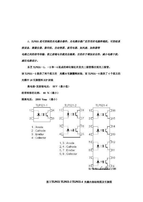
SI8645BC-4路高速光耦
- 格式:pdf
- 大小:509.13 KB
- 文档页数:45

BC846 series65 V, 100 mA NPN general-purpose transistorsRev. 9 — 25 September 2012Product data sheet 1.Product profile1.1General descriptionNPN general-purpose transistors in Surface-Mounted Device(SMD) plastic packages.Table 1.Product overviewType number[1]Package PNP complementN experia JEITA JEDECBC846SOT23-TO-236AB BC856BC846W SOT323SC-70-BC856WBC846T SOT416SC-75-BC856T[1]Valid for all available selection groups.1.2Features and benefits⏹General-purpose transistors⏹SMD plastic packages⏹Two different gain selections1.3Applications⏹General-purpose switching and amplification1.4Quick reference dataTable 2.Quick reference dataSymbol Parameter Conditions Min Typ Max UnitV CEO collector-emitter voltage open base--65VI C collector current--100mAh FE DC current gain V CE=5V; I C=2mA110-450h FE group A110180220h FE group B2002904502.Pinning information3.Ordering information[1]Valid for all available selection groups.4.Marking[1]* = placeholder for manufacturing site codeTable 3.PinningPin Description Simplified outline Graphic symbolSOT23, SOT323, SOT4161base 2emitter 3collector006aaa144123sym02131Table 4.Ordering informationType number [1]Package NameDescriptionVersion BC846-plastic surface-mounted package; 3leads SOT23BC846W SC-70plastic surface-mounted package; 3leads SOT323BC846TSC-75plastic surface-mounted package; 3leadsSOT416Table 5.Marking codesType numberMarking code [1]BC8461D*BC846A 1A*BC846B 1B*BC846W 1D*BC846AW 1A*BC846BW 1B*BC846T 1M BC846AT 1A BC846BT1B5.Limiting values[1]Device mounted on an FR4Printed-Circuit Board (PCB), single-sided copper, tin-plated and standard footprint.6.Thermal characteristics[1]Device mounted on an FR4PCB, single-sided copper, tin-plated and standard footprint.Table 6.Limiting valuesIn accordance with the Absolute Maximum Rating System (IEC 60134).Symbol ParameterConditions Min Max Unit V CBO collector-base voltage open emitter -80V V CEO collector-emitter voltage open base -65V V EBO emitter-base voltage open collector -6V I C collector current -100mA I CM peak collector current single pulse; t p ≤1ms -200mA I BM peak base current single pulse; t p ≤1ms -200mAP tottotal power dissipation T amb ≤25︒C[1]SOT23-250mW SOT323-200mW SOT416-150mW T j junction temperature -150︒C T amb ambient temperature -65+150︒C T stgstorage temperature-65+150︒CTable 7.Thermal characteristics Symbol ParameterConditions Min Typ Max UnitR th(j-a)thermal resistance fromjunction to ambient in free air[1]SOT23--500K/W SOT323--625K/W SOT416--833K/W7.Characteristics[1]Pulse test: t p ≤300μs; δ=0.02.[2]V BEsat decreases by approximately 1.7mV/K with increasing temperature.[3]V BE decreases by approximately 2mV/K with increasing temperature.Table 8.CharacteristicsT amb =25︒C unless otherwise specified.Symbol ParameterConditions Min Typ Max Unit I CBOcollector-base cut-off currentV CB =30V;I E =0A --15nA V CB =30V;I E =0A; T j =150︒C --5μA I EBO emitter-base cut-off current V EB =5V; I C =0A --100nAh FEDC current gain V CE =5V; I C =10μAh FE group A -180-h FE group B -290-DC current gain V CE =5V; I C =2mA110-450h FE group A 110180220h FE group B200290450V CEsat collector-emitter saturation voltage I C =10mA;I B =0.5mA -90200mV I C =100mA; I B =5mA [1]-200400mV V BEsat base-emittersaturation voltage I C =10mA;I B =0.5mA [2]-760-mV I C =100mA; I B =5mA [2]-900-mV V BE base-emitter voltage I C =2mA; V CE =5V [3]580660700mV I C =10mA;V CE =5V [3]--770mV f T transition frequency V CE =5V; I C =10mA; f =100MHz100--MHz C c collector capacitance V CB =10V;I E =i e =0A; f =1MHz-23pF C e emitter capacitance V EB =0.5V; I C =i c =0A; f =1MHz-11-pF NFnoise figureI C =200μA; V CE =5V; R S =2k Ω; f =1kHz; B =200Hz-210dB8.Package outline9.Packing information[1]For further information and the availability of packing methods, see Section 13.[2]Valid for all available selection groups.Table 9.Packing methodsThe indicated -xxx are the last three digits of the 12NC ordering code.[1]Typenumber [2]Package DescriptionPacking quantity 100030004000BC846SOT234mm pitch, 8mm tape and reel -215--235BC846W SOT3234mm pitch, 8mm tape and reel -115--135BC846TSOT4164mm pitch, 8mm tape and reel-115--13510.Soldering11.Revision historyTable 10.Revision historyDocument ID Release date Data sheet status Change notice SupersedesBC846_SER v.920120925Product data sheet-BC846_SER v.8 Modifications:•Table 6 “Limiting values”: P tot values correctedBC846_SER v.820120424Product data sheet BC846_BC546_SER v.7 BC846_BC546_SER v.720091117Product data sheet-BC846_BC546_SER v.6 BC846_BC546_SER v.620060207Product data sheet--12.Legal information12.1 Data sheet status[1]Please consult the most recently issued document before initiating or completing a design.[2]The term ‘short data sheet’ is explained in section “Definitions”.[3]The product status of device(s) described in this document may have changed since this document was published and may differ in case of multiple devices. The latest product statusinformation is available on the Internet at URL .12.2 DefinitionsDraft — The document is a draft version only. The content is still under internal review and subject to formal approval, which may result in modifications or additions. Nexperia does not give anyrepresentations or warranties as to the accuracy or completeness of information included herein and shall have no liability for the consequences of use of such information.Short data sheet — A short data sheet is an extract from a full data sheet with the same product type number(s) and title. A short data sheet is intended for quick reference only and should not be relied upon to contain detailed and full information. For detailed and full information see the relevant full data sheet, which is available on request via the local Nexperia salesoffice. In case of any inconsistency or conflict with the short data sheet, the full data sheet shall prevail.Product specification — The information and data provided in a Product data sheet shall define the specification of the product as agreed between Nexperia and its customer, unless Nexperia andcustomer have explicitly agreed otherwise in writing. In no event however, shall an agreement be valid in which the Nexperia product isdeemed to offer functions and qualities beyond those described in the Product data sheet.12.3 DisclaimersLimited warranty and liability — Information in this document is believed to be accurate and reliable. However, Nexperia does not give any representations or warranties, expressed or implied, as to the accuracy or completeness of such information and shall have no liability for the consequences of use of such information. Nexperia takes noresponsibility for the content in this document if provided by an information source outside of Nexperia.In no event shall Nexperia be liable for any indirect, incidental,punitive, special or consequential damages (including - without limitation - lost profits, lost savings, business interruption, costs related to the removal or replacement of any products or rework charges) whether or not such damages are based on tort (including negligence), warranty, breach of contract or any other legal theory.Notwithstanding any damages that customer might incur for any reason whatsoever, Nexperia’s aggregate and cumulative liability towards customer for the products described herein shall be limited in accordance with the Terms and conditions of commercial sale of Nexperia.Right to make changes — Nexperia reserves the right to makechanges to information published in this document, including without limitation specifications and product descriptions, at any time and without notice. This document supersedes and replaces all information supplied prior to the publication hereof.Suitability for use — Nexperia products are not designed,authorized or warranted to be suitable for use in life support, life-critical or safety-critical systems or equipment, nor in applications where failure or malfunction of a Nexperia product can reasonably be expectedto result in personal injury, death or severe property or environmental damage. Nexperia and its suppliers accept no liability forinclusion and/or use of Nexperia products in such equipment or applications and therefore such inclusion and/or use is at the customer’s own risk.Applications — Applications that are described herein for any of these products are for illustrative purposes only. Nexperia makes no representation or warranty that such applications will be suitable for the specified use without further testing or modification.Customers are responsible for the design and operation of their applications and products using Nexperia products, and Nexperiaaccepts no liability for any assistance with applications or customer product design. It is customer’s sole responsibility to determine whether the Nexperia product is suitable and fit for the customer’s applications andproducts planned, as well as for the planned application and use of customer’s third party customer(s). Customers should provide appropriate design and operating safeguards to minimize the risks associated with their applications and products.Nexperia does not accept any liability related to any default,damage, costs or problem which is based on any weakness or default in the customer’s applications or products, or the application or use by customer’s third party customer(s). Customer is responsible for doing all necessary testing for the customer’s applications and products using Nexperia products in order to avoid a default of the applications andthe products or of the application or use by customer’s third partycustomer(s). Nexperia does not accept any liability in this respect.Limiting values — Stress above one or more limiting values (as defined in the Absolute Maximum Ratings System of IEC60134) will cause permanent damage to the device. Limiting values are stress ratings only and (proper) operation of the device at these or any other conditions above those given in the Recommended operating conditions section (if present) or the Characteristics sections of this document is not warranted. Constant or repeated exposure to limiting values will permanently and irreversibly affect the quality and reliability of the device.Terms and conditions of commercial sale — Nexperiaproducts are sold subject to the general terms and conditions of commercial sale, as published at /profile/terms, unless otherwise agreed in a valid written individual agreement. In case an individual agreement is concluded only the terms and conditions of the respective agreement shall apply. Nexperia hereby expressly objects toapplying the customer’s general terms and conditions with regard to the purchase of Nexperia products by customer.No offer to sell or license — Nothing in this document may be interpreted or construed as an offer to sell products that is open for acceptance or the grant, conveyance or implication of any license under any copyrights, patents or other industrial or intellectual property rights.Document status[1][2]Product status[3]DefinitionObjective [short] data sheet Development This document contains data from the objective specification for product development. Preliminary [short] data sheet Qualification This document contains data from the preliminary specification.Product [short] data sheet Production This document contains the product specification.Export control — This document as well as the item(s) described herein may be subject to export control regulations. Export might require a prior authorization from competent authorities.Quick reference data — The Quick reference data is an extract of the product data given in the Limiting values and Characteristics sections of this document, and as such is not complete, exhaustive or legally binding.Non-automotive qualified products — Unless this data sheet expressly states that this specific Nexperia product is automotive qualified,the product is not suitable for automotive use. It is neither qualified nor tested in accordance with automotive testing or application requirements. Nexperia accepts no liability for inclusion and/or use ofnon-automotive qualified products in automotive equipment or applications.In the event that customer uses the product for design-in and use in automotive applications to automotive specifications and standards, customer (a) shall use the product without Nexperia’s warranty of theproduct for such automotive applications, use and specifications, and (b) whenever customer uses the product for automotive applications beyond Nexperia’s specifications such use shall be solely at customer’sown risk, and (c) customer fully indemnifies Nexperia for anyliability, damages or failed product claims resulting from customer design and use of the product for automotive applications beyond Nexperia’sstandard warranty and Nexperia’s product specifications.12.4 TrademarksNotice: All referenced brands, product names, service names and trademarks are the property of their respective owners.13.Contact informationFor more information, please visit: For sales office addresses, please send an email to: salesaddresses@14. Contents1 Product profile. . . . . . . . . . . . . . . . . . . . . . . . . . 11.1 General description . . . . . . . . . . . . . . . . . . . . . 11.2 Features and benefits. . . . . . . . . . . . . . . . . . . . 11.3 Applications . . . . . . . . . . . . . . . . . . . . . . . . . . . 11.4 Quick reference data . . . . . . . . . . . . . . . . . . . . 12 Pinning information. . . . . . . . . . . . . . . . . . . . . . 23 Ordering information. . . . . . . . . . . . . . . . . . . . . 24 Marking. . . . . . . . . . . . . . . . . . . . . . . . . . . . . . . . 25 Limiting values. . . . . . . . . . . . . . . . . . . . . . . . . . 36 Thermal characteristics . . . . . . . . . . . . . . . . . . 37 Characteristics. . . . . . . . . . . . . . . . . . . . . . . . . . 48 Package outline . . . . . . . . . . . . . . . . . . . . . . . . . 79 Packing information . . . . . . . . . . . . . . . . . . . . . 810 Soldering . . . . . . . . . . . . . . . . . . . . . . . . . . . . . . 911 Revision history. . . . . . . . . . . . . . . . . . . . . . . . 1212 Legal information. . . . . . . . . . . . . . . . . . . . . . . 1312.1 Data sheet status . . . . . . . . . . . . . . . . . . . . . . 1312.2 Definitions. . . . . . . . . . . . . . . . . . . . . . . . . . . . 1312.3 Disclaimers. . . . . . . . . . . . . . . . . . . . . . . . . . . 1312.4 Trademarks. . . . . . . . . . . . . . . . . . . . . . . . . . . 1413 Contact information. . . . . . . . . . . . . . . . . . . . . 1414 Contents . . . . . . . . . . . . . . . . . . . . . . . . . . . . . . 15© Nexperia B.V. 2017. All rights reserved For more information, please visit: Forsalesofficeaddresses,pleasesendanemailto:*************************** Date of release:Mouser ElectronicsAuthorized DistributorClick to View Pricing, Inventory, Delivery & Lifecycle Information:N experia:BC846BW,135BC846B,235BC846A,215BC846,215BC846W,135BC846AW,135BC846AT,115BC846BW,115 BC846T,115BC846A,235BC846W,115BC846BT,115BC846B,215BC846AW,115。

四通道晶体管输出光耦TLP521-4,LTV-847,PS2501-4
关键词:集体管输出光耦,4通道光耦
TLP521-4,LTV-847,PS2501-4均是4通道晶体管输出光耦,每个通道各自独立,因此相当于4颗普通的晶体管输出光耦,比如TLP521、PC817等等。
基于其多通道因此主要用在一些工控板,驱动板上以及PLC的I/O接口的隔离上。
优点:
这几款光耦的优点无疑就是其四通道集成封装,这对于一些多通道隔离方面的应用上是非常合适的,甚至可以从装配上相对单通道光耦能提升4倍的安装时间以及降低人工成本。
我们可以看到,下面是采用TLP521进行隔离的步进电机驱动板,需要用户到4颗TLP521,在设计时需要为各个光耦之间保留一定的间隙方便材料上板,并且需要安装4次,如果采用四通道光耦,就没必要预留间隙,从而减少PCB使用面积,并且只要安装一次就好,尤其对于工厂批量上生产来说是非常有利的。
这几款光耦从参数上来看是可以相互替换的,价格方面台系的会比较便宜,如果要从综合性价比上考虑,从下表我们可以看到ISOCOM的TLP521-4是性价比最高的。
型号TLP521-4(ISO) TLP521-4(东芝) LTV-847 PS2501-4
厂商ISOCOM Toshiba LITEON Renesas
价格(RMB) 1.60 (特价) 2.95 1.10 2.65。

UG130: Si86xxT-EVB User's Guide The Si864xxT devices, the latest addition to the Si86xx isolator family, are 4-channelCMOS-based galvanic digital isolators surge rated at 10 kV. Operating up to 150 Mbps, they are available in wide body 16-pin SOIC packages and designed for the stringent isolation needs of the industrial, commercial, and automotive markets. Various channel configurations dictating the number of reverse channels and default output states are also available per the Si86xx data sheet’s ordering guide.The Si864xxT-EVB allows designers to quickly evaluate the Si8642ET’s capabilities and functionality, either by driving inputs to logic low via shunts, or injecting signals to the header pins via single wires or a 2x6 ribbon cable (not included).For more information on our Si86xxT isolators, visit the Silicon Labs website at: http:// /isolation. The product data sheet and application notes can be refer-enced to help facilitate designs.KEY POINTS•Discusses kit contents and equipment.•Describes hardware setup and demonstration.•Shows EVB schematic and layout.•Includes bill of materials and the ordering guide for Si864xxT-KIT.1. Kit ContentsThe Si864xxT Evaluation Kit contains the following items:•Si864xxT-EVB evaluation board, shown in the figure below.•Si8642ET-IS, 4-channel (Reverse: 3 and 4), 150 Mbps, 10 kV, Wide Body, Default High I/O.Figure 1.1. Si86xxT-EVBUG130: Si86xxT-EVB User's Guide • Kit ContentsUG130: Si86xxT-EVB User's Guide • Required Equipment2. Required EquipmentThe following equipment is required to demonstrate the evaluation board:•Two DC Power supplies 2.5–5.5 V, 100 mA.•(Optionally) Isolated from one another.•Four banana-to-test-clip cables with clips to supply power to the board.•Two 2-pin header shunts (included).•One DMM.•One DMM Voltage Probe Set.2.1 Optional EquipmentThe following equipment is optional and can be used to demonstrate more of the evaluation board functionalities, including signal propagation statistics:•One Signal generator.•Two BNC Coaxial cables.•One BNC splitter.•One BNC to test-clip connector.•One 2-Channel Oscilloscope.•One 10x Voltage Probe.3. Hardware Setup and Demonstration3.1 Powering the SuppliesBoth sides of the Si8642ET isolator accept supplies between 2.5-5.5 V. See the figure below.Perform the following steps to set up the Si864xxT-EVB:•Remove all shunts.•Power Side-A.•Clip 5.0 V from the first power supply to TP1 (VDD1) and its GND to TP3 or TP5 (GND1).•LED, D1, will light up, confirming power is supplied.•Power Side-B.•Clip 5.0 V from the second power supply to TP2 (VDD2) and its GND to TP4 or TP6 (GND2).•LED, D2, will light up, confirming power is supplied.Figure 3.1. EVB — Powered Up3.2 DC Signal Demonstration3.2.1 DefaultsThe default output signal state of the Si8642ET is a logic High, meaning that with all shunts removed (EN1 and EN2 floating), all digital inputs (A1, A2, B3, B4) and all digital outputs will (B1, B2, A3, A4) will be at their respective High voltage level. These values can be measured and confirmed using the DMM.•Remove all shunts.•Measure with the DMM that all digital inputs (A1, A2, B3, B4) are logic High.•Measure with the DMM that all digital outputs (B1, B2, A3, A4) are logic High.See Figure 3.1 EVB — Powered Up on page 4.3.2.2 Fail-safesWhen power is removed from one side of the isolator, the outputs at the other side of the isolator default to logic High.•A-side•Remove all shunts.•Remove A-side power supply.•Measure B-side outputs, B1 and B2 and see that they are logic High.•Replace A-side power and see B1 and B2 driven to their appropriate states.•B-side•Remove all shunts.•Remove B-side power supply.•Measure A-side outputs, A3 and A4 and see that they are logic High.•Replace B-side power and see A3 and A4 drive to their appropriate states.Figure 3.2. EVB — Failsafe, No VDDA3.2.3 ConfiguredFor an example, see the figure below.•Place a shunt across J1 at A2.•This produces a logic Low input on forward channel A2. The SI88642ET will transmit this to the B-side, and the corresponding logic Low can be observed and measured with the DMM on J2, B2.•Place a shunt across J2 at B3.•This produces a logic Low input on reverse channel B3. The SI88642ET will transmit this to the A-side, and the corresponding logic Low can be measured with the DMM on J1, A3.Figure 3.3. EVB Configured for DC Signal Demonstration without Enable3.2.4 Utilizing EnableFor an example, see the figure below.•Place a shunt across J1 at A2.•This produces a logic Low input on forward channel A2. The SI88642ET will transmit this to the B-side, and the corresponding logic Low can be observed and measured with the DMM on J2, B2.•Place a shunt across J2 at EN2.•This drives EN2 to a logic Low input which tri-states outputs B1 and B2. A Hi-Z output can be observed on outputs B1 and B2 with the DMM (appearing as a high), even while A1 is a logic Low and A2 is a logic High.Figure 3.4. EVB Configured for DC Signal Demonstration with Enable3.3 Optional Dynamic Signal DemonstrationNote: Logic inputs should NOT exceed the respective VDD.For an example, see the figure below.•Remove all shunts.•Setup signal generator and oscilloscope.•Generate 0 V to VDD1 peak, square wave (up to 300 MHz, but within the oscilloscope’s capabilities) on the signal generator.•Split the signal generator output to two separate BNC cables via the splitter.•Attach one BNC cable end to oscilloscope Channel 1 and configure the channel for 1x gain.•Attach the 10x oscilloscope probe to oscilloscope channel 2 configure the channel for 10x gain.•Connect the remaining BNC cable end to the BNC-to-test-clip adapter.•Clip the signal generator’s output to A2 relative to GND1 (via either TP5 or TP3).•Clip the oscilloscope probe’s signal line on B1 and reference to GND2 (via either TP4 or TP6).•Observe Channel 1 (input – A2) and Channel 2 (output – B2) on the oscilloscope for various parametrics such as skew and jitter.Figure 3.5. EVB Configured for Dynamic Signal Demonstration without Enable4. SchematicsFigure 4.1. Si86xxT-EVB SchematicUG130: Si86xxT-EVB User's Guide • Schematics5. LayoutFigure 5.1. EVB — Top SilkFigure 5.2. EVB — Bottom SilkUG130: Si86xxT-EVB User's Guide • LayoutFigure 5.3. EVB — Top CopperFigure 5.4. EVB — Bottom CopperUG130: Si86xxT-EVB User's Guide • Layout6. Bill of MaterialsTable 6.1. Si86xxT-EVB Bill of Materials7. Ordering GuideCopyright © 2021 Skyworks Solutions, Inc. All Rights Reserved.Information in this document is provided in connection with Skyworks Solutions, Inc. (“Skyworks”) products or services. These materials, including the information contained herein, are provided by Skyworks as a service to its customers and may be used for informational purposes only by the customer. Skyworks assumes no responsibility for errors or omissions in these materials or the information contained herein. Skyworks may change its documentation, products, services, specifications or product descriptions at any time, without notice. Skyworks makes no commitment to update the materials or information and shall have no responsibility whatsoever for conflicts, incompatibilities, or other difficulties arising from any future changes.No license, whether express, implied, by estoppel or otherwise, is granted to any intellectual property rights by this document. Skyworks assumes no liability for any materials, products or information provided hereunder, including the sale, distribution, reproduction or use of Skyworks products, information or materials, except as may be provided in Skyworks’ Terms and Conditions of Sale.THE MATERIALS, PRODUCTS AND INFORMATION ARE PROVIDED “AS IS” WITHOUT WARRANTY OF ANY KIND, WHETHER EXPRESS, IMPLIED, STATUTORY, OR OTHERWISE, INCLUDING FITNESS FOR A PARTICULAR PURPOSE OR USE, MERCHANTABILITY, PERFORMANCE, QUALITY OR NON-INFRINGEMENT OF ANY INTELLECTUAL PROPERTY RIGHT; ALL SUCH WARRANTIES ARE HEREBY EXPRESSLY DISCLAIMED. SKYWORKS DOES NOT WARRANT THE ACCURACY OR COMPLETENESS OF THE INFORMATION, TEXT, GRAPHICS OR OTHER ITEMS CONTAINED WITHIN THESE MATERIALS. SKYWORKS SHALL NOT BE LIABLE FOR ANY DAMAGES, INCLUDING BUT NOT LIMITED TO ANY SPECIAL, INDIRECT, INCIDENTAL, STATUTORY, OR CONSEQUENTIAL DAMAGES, INCLUDING WITHOUT LIMITATION, LOST REVENUES OR LOST PROFITS THAT MAY RESULT FROM THE USE OF THE MATERIALS OR INFORMATION, WHETHER OR NOT THE RECIPIENT OF MATERIALS HAS BEEN ADVISED OF THE POSSIBILITY OF SUCH DAMAGE.Skyworks products are not intended for use in medical, lifesaving or life-sustaining applications, or other equipment in which the failure of the Skyworks products could lead to personal injury, death, physical or environmental damage. Skyworks customers using or selling Skyworks products for use in such applications do so at their own risk and agree to fully indemnify Skyworks for any damages resulting from such improper use or sale.Customers are responsible for their products and applications using Skyworks products, which may deviate from published specifications as a result of design defects, errors, or operation of products outside of published parameters or design specifications. Customers should include design and operating safeguards to minimize these and other risks. Skyworks assumes no liability for applications assistance, customer product design, or damage to any equipment resulting from the use of Skyworks products outside of Skyworks’ published specifications or parameters.Skyworks, the Skyworks symbol, Sky5®, SkyOne ®, SkyBlue™, Skyworks Green™, Clockbuilder ®, DSPLL ®, ISOmodem ®, ProSLIC ®, and SiPHY ® are trademarks or registered trademarks of Skyworks Solutions, Inc. or its subsidiaries in the United States and other countries. Third-party brands and names are for identification purposes only and are the property of their respective owners. Additional information, including relevant terms and conditions, posted at , are incorporated by reference.PortfolioQuality/qualitySupport & Resources/support。

奥伦德 4通道的光耦
【原创实用版】
目录
1.光耦的概述
2.奥伦德 4 通道光耦的主要参数
3.奥伦德 4 通道光耦的应用场景
4.市场价格行情
正文
一、光耦的概述
光耦,全称光电耦合器,是一种电子元器件,具有光电转换功能。
它由发光元件(如 LED)和光敏元件(如光敏电阻)组成,两者之间通过光学耦合实现电信号与光信号的转换。
光耦具有输入和输出隔离、抗干扰能力强、传输信号质量高等优点,广泛应用于各种电子设备中。
二、奥伦德 4 通道光耦的主要参数
奥伦德 4 通道光耦(型号:PS2801)是一种具有 4 个通道的光电耦合器。
其主要参数如下:
1.输入类型:DC(直流)
2.输出类型:Transistor(晶体管)
3.隔离电压:该参数未在提供的参考信息中给出,需要进一步查询资料
三、奥伦德 4 通道光耦的应用场景
奥伦德 4 通道光耦可以应用于各种需要光电耦合的场景,如家电控制、工业自动化、通信设备等。
由于其具有 4 个通道,可以同时处理多个信号输入,提高设备的控制效率。
四、市场价格行情
根据提供的参考信息,2011 年奥伦德 4 通道光耦(型号:PS2801)的价格行情指数型号标识为 nec2801-4。
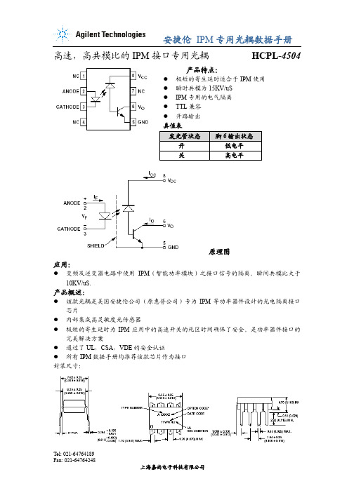
高速,高共模比的IPM 接口专用光耦 HCPL-4504产品特点:极短的寄生延时适合于IPM 使用 瞬时共模为15KV/uS IPM 专用的电气隔离 TTL 兼容 开路输出 真值表原理图应用:变频及逆变器电路中使用IPM (智能功率模块)之接口信号的隔离。
瞬间共模比大于10KV/uS.产品概述:该款光耦是美国安捷伦公司(原惠普公司)专为IPM 等功率器件设计的光电隔离接口芯片内部集成高灵敏度光传感器极短的寄生延时为IPM 应用中的高速开关的死区时间确保了安全。
是功率器件接口的完美解决方案通过了UL ,CSA ,VDE 的安全认证所有IPM 数据手册均推荐该款芯片作为接口 封装尺寸:发光管状态脚6输出状态 开 低电平 关高电平最大额定值:参数符号最小值最大值单位储存温度 TS -55 125 ℃ 工作温度 TA -55 100 ℃ 正向输入电流 IF 25 mA 输入电流峰值@1mS IF1 50 mA 输入电流峰值<1uS IF2 1 A 输入信号电压(脚3-2) VR5V输入功率 PIN 45 mA 输出电流 IO 8 mA 输出峰值电流 IOF 16 mA 控制电压(脚8-5) Vcc0.530V输出电压(脚6-5) V o 0.5 20 V 输出功率 PO 100 mW电气特性:参数符号最小值 典型值最大值单位 测试条件电流传输比 CTR 25 32 60 % IF =16mA, Vcc = 4.5V 输出低电平时 VOL 0.2 0.4 V IF =16mA, Vcc = 4.5V , IO =4mA 输出高电平时 IOH 0.01 1 μA IF=0mA, Vcc=15V , IO=4mA低电平时电源 ICCL50 200 μAIF=16mA, Vcc=15V 高电平时电源 ICCH 0.02 1 μA IF=0mA, Vcc=15V 输入正向压降 VF 1.5 1.7 V IF =16mA 输入反向电压 BVR 5VIR =10uA输入电容 Cin 60 PF F =1MHZ, VF =0V 下降沿延时 TPHL 0.2 0.3 μS F=20K,If=16mA 上升沿延时 TPLH 0.3 0.5 μS F=20K,IF=16mA 隔离耐压 VISO 2500 V 1分钟@25C隔离电阻RIO 1012Ω评估电路:1. IF :输入电流信号,假设为16mA;2. V o:输出电压信号;3. tPHL, tPLH :输入输出之间的延时;4. RL 的选择建议在10K-20K之间;5. CL的选择建议在10pF-100pF之间;6. 建议在5与8脚之间加0.1uF去偶电容;7. 7脚和8脚需要短路连接;变频设计中的死区时间和寄生延时的说明:该款产品提供了一些规格来帮助工程师“最小化死区时间”,这就是“寄生延时”误差规格。
bc547的参数全文共四篇示例,供读者参考第一篇示例:我们来看BC547的最大额定参数。
BC547的最大集电极电压一般为45伏特,最大基极电压为6伏特,而最大发射极电流一般为100毫安。
这些最大参数决定了BC547在各种电路中的安全工作范围,超过这些参数将会导致晶体管损坏。
接下来,我们来看看BC547的增益参数。
BC547的直流当前增益(hfe)一般在110到800之间,这意味着当基极电流变化时,集电极电流的变化倍数在这个范围内。
这个参数决定了BC547在放大器等电路中的放大倍数,是评价晶体管性能的重要指标之一。
除了以上两个参数外,BC547还有一些其他重要的参数。
其最大功耗一般为500毫瓦,最大工作温度一般为150摄氏度。
这些参数也是评价BC547性能和适用范围的重要指标。
第二篇示例:BC547是一种非常常用的NPN型晶体管,其参数对于电子工程师来说是非常重要的。
下面将介绍关于BC547的一些参数。
首先是极间电压,BC547的极间电压通常为50V。
这意味着在正常工作情况下,BC547可以承受最高50V的电压,这在一般的电子电路设计中是比较安全的。
BC547的最大集电极- 基极电压为45V,这意味着在正常工作情况下,集电极和基极之间的电压不应超过45V,否则可能会损坏晶体管。
BC547是一种性能稳定、使用方便的NPN型晶体管,适用于各种电子设备和电路设计中。
熟悉BC547的参数可以帮助工程师更好地选择和应用这种晶体管,确保电子设备的正常工作和性能表现。
【文章结束】。
第三篇示例:BC547是一种通用型PNP晶体管,常用于低功率放大和开关电路中。
它的参数具有很大的重要性,可以影响到整个电路的性能和稳定性。
下面我们来详细介绍一下BC547的参数。
1. 最大额定功耗(PD):BC547的最大额定功耗是500mW。
这意味着在使用BC547进行电路设计时,需要确保不超过这个功率范围,以免损坏晶体管。
2. 集电极-基极和集电极-发射极电压(VCEO、VCBO):BC547的集电极-基极和集电极-发射极电压分别为45V和50V。
SI4754C 参数手册一、概述SI4754C 是一款高性能的无线电接收器模块,广泛应用于广播接收、无线通信等领域。
该模块具有优良的信号接收能力、低功耗等特点,能够提供高质量的音频输出。
本手册将详细介绍SI4754C 的各项参数和特性,帮助您更好地理解和使用该模块。
二、物理尺寸与重量SI4754C 的物理尺寸为12mm x 12mm x 2mm,重量约为1.5 克。
三、工作电压SI4754C 的工作电压范围为2.7V 至5.5V。
建议使用3.3V 或5V 电源为模块供电。
四、工作温度范围SI4754C 的工作温度范围为-40°C 至+85°C,能够适应大多数应用场景的需求。
五、频率范围SI4754C 的频率范围覆盖了FM 和AM 广播频段,具体取决于不同的国家和地区。
具体频率范围请参考相关数据表或与供应商联系。
六、灵敏度SI4754C 的灵敏度在-106dBm 以上,能够接收微弱的信号,提高接收质量。
七、音频性能参数SI4754C 的音频输出采样率为22.05kHz 或44.1kHz,音频信噪比(SNR)大于等于80dB,失真度小于等于0.2%。
八、电源管理SI4754C 支持低功耗模式,当没有信号输入时,自动进入睡眠模式,降低功耗。
此外,SI4754C 还支持I2C 总线控制,可以通过软件进行配置和控制。
九、数字音频接口参数SI4754C 支持I2S 数字音频接口,采样率为22.05kHz 或44.1kHz,位宽为16 位或24 位。
同时,还支持左右声道独立控制和音频混合输出。
十、特殊功能说明SI4754C 支持自动搜台和手动调谐功能,可以快速找到需要的广播频道。
此外,还支持多种音频输出模式和音量控制,方便用户根据需要进行调整。
十一、引脚配置与功能描述SI4754C 模块共有24 个引脚,以下是各引脚的功能描述:1.VCC:电源正极,为模块提供工作电压。
2.GND:电源负极,接地。
日本东芝光耦深圳市美特光有限公司为日本东芝品牌光耦代理商。
TOSHIBA光耦中文名:东芝光耦。
东芝在日本东京都的总部大楼东芝(TOSHIBA),是日本最大的半导体制造商,亦是第二大综合电机制造商,隶属于三井集团旗下。
我司供应东芝全系列光耦合器,东芝光耦从功能分有逻辑输出,可控硅输出,光电二极管输出,固态继电器,高速输出,MOSFET输出,晶体管输出等。
高速光耦TLP115A描述:东芝光耦合器TLP115A是一个小外形耦合器,适合表面贴装。
TLP115A由一个高输出功率GAAℓAs发光二极管,光耦合到一个集成的高增益,高速光屏蔽检测器的输出是一个集电极开路肖特基钳位晶体管。
其中分capacirively加上常见的噪音到地面,提供1000V/μs的保证瞬变抗扰度规范。
特点:输入电流阈值:IF = 5mA (max.)切换速度:10MBD(典型值)共模瞬变抗扰度:± 1000V / μs (min.)最佳性能温度。
:0~70°C隔离电压:2500Vrms (min.)UL认证:UL1577, file no. E67349运用:高速,长距离隔离线路接收器微处理器系统接口数字隔离的A / D,D / A转换电脑外设接口接地回路消除参数:东芝高速光耦型号有:TLP550(F), TLP116A(E), 6N137F,TLP2166A(F), 6N136F,TLP2630(F),,TLP118(TPL,E),,TLP715(F),,TLP105(F), TLP108(F),,TLP557(F), 6N139(F), TLP719(TP,F), TLP2200F,6N138F,TLP559(IGM,F), TLP2309(E), TLP2631(F),TLP2098(F), TLP118(E), TLP558(F), TLP2601(F), TLP117(F), TLP718(F), TLP559(F), TLP2530(F), TLP2531(F), TLP2368(E), TLP512(F), TLP2105(F), TLP116(F), TLP2366(E), TLP115A(F), TLP716(F), TLP716(TP,F), TLP719(F), TLP714(F), TLP2118E(F), TLP2108(F),TLP2418(F), TLP2160(F), TLP2631TP1F TLP2168(F), TLP2355(E,TLP2362(E),TLP2200(TP1,F), 6N138(TP1,F), TLP2601(TP1,F), TLP2303(E TLP2303(TPR,ETLP109(IGM,E), TLP2468(F), TLP109(E), TLP2408(F), TLP104(E), TLP2409(F),TLP2358(E), TLP2301(TPL,E,TLP2303(TPL,E TLP555(F), TLP754(F), TLP2631(LF5,F), TLP2404(F), TLP2405(F), TLP2301(E,TLP2116(F), TLP2403(F), 6N137(TP1F),TLP116A(E,6N136(TP1F), TLP2630(TP1F), TLP2601(LF1,F), TLP104(TPR,E),TLP2362(TPR,E,TLP2531(TP1F), TLP2358(TPL,E), TLP2530(TP1F), TLP2116(TP,F), TLP2468(TP,F), 6N135(F), TLP559(IGM-TP5F), TLP2368(TPR,E,TLP2355(TPL,E,TLP751(F), TLP109(TPR,E), TLP2098(TPL,F), TLP2166A(TP,F), TLP118(TPR,E),TLP117(TPR,F), TLP2358(TPR,E), TLP2309(TPL,E), 6N139(TP1F), TLP109(IGM-TPR,E), TLP117(TPR,F),。