外文翻译--智能开关电源
- 格式:docx
- 大小:140.81 KB
- 文档页数:19

Switching Power Supply User Manual1.IntroductionThis switching power supply is designed for use in a wide range of electronic equipment, including computers, printers, televisions, and many other products that require a stable and efficient power supply.2.Features2.1 Efficient: The switching power supply has a high power conversion efficiency, which reduces energy waste and heat generation.2.2 Safe: The switching power supply has built-in safety features, such as over-voltage protection, over-current protection, and short-circuit protection, to ensure the safety of the equipment.2.3 Compact: The switching power supply is small and lightweight, saving space and making it easy to carry.2.4 Easy to Use: The switching power supply is easy to use and requires only a few simple steps to operate.3.Operating Instructions3.1 Connecting the Power CordConnect the power cord to the back of the switching power supply and insert it into the wall socket.3.2 Turning on the Power SupplyPress the ON/OFF button on the front panel of the switching power supply to turn it on. The power indicator will illuminate to show that the power supply is on.3.3 Adjusting the Voltage OutputUse the voltage adjustment knob on the front panel of the switching power supply to adjust the voltage output to the desired level. The user manual included with the switching power supply provides information on the correct voltage output settings for different equipment.3.4 Turning off the Power SupplyPress the ON/OFF button on the front panel of the switching power supply to turn it off. The power indicator will extinguish to show that the power supply is off.4.Safety Precautions4.1 Do not open the switching power supply or modify its internal components. This could result in electric shock or equipment failure.4.2 Ensure that the power cord is not loose or damaged and that the wall socket is in good condition. Damaged power cords should be replaced immediately.4.3 Do not insert foreign objects into the power socket or power cord to prevent electric shock or equipment failure.。
收集 B1.schematics基本翻译n. 图表网络释义schematics:图表Schematics::原理图logic schematics:逻辑框图2.Penryn网络释义Penryn:彭林|处理器|产品3.VRAM基本翻译(video RAM)视频RAM网络释义VRAM:视频随机接达记忆器|视频存储器|缓冲区VRAM-Video RAM:视频存储器VRAM VideoRAM:视频随机存取存储器4.nVIDIA基本翻译nVIDIA公司,NASDAQ:NVDA 全称为nVIDIA Corporation,创立于1993年1月,是一家以设计显示芯片和主板芯片组为主的半导体公司,总部设在美国加利福尼亚州的圣克拉拉。
是一家无自有晶圆厂(Fabless)的半导体设计公司。
网络释义Nvidia:恩威迪雅|如何安装显卡驱动|NVIDIANVIDIA RAID:高效能储存解决方案NVIDIA GPUs:阴影编辑器5.HDMI基本翻译High Definition Multimedia高清晰度多媒体接口网络释义HDMI:High-Definition Multimedia InterfaceHDMI CT:容性测试DVI-HDMI:转接头|电脑6.lvdS基本翻译LVDS:Low Voltage Differencial Signal|低压差分信号7.GMCH网络释义GMCH:芯片组|Graphics and Memory Controller HubGMCH Graphics Memory Controller Hub:图形内存控制器gmch: graphics &memory controller hub:图形和内存控制中心8.SATA网络释义SATA:串行ATAa~sata:嫂子们|嫂子SATA-IO:国际组织9.HDD基本翻译n. [计] (=hard disk drive)硬盘驱动器网络释义HDD:Hard Disk Drive|硬盘|heating degree days HDD-O:硬盘启动HDDのみ:オートリニューアル录画|楽曲再生10.USBUSB:通用串行总线|硬件技术标志:有串行总线接口USBのみ:以降USB-IF:论坛11.bluetooth基本翻译蓝牙技术网络释义Bluetooth:蓝牙|蓝牙技术|蓝芽技术Bluetooth TM:蓝牙技术|支持蓝牙|无线蓝牙Via Bluetooth:由蓝牙发送12.CMOS基本翻译n. 互补型金属氧物半导体晶体管网络释义CMOS:可读写芯片|互补金属氧化物半导体CMOSサイズ:画素数RF CMOS:半导体13.camera ['k?m?r?]基本翻译n. 照相机网络释义γ-camera:伽玛照像机on camera:出镜头|镜内表演|出现在电视上PC CAMERA:电脑摄像头|摄像头|電腦相機14.audio ['?:di?u]基本翻译a. 成音频率的,声音的网络释义Audio:音频|伴音|一不小心audio-:听M-AUDIO:美奥多15.CODEC基本翻译n. 多媒体数字信号编解码器网络释义Codec:编解码器|编码器|多媒体数字信号编解码器VSS-CODEC:编解码器电源地Line Codec:解码芯片16.amp基本翻译AMP:放大器|视骨架剖面|可利用的马达压降amp.:安瓿Y AMP:亮度放大器17.DIMM网络释义DIMM:双线内存模块|双列直插式存储器模块FB-DIMM:模块|全缓冲内存SO-DIMM:Small Outline Dual In-line Memory Module18.DDRDDR-RAM:雙通道同步動態隨機存儲器|DDR SDRAM|DDR RAM19.dual ['dju(:)?l]基本翻译a. 双重的dual:二元的双的20.modem ['m?ud?m]基本翻译调制解调器网络释义Modem:调制解调器|灯解调|解调器IF Modem:中频调制解调器SS-MODEM:解调器21.confidential [k?nfi'den??l]基本翻译a. 机密的,获他人信赖的,易于信任他人的网络释义Confidential:机密|机密的|秘密的LA confidential:洛城机密|幕后嫌疑犯(洛城机密、铁面特警队)|铁面特警队confidential a.:机密的|表示信任(或亲密)的|秘密的22.voltage ['v??ltid?]基本翻译n. 电压网络释义Voltage:电压|控制电压|电位差Y-voltage:相电压|对中性线电压Y voltage:(星形联接的)相电压23.VGA基本翻译(video graphics array)视频图形阵列网络释义VGA:可变增益放大器|Video Graphics Adapter|视频图形阵列VGA-AV:数模转换器|视频转换器RF VGA:增益放大器24.SMBus网络释义SMBus:系统管理汇流排|接口|主板芯片组25.SPI基本翻译n. 业务出版物说明(现场特殊干扰)网络释义SPI:Stateful Packet Inspection|进度绩效指数C-SPI:C-System and Process InfoationSPI CLK:外接串行接口时钟26.SCL基本翻译n. 空间电荷限制三极管网络释义SCL:时钟线|皮肤传导水平|串行时钟信号27.SDA基本翻译=Soap and Detergent Association 肥皂和洗涤剂协会[美]网络释义SDA:Secure Digital Association|串行数据信号|数据总线28.CLK网络释义CLK:时钟|输入|时钟信号S-CLK:串行时钟CLK O:时钟端29.HDCP网络释义HDCP:高带宽数字内容保护DVI-HDCP:内容保护HDCPHigh-bandwidth Digital Content Protection ::宽带宽数位内容保护30.FWR网络释义FWR:Finger Writing Recognition|速度FWR Full Wave Rectifier:全波整流器31.serial ['si?ri?l]基本翻译n. 序列,串列a. 连续的,一连串的网络释义serial:串行的.连续的|系列片|串行serial T:串联Tserial no:序列号|系列号32.EEPROM基本翻译电可擦除只读存储器网络释义EEPROM:电可檫可编程存储器|电可擦可编程只读存储器|电压消除式可程序化只读存储器IC-EEPROM:存储器LWS-EEPROM:方向盘角度传感器 EEPROM33.sensor ['sens?]基本翻译n. 传感器,探测器网络释义Sensor:传感器|感应器|感测器V-SENSOR:音声起动g-sensor:感测器34.EDP基本翻译n. 放电电渗处理(电子数据处理,工程设计建议)网络释义EDP:差错数据包|电子数据处理AFM/EDP:电子数据处理和资料系统司(数据系统司)EDP audit:电子数据处理会计|电子计算机审计35.NVVDD网络释义NVVDD:核心电压36.FB基本翻译n. 反馈(消防队,扁条,水上飞机,运货单)网络释义FB:反馈|弹性支柱|Function Block37.IFPC网络释义IFPC:推进控制|联合会|保险理财规划课程38.VID网络释义VID:视频|图像检波|视频识别模式vid,vis:看见vis,vid:看39.VDD基本翻译n. (Virtual Device Driver)虚拟设备驱动器网络释义VDD:起搏器|电圧|电源Vdd-Vss:工作电压multi-Vdd:电压40.XDP基本翻译=X-ray Density Probe X-射线密度探头[探测器]网络释义XDP:附加设备端口|附加装置端口XDP X:射线密度探头41.TDI基本翻译abbr. [计] Trandport Driver Interface 传输驱动程序接口网络释义TDI:甲苯二异氰酸酯|Test Data Input|涡轮增压直接喷射(发动机) PW-TDI:像技术42.TMS基本翻译n. 传输测试器(运输监控系统)网络释义TMS:transcranial magnetic stimulationTMS JTAG:模式控制信号Lochaine TMS:洛勤公路运输管理系统43.TDO基本翻译=Technical Data Office 技术数据处网络释义TDO:Test Data Output|一家专业生产二氧化硫脲TDO Tornado:龙卷风TDO Testing Data Out:测试数据输出44.TRST网络释义TRST:测试点|测试复位TRST JTAG:测试复位信号45.TCK基本翻译n. 轨迹(追踪)网络释义TCK:矮腥黑穗病|and Technology Compatibility KitTCK JTAG:测试时钟信号B tck to Back L/C:背对背信用证46.SCLK网络释义SCLK:频率合成器时钟|频率合成时钟信号|串行数据时钟输入端SCLK Synchronous CLocK:同步时钟SCLK SimplifiedCLocK:简化的时钟47.SDATA网络释义SDATA:高电平时触发串行数据线|频率合成数据|资料线48.alert [?'l?:t]基本翻译a. 警觉的,灵敏的,留心的网络释义alert:机灵的|警惕的|敏锐的J-ALERT:全国瞬时警报システムalert n.:报警|警戒(状态), 戒备(状态)49.VSET网络释义VSET:其电压选择|参考电压选择|充电电流控制50.GND基本翻译n. 电接地网络释义Gnd:接地|地,接地|接地点GND B:蓝色分量地线GND R:红色分量地线51.speed [spi:d]基本翻译n. 速度,迅速,超速v. 加速,超速,推进网络释义SPEED:速度|身前快速运球|生死时速x Speed:红烛时空游侠SPEED 2:生死时速2|捍卫战警252.addr基本翻译n. address的缩写内存地址网络释义ADDR:地址寄存器|寄存器addr.:缩略语BD_ADDR:蓝牙设备地址53.req网络释义req:请求文件格式〖后缀|等效电阻|需求req_dex:未知.但是可以肯定是带装备的要求req_sex:装备的性别要求54.FERR网络释义FERR:铁蛋白|帧错误ferr=iron:铁FERR Ferrite:陶铁磁体55.intr网络释义intr:执行软中断|机械制造概论|静脉注射ir intr.:去,走去caer intr.:落到,轮到56.NMI基本翻译abbr. no middle initial 无中名的姓名首字母缩写网络释义NMI:非屏蔽中断|Non-Maskable InterruptNMI-T:理接口TNMI-A:间的接口|理接口A57.SMI基本翻译n. 标准量测仪器(法定英里)网络释义SMI:Structure of Management InformationSMI-S:Storage Management Initiative Specification SMI-US:中芯国际58.defer [di'f?:]基本翻译v. 延期网络释义defer to:尊重defer vt.:推迟,延期DE Defer:延期59.DRDY网络释义DRDY:数据准备就绪DRDY-A:开关电源60.init基本翻译n. 从开关网络释义Init:初始化|预置|空闲引脚INIT# O:初始化打印机init file:初始文件61.lock [l?k]基本翻译n. 锁,刹车,水闸v. 锁,上锁,拘禁[计算机] 锁定网络释义lock:锁|上锁|锁定终端K.LOCK:操作键盘锁V-LOCK:外同步|时钟脉冲|外部同期62.BPM网络释义BPM:业务流程管理|Business Process Managemente-BPM:流程管理FD-BPM:束传输法|光束传播法63.bypass ['bai,pɑ:s]基本翻译v. 绕开, 忽视n. 支路,旁道网络释义bypass:旁路|旁通管|迂回路Bypass m:旁通,支路,旁路BY bypass:旁通64.LFE网络释义LFE:低频效果|效果|低频音效long-lfe ml:保久奶LFE Low Bit-rate Coding:低码率编码65.SDATA网络释义SDATA:高电平时触发串行数据线|频率合成数据|资料线。
本科毕业设计(论文) 外文参考文献译文及原文学院信息工程学院专业信息工程年级班别学号学生姓名指导教师目录译文 (1)基于单片机的开关电源 (1)1、用途 (1)2、简介 (1)3、分类 (2)4、开关电源的分类 (3)5、技术发展动向 (4)6、原理简介 (6)7、电路原理 (7)8、DC/DC变换 (8)9、AC/DC变换 (8)原文 (10)The design Based onsingle chip switching power supply (10)1、uses (10)2、Introduction (10)3、classification (11)4、the switching power supply. (13)5、technology developments (14)6、the principle of Introduction (17)7、the circuit schematic (18)8、the DC / DC conversion (19)9, AC / DC conversion (20)译文基于单片机的开关电源1、用途开关电源产品广泛应用于工业自动化控制、军工设备、科研设备、LED 照明、工控设备、通讯设备、电力设备、仪器仪表、医疗设备、半导体制冷制热、空气净化器,电子冰箱,液晶显示器,LED灯具,通讯设备,视听产品,安防,电脑机箱,数码产品和仪器类等领域。
2、简介随着电力电子技术的高速发展,电力电子设备与人们的工作、生活的关系日益密切,而电子设备都离不开可靠的电源,进入80年代计算机电源全面实现了开关电源化,率先完成计算机的电源换代,进入90年代开关电源相继进入各种电子、电器设备领域,程控交换机、通讯、电子检测设备电源、控制设备电源等都已广泛地使用了开关电源,更促进了开关电源技术的迅速发展。
开关电源是利用现代电力电子技术,控制开关晶体管开通和关断的时间比率,维持稳定输出电压的一种电源,开关电源一般由脉冲宽度调制(PWM)控制IC和开关器件(MOSFET、BJT等)构成。
中文4060字外文文献Switched-mode power supplyA switched-mode power supply (also switching-mode power supply, SMPS, or simply switcher) is an electronic power supply unit (PSU) that incorporates a switching regulator. While a linear regulator maintains the desired output voltage by dissipating excess power in a pass power transistor, the switched-mode power supply switches a power transistor between saturation (full on) and cutoff (completely off) with a variable duty cycle whose average is the desired output voltage. It switches at a much-higher frequency (tens to hundreds of kHz) than that of the AC line (mains), which means that the transformer that it feeds can be much smaller than one connected directly to the line/mains. Switching creates a rectangular waveform that typically goes to the primary of the transformer; typically several secondaries feed rectifiers, series inductors, and filter capacitors to provide various DC outputs with low ripple.The main advantage of this method is greater efficiency because the switching transistor dissipates little power in the saturated state and the off state compared to the semiconducting state (active region). Other advantages include smaller size and lighter weight (from the elimination of low frequency transformers which have a high weight) and lower heat generation due to higher efficiency. Disadvantages include greater complexity, the generation of high amplitude, high frequency energy that the low-pass filter must block to avoid electromagnetic interference (EMI), and a ripple voltage at the switching frequency and the harmonic frequencies thereof.A note about terminologyAlthough the term "power supply" has been in use since radios were first powered from the line/mains, that does not mean that it is a source of power, in the sense that a battery provides power. It is simply a device that (usually) accepts commercial AC power and provides one or more DC outputs. It would be more correctly referred to as a power converter, but long usage has established the term. ClassificationSMPS can be classified into four types according to the input and output waveforms: AC in, DC out: rectifier, off-line converter input stageDC in, DC out: voltage converter, or current converter, or DC to DC converterAC in, AC out: frequency changer, cycloconverter, transformerDC in, AC out: inverterInput rectifier stageIf the SMPS has an AC input, then the first stage is to convert the input to DC. This is called rectification. The rectifier circuit can be configured as a voltage doubler by the addition of a switch operated either manually or automatically. This is a feature of larger supplies to permit operation from nominally 120 volt or 240 volt supplies. The rectifier produces an unregulated DC voltage which is then sent to a large filter capacitor. The current drawn from the mains supply by this rectifier circuit occurs in short pulses around the AC voltage peaks. These pulses have significant high frequency energy which reduces the power factor. Special control techniques can be employed by the following SMPS to force the average input current to follow the sinusoidal shape of the AC input voltage thus the designer should try correcting the power factor. An SMPS with a DC input does not require this stage. An SMPS designed for AC input can often be run from a DC supply (for 230V AC this would be 330V DC), as the DC passes through the rectifier stage unchanged. It's however advisable to consult the manual before trying this, though most supplies are quite capable of such operation even though nothing is mentioned in the documentation. However, this type of use may be harmful to the rectifier stage as it will only utilize half of diodes in the rectifier for the full load. This may result in overheating of these components, and cause them to fail prematurely.If an input range switch is used, the rectifier stage is usually configured to operate as a voltage doubler when operating on the low voltage (~120 V AC) range and as a straight rectifier when operating on the high voltage (~240 V AC) range. If an input range switch is not used, then a full-wave rectifier is usually used and the downstream inverter stage is simply designed to be flexible enough to accept the wide range of dc voltages that will be produced by the rectifier stage. In higher-power SMPSs, some form of automatic range switching may be used.Inverter stageThe inverter stage converts DC, whether directly from the input or from the rectifier stage described above, to AC by running it through a power oscillator, whoseoutput transformer is very small with few windings at a frequency of tens or hundreds of kilohertz (kHz). The frequency is usually chosen to be above 20 kHz, to make it inaudible to humans. The output voltage is optically coupled to the input and thus very tightly controlled. The switching is implemented as a multistage (to achieve high gain) MOSFET amplifier. MOSFETs are a type of transistor with a low on-resistance and a high current-handling capacity. Since only the last stage has a large duty cycle, previous stages can be implemented by bipolar transistors leading to roughly the same efficiency. The second last stage needs to be of a complementary design, where one transistor charges the last MOSFET and another one discharges the MOSFET. A design using a resistor would run idle most of the time and reduce efficiency. All earlier stages do not weight into efficiency because power decreases by a factor of 10 for every stage (going backwards) and thus the earlier stages are responsible for at most 1% of the efficiency. This section refers to the block marked Chopper in the block diagram.V oltage converter and output rectifierIf the output is required to be isolated from the input, as is usually the case in mains power supplies, the inverted AC is used to drive the primary winding of a high-frequency transformer. This converts the voltage up or down to the required output level on its secondary winding. The output transformer in the block diagram serves this purpose.If a DC output is required, the AC output from the transformer is rectified. For output voltages above ten volts or so, ordinary silicon diodes are commonly used. For lower voltages, Schottky diodes are commonly used as the rectifier elements; they have the advantages of faster recovery times than silicon diodes (allowing low-loss operation at higher frequencies) and a lower voltage drop when conducting. For even lower output voltages, MOSFETs may be used as synchronous rectifiers; compared to Schottky diodes, these have even lower conducting state voltage drops.The rectified output is then smoothed by a filter consisting of inductors and capacitors. For higher switching frequencies, components with lower capacitance and inductance are needed.Simpler, non-isolated power supplies contain an inductor instead of a transformer. This type includes boost converters, buck converters, and the so called buck-boost converters. These belong to the simplest class of single input, single output converters which utilize one inductor and one active switch. The buck converter reduces the input voltage in direct proportion to the ratio of conductive time to the total switchingperiod, called the duty cycle. For example an ideal buck converter with a 10 V input operating at a 50% duty cycle will produce an average output voltage of 5 V. A feedback control loop is employed to regulate the output voltage by varying the duty cycle to compensate for variations in input voltage. The output voltage of a boost converter is always greater than the input voltage and the buck-boost output voltage is inverted but can be greater than, equal to, or less than the magnitude of its input voltage. There are many variations and extensions to this class of converters but these three form the basis of almost all isolated and non-isolated DC to DC converters. By adding a second inductor the Ćuk and SEPIC converters can be implemented, or, by adding additional active switches, various bridge converters can be realised.Other types of SMPSs use a capacitor-diode voltage multiplier instead of inductors and transformers. These are mostly used for generating high voltages at low currents (Cockcroft-Walton generator). The low voltage variant is called charge pump. RegulationA feedback circuit monitors the output voltage and compares it with a reference voltage, which is set manually or electronically to the desired output. If there is an error in the output voltage, the feedback circuit compensates by adjusting the timing with which the MOSFETs are switched on and off. This part of the power supply is called the switching regulator. The Chopper controller shown in the block diagram serves this purpose. Depending on design/safety requirements, the controller may or may not contain an isolation mechanism (such as opto-couplers) to isolate it from the DC output. Switching supplies in computers, TVs and VCRs have these opto-couplers to tightly control the output voltage.Open-loop regulators do not have a feedback circuit. Instead, they rely on feeding a constant voltage to the input of the transformer or inductor, and assume that the output will be correct. Regulated designs compensate for the parasitic capacitance of the transformer or coil. Monopolar designs also compensate for the magnetic hysteresis of the core.The feedback circuit needs power to run before it can generate power, so an additional non-switching power-supply for stand-by is added.Transformer designSMPS transformers run at high frequency. Most of the cost savings (and space savings) in off-line power supplies come from the fact that a high frequency transformer is much smaller than the 50/60 Hz transformers formerly used.There are several differences in the design of transformers for 50 Hz vs 500 kHz. Firstly a low frequency transformer usually transfers energy through its core (soft iron), while the (usually ferrite) core of a high frequency transformer limits leakage. Since the waveforms in a SMPS are generally high speed (PWM square waves), the wiring must be capable of supporting high harmonics of the base frequency due to the skin effect, which is a major source of power loss.Power factorSimple off-line switched mode power supplies incorporate a simple full wave rectifier connected to a large energy storing capacitor. Such SMPSs draw current from the AC line in short pulses when the mains instantaneous voltage exceeds the voltage across this capacitor. During the remaining portion of the AC cycle the capacitor provides energy to the power supply.As a result, the input current of such basic switched mode power supplies has high harmonic content and relatively low power factor. This creates extra load on utility lines, increases heating of the utility transformers and standard AC electric motors, and may cause stability problems in some applications such as in emergency generator systems or aircraft generators. Harmonics can be removed through the use of filter banks but the filtering is expensive, and the power utility may require a business with a very low power factor to purchase and install the filtering onsite.In 2001 the European Union put into effect the standard IEC/EN61000-3-2 to set limits on the harmonics of the AC input current up to the 40th harmonic for equipment above 75 W. The standard defines four classes of equipment depending on its type and current waveform. The most rigorous limits (class D) are established for personal computers, computer monitors, and TV receivers. In order to comply with these requirements modern switched-mode power supplies normally include an additional power factor correction (PFC) stage.Putting a current regulated boost chopper stage after the off-line rectifier (to charge the storage capacitor) can help correct the power factor, but increases the complexity (and cost).Quasiresonant ZCS/ZVSA quasiresonant ZCS/ZVS switch (Zero Current/Zero Voltage) is a design where "each switch cycle delivers a quantized 'packet' of energy to the converter output, and switch turn-on and turn-off occurs at zero current and voltage, resulting in an essentially lossless switch."EfficiencyHigher input voltage and synchronous rectification mode makes the conversion process more efficient. Higher switch frequency allows component size to be shrunk, but suffer from radio frequency (RF) properties on the other hand. The power consumption of the controller also has to be taken into account.ApplicationsSwitched-mode PSUs in domestic products such as personal computers often have universal inputs, meaning that they can accept power from most mains supplies throughout the world, with rated frequencies from 50 Hz to 60 Hz and voltages from 100 V to 240 V (although a manual voltage range switch may be required). In practice they will operate from a much wider frequency range and often from a DC supply as well. In 2006, at an Intel Developers Forum, Google engineers proposed the use of a single 12 V supply inside PCs, due to the high efficiency of switch mode supplies directly on the PCB.Most modern desktop and laptop computers already have a DC-DC converter on the motherboard, to step down the voltage from the PSU or the battery to the CPU core voltage, as low as 0.8 V for a low voltage CPU to 1.2-1.5 V for a desktop CPU as of 2007. Most laptop computers also have a DC-AC inverter to step up the voltage from the battery to drive the backlight, typically around 1000 Vrms.Certain applications, such as in automobile industry where ordinary cars often use 12 V DC and in some industrial settings, DC supply is chosen to avoid hum and interference and ease the integration of capacitors and batteries used to buffer the voltage. Most small aircraft use 28 V DC, but larger aircraft like Boeing-747 often use up to 90 kV A 3-phase at 200 V AC 400 Hz, though they often have a DC bus as well. Even fighter planes like F-16 use 400 Hz power. The MD-81 airplane has an 115/200 V 400 Hz AC and 28 V DC power system generated by three 40 kV A AC generators. Helicopters also use the 28 V DC system. Some submarines like the Soviet Alfa class submarine utilized two synchronous generators providing a variable three-phase current, 2 x 1500 kW, 400 V, 400 Hz. The space shuttle uses three fuel cells generating 30 - 36 V DC. Some is converted into 400 Hz AC power and 28 V DC power. The International Space Station uses 120 V DC power. Larger trucks uses 24 V DC.See also: Avionics, Airplane ground supportIn the case of TV sets, for example, one can test the excellent regulation of thepower supply by using a variac. For example, in some models made by Philips, the power supply starts when the voltage reaches around 90 volts. From there, one can change the voltage with the variac, and go as low as 40 volts and as high as 260 (known such case that voltage was 360), and the image will show absolutely no alterations.TerminologyThe term switchmode was widely used until Motorola trademarked SWITCHMODE(TM), for products aimed at the switching-mode power supply market, and started to enforce their trademark.外文翻译开关模式电源开关模式电源(也开关式电源,开关电源,或只是交换机)是一种电子电源供应器(电源),包含了开关稳压器。
The Introduction OfHigh Frequency Switching Power SupplyIntroduction:High frequency switching power supply (also called switch rectifier SMR) through the MOSFET or the high frequency IGBT, switch frequency control in 50-100 KHZ, within the scope of efficient and realize miniaturization. In recent years, switch rectifier power capacity expansion, the capacity of himself, from the volt 48V/12.5A、48V/20A to48V/200A、48V/400A。
High frequency switching power supply is traditional rectifier (silicon rectifier, silicon-controlled rectifier) upgrade alternative products. High frequency switching power supply with convenient use, small size, high efficiency, stable work, coating meticulous etc absolute superiority quickly dominate the market. Widely used in electroplating electrolysis surface treatment industry oxidation and get old and new customers.Product features:一.This product USES imported brand components and international advanced bridge in precision machining technology of inverter, and make the performance is stable, the quality is reliable.二.For high-frequency pulse waveforms output ripple coefficient, the 1%, can improve the number of plating and surface aestivation, refuse the gloss and got a dark corner of plating. And can reduce the loss, raw materials of plating industry of special requirements.三.SFG series high frequency switching power supply by air-filled type design, installation convenience. With remote control device, easy for operation. Can bring load switch machine, reduce the adjustment of the complex procedures.四. Small volume light weight the comprehensive use of anticorrosive craft,enhance the ability of anti-corrosion products, prolong the life.五. Energy saving, high working efficiency reached more than 90%, any more than a linear always voltage matching. Save the traditional rectifier regulator and the energy loss, in more than 35%, greatly reduce the cost, the reason of surface treatment industryHigh frequency switching power supply一.The main circuitFrom the input and output of dc exchange network, including:1.The whole the effect is input filter: there will be the clutter power filter, also hindered the feedback to produce clutter of public power.2.And rectification and filtering: ac power grid directly to a smooth dc rectification, in order to the next level.3.Inverter: after rectifying dc into high frequency alternating, this is the core part of switch power supply, the higher the frequency volume, and weight and output power than smaller.4.And output rectifier and filtering: according to provide reliable, load of the dc power supply.Second control circuit:On one hand, the sample from the output terminal with setting standards, and then compared to control the inverter, change the frequency or pulse width, achieve output stability, on the other hand, according to the test circuit, the information provided by differential protection circuit, control circuit of various protection measures.Third detection circuit:In addition to providing protection circuit is running in the various parameters but also provide various display meter data.Four, the auxiliary powerTo provide all the different requirements of a circuit switching voltage control principleSwitch to certain time interval K repeatedly through and disconnect the switch, the power input, K E through switch and filter circuits provide load RL, throughout theswitch power load during to provide energy, E, When the switch, input power disconnection K E will provide energy interrupted. Visible, to provide the energy input power load is intermittent, for the load can be provided for energy switching power supply, a storage device, must be in switch will be part of the energy stored in the switch to load, release. In the figure, the inductance and capacitance C2 and diode L circuit, is composed of D this function. Inductance used in storing energy, l., and stored in the switch of energy through the diode inductance L D, released to load get steady and continuous energy, because diode D make continuous load current, so called free-wheeling diode. In EAB average voltage between AB says: under the type used:EAB = TON/T * EFor every TON of time, the switch to switch the huge T works cycle (i.e. switch time TON TOFF cut-off time and sum).By type, changing switch time and work cycle, the ratio between the average voltage AB also changed, therefore, with the load and the input voltage changes automatically adjusted TON and the proportion of T he can make the output voltage V0 remain unchanged. Change through Time and work cycle TON of pulse that changing proportion of this method, SHCH as "Time Ratio Control" (from Time, abbreviation for TRC).According to the control principle TRC have three ways:A Pulse Width Modulation (Pulse Width Modulation, the abbreviation for PWM) Switch is constant, by changing the pulse width to change the way SHCH. Second, Pulse Frequency, Pulse Modulation (some Modulation abbreviated PFM) The constant change of the pulse width, through the working frequency switches to change the way SHCH.Third, mix modulationConduction pulse width and switch jobs are not fixed frequency, each other can change the way, and it is more than two ways of mixed.High frequency switching power supply [1] don't need to increase speed switches cantheoretically the switch loss to zero, and noise is smallThe development of switch powerSwitching power supply for has the advantages of small size, light weight, high efficiency, low calorific value and stable performance advantages and gradually replace traditional manufacturing technology of continuous work power, and widely used in electronic machine and equipment. In the 1980s, the full realization of computer, the switching power supply complete computer. In the 1990s, switch power supply in electronics, electrical equipment, and home appliance field has been widely applied; switch power technology into rapid development.Switching voltage stabilizer adopts power semiconductor as switch, through the control switch SHCH adjustment output voltage. In power transistors (GTR), for example, when a switch tube saturated conductivity, the collector and emitter on both ends of the pressure drop to zero, When the switch tube, the collector current deadline to zero. So the consumption, efficiency can be up to 70-95. While consumption also decrease. Radiator switching voltage stabilizer for grid voltage directly rectifier, filter, and then adjusted by adjusting voltage switch pipe, need not power transformer. In addition, switch frequency for dozens of KHZ, filter capacitor, inductor value. Therefore switching power supply is light weight, small size, etc.In addition, due to the low consumption, low temperature; improve the stability and reliability of the machine. And on the grid adaptive capability has increased, the average power serial Manos tat allows for 220 ± 10% fluctuate, but switching voltage stabilizer in voltage in a 110-260 volts range change, can obtain stable output voltage.The high frequency switching power supply is the development of technology innovation technology, high frequency of the benefit is that switching power supply device to miniaturization, and make an unprecedented power switch into a wide range of areas, especially in the high-tech fields of application, promote the high-tech products of miniaturization, light. Now on the market of switch power supply power tube with a bipolar transistor, switch frequency can reach several KHZ, The switch power MOSFET using frequency conversion of hundreds of KHZ. To improve theswitch frequency, must adopt high speed switching devices. For the power switch frequency than MHZ available resonant circuit this way of working is called resonant switching mode.It can greatly improve switch speed, theoretically switch loss to zero, the noise is small, and it is to improve the working frequency of switch power. By way of resonant switching converter has practical level MHZ. Pursuit of switch power supply technical development trend and can be summarized in the following four aspects.A miniaturization, thin, light, high frequency switching power supply of -- of volume, weight is mainly composed of storage devices (magnetic components and capacitance), so the miniaturization of switch power supply is essentially to minimize the volume of storage devices, In a certain range, the switch frequency, not only can effectively reduce capacitance and inductance and the size of the transformer, but also can restrain the interference, improve the dynamic performance of the system. Therefore, high frequency switching power is the main development direction.Second, high reliability - the use of switch power supply for a job than components ten times, thus increasing the reliability. From the Angle of life, capacitors, optical coupler and platoon devices such as life determines the communication power of life. So, from design, use less as far as possible, improve integration. Such not only solved the reliability of complex, the circuit, also increases protection function, simplify the circuit improve MTBF.Third, low noise - one of switch power supply noise is. Simply pursuit of high frequency and noise also is met subsequently increased. The partial resonant converting circuit technology, in principle on which can not only improve the frequency and can reduce the noise. So, as far as possible to reduce the noise influence of switch power supply is a development direction.Four, using computer aided design and control -- USES the latest technology design CDD CAA and transformation of topology and the best parameters, make the switch power structure and the best condition. Jane, in the circuit into microcomputers detection and control, monitoring system, can form multi-function real-time detection, record and automatic alarm and etc.The development of switch power supply is and semiconductor devices and the development of magnetic components. The high frequency, need corresponding high-speed semiconductorA high-frequency electromagnetic with excellent performance. Development power MOSFET, IGBT etc, develop new high-speed device with low frequency magnetic materials, improving the loss of magnetic components of the structure and the design method, enhances the filter capacitor dielectric constant and reduce its equivalent series resistor etc, to switch power miniaturization has produced a great impetus高频开关电源介绍简介高频开关电源(也称为开关型整流器SMR)通过MOSFET或IGBT的高频工作,开关频率一般控制在50-100kHz范围内,实现高效率和小型化。
Intelligent switch power supply英文:With the rapid development of electronic technology, application field of electronic system is more and more extensive, electronic equipment, there are more and more people work with electronic equipment, life is increasingly close relationship. Any electronic equipment are inseparable from reliable power supply for power requirements, they more and more is also high. Electronic equipment miniaturized and low cost in the power of light and thin, small and efficient for development direction. The traditional transistors series adjustment manostat is continuous control linear manostat. This traditional manostat technology more mature, and there has been a large number of integrated linear manostat module, has the stable performance is good, output ripple voltage small, reliable operation, etc. But usually need are bulky and heavy industrial frequency transformer and bulk and weight are big filter.In the 1950s, NASA to miniaturization, light weight as the goal, for a rocket carrying the switch power development. In almost half a century of development process, switch power because of its small volume, light weight, high efficiency, wide range, voltage advantages in electric, control, computer, and many other areas of electronic equipment has been widely used. In the 1980s, a computer is made up of all of switch power supply, the first complete computer power generation. Throughout the 1990s, switching power supply in electronics, electrical equipment, home appliances areas to be widely, switch power technology into the rapid development. In addition, large scale integrated circuit technology, and the rapid development of switch power supply with a qualitative leap, raised high frequency power products of, miniaturization, modular tide.Power switch tube, PWM controller and high-frequency transformer is an indispensable part of the switch power supply. The traditional switch power supply is normally made by using high frequency power switch tube division and the pins, such as using PWM integrated controller UC3842 + MOSFET is domestic small powerswitch power supply, the design method of a more popularity.Since the 1970s, emerged in many function complete integrated control circuit, switch power supply circuit increasingly simplified, working frequency enhances unceasingly, improving efficiency, and for power miniaturization provides the broad prospect. Three end off-line pulse width modulation monolithic integrated circuit TOP (Three switch Line) will Terminal Off with power switch MOSFET PWM controller one package together, has become the mainstream of switch power IC development. Adopt TOP switch IC design switch power, can make the circuit simplified, volume further narrowing, cost also is decreased obviouslyMonolithic switching power supply has the monolithic integrated, the minimalist peripheral circuit, best performance index, no work frequency transformer can constitute a significant advantage switching power supply, etc. American PI (with) company in Power in the mid 1990s first launched the new high frequency switching Power supply chip, known as the "top switch Power", with low cost, simple circuit, higher efficiency. The first generation of products launched in 1994 represented TOP100/200 series, the second generation product is the TOP Switch - debuted in 1997 Ⅱ. The above products once appeared showed strong vitality and he greatly simplifies thedesign of 150W following switching power supply and the development of new products for the new job, also, high efficiency and low cost switch power supply promotion and popularization created good condition, which can be widely used in instrumentation, notebook computers, mobile phones, TV, VCD and DVD, perturbation VCR, mobile phone battery chargers, power amplifier and other fields, and form various miniaturization, density, on price can compete with the linear manostat AC/DC power transformation module.Switching power supply to integrated direction of future development will be the main trend, power density will more and more big, to process requirements will increasingly high. In semiconductor devices and magnetic materials, no new breakthrough technology progress before major might find it hard to achieve, technology innovation will focus on how to improve the efficiency and focus onreducing weight. Therefore, craft level will be in the position of power supply manufacturing higher in. In addition, the application of digital control IC is the future direction of the development of a switch power. This trust in DSP for speed and anti-interference technology unceasing enhancement. As for advanced control method, now the individual feels haven't seen practicability of the method appears particularly strong,perhaps with the popularity of digital control, and there are some new control theory into switching power supply.(1)The technology: with high frequency switching frequencies increase, switch converter volume also decrease, power density has also been boosted, dynamic response improved. Small power DC - DC converter switch frequency will rise to MHz. But as the switch frequency unceasing enhancement, switch components and passive components loss increases, high-frequency parasitic parameters and high-frequency EMI and so on the new issues will also be caused.(2)Soft switching technologies: in order to improve the efficiency of non-linearity of various soft switch, commutation technical application and hygiene, representative of soft switch technology is passive and active soft switch technology, mainly including zero voltage switch/zero current switch (ZVS/ZCS) resonance, quasi resonant, zero voltage/zero current pulse width modulation technology (ZVS/ZCS - PWM) and zero voltage transition/zero current transition pulse width modulation (PWM) ZVT/ZCT - technical, etc. By means of soft switch technology can effectively reduce switch loss and switch stress, help converter transformation efficiency (3)Power factor correction technology (IC simplifies PFC). At present mainly divided into IC simplifies PFC technology passive and active IC simplifies PFC technology using IC simplifies PFC technology two kinds big, IC simplifies PFC technology can improve AC - DC change device input power factor, reduce the harmonic pollution of power grid.(4)Modular technology. Modular technology can meet the needs of the distributed power system, enhance the system reliability.(5)Low output voltage technology. With the continuous development of semiconductor manufacturing technology, microprocessor and portable electronic devices work more and more low, this requires future DC - DC converter can provide low output voltage to adapt microprocessor and power supply requirement of portable electronic devicesPeople in switching power supply technical fields are edge developing related power electronics device, the side of frequency conversion technology, development of switch between mutual promotion push switch power supply with more than two year growth toward light, digital small, thin, low noise and high reliability, anti-interference direction. Switching powersupply can be divided into the AC/DC and DC/DC two kinds big, also have AC/AC DC/AC as inverter DC/DC converter is now realize modular, and design technology and production process at home and abroad, are mature and standardization, and has approved by users, but the AC/DC modular, because of its own characteristics in the process of making modular, meet more complex technology and craft manufacture problems. The following two types of switch power supply respectively on the structure and properties of this.Switching power supply is the development direction of high frequency, high reliability, low consumption, low noise, anti-jamming and modular. Because light switch power, small, thin key techniques are changed, so high overseas each big switch power supply manufacturer are devoted to the development of new high intelligent synchronous rectifier, especially the improvement of secondary devices of the device, and power loss of Zn ferrite (Mn) material? By increasing scientific and technological innovation, to enhance in high frequency and larger magnetic flux density (Bs) can get high magnetic under the miniaturization of, and capacitor is a key technology. SMT technology application makes switching power supply has made considerable progress, both sides in the circuitboard to ensure that decorate components of switch power supply light, small, thin. The high frequency switching power supply of the traditional PWM must innovate switch technology, to realize the ZCS ZVS, soft switch technology hasbecome the mainstream of switch power supply technical, and greatly improve the efficiency of switch power. For high reliability index, America's switch power producers, reduce by lowering operating current measures such as junction temperature of the device, in order to reduce stress the reliability of products made greatly increased.Modularity is of the general development of switch power supply trend can be modular power component distributed power system, can be designed to N + 1 redundant system, and realize the capacity expansion parallel. According to switch power running large noise this one defect, if separate the pursuit of high frequency noise will increase its with the partial resonance, and transform circuit technology, high frequency can be realized in theory and can reduce the noise, but part of the practical application of resonant conversion technology still have a technical problem, so in this area still need to carry out a lot of work, in order to make the technology to practional utilization.Power electronic technology unceasing innovation, switch power supply industry has broad prospects for development. To speed up the development of switch power industry in China, we must walk speed of technological innovation road, combination with Chinese characteristics in the joint development path, for I the high-speed development of national economy to make the contribution. The basic principle and component functionAccording to the control principle of switch power to classification, we have the following 3 kinds of work mode:1) pulse width adjustment type, abbreviation Modulation Pulse Width pulse width Modulation (PWM) type, abbreviation for. Its main characteristic is fixed switching frequency, pulse width to adjust by changing voltage 390v, realize the purpose. Its core is the pulse width modulator. Switch cycle for designing filter circuit fixed provided convenience. However, its shortcomings is influenced by the power switch conduction time limit minimum of output voltage cannot be wide range regulation; In addition, the output will take dummy loads commonly (also called pre load), in order to prevent the drag elevated when output voltage. At present, most ofthe integrated switch power adopt PWM way.2) pulse frequency Modulation mode pulse frequency Modulation (, referred to Pulse Frequency Modulation, abbreviation for PFM) type. Its characteristic is will pulse width fixed by changing switch frequency to adjust voltage 390v, realize the purpose. Its core is the pulse frequency modulator. Circuit design to use fixed pulse-width generator to replace the pulse width omdulatros and use sawtooth wave generator voltage?Frequency converter (for example VCO changes frequency VCO). It on voltage stability principle is: when the output voltage Uo rises, the output signal controller pulse width unchanged and cycle longer, make Uo 390v decreases, and reduction. PFM type of switch power supply output voltage range is very wide, output terminal don't meet dummy loads. PWM way and way of PFM respectively modulating waveform is shown in figure 1 (a), (b) shows, tp says pulse width (namely power switch tube conduction time tON), T represent cycle. It can be easy to see the difference between the two. But they have something in common: (1) all use time ratio control (TRC) on voltage stability principle, whether change tp, finally adjustment or T is pulse 390v. Although adopted in different ways, but control goals, is all rivers run into the sea. (2) when load by light weight, or input voltage respectively, from high changed by increasing the pulse width, higher frequency method to make the output voltage remained stable.3) mix modulation mode, it is to point to the pulse width and switching frequency is not fixed, each other can change, it belongs to the way the PWM and PFM blend mode. It contains a pulsewidthomdulatros and pulse frequency modulator. Because and T all can adjust alone, so occupies emptiescompared to adjust the most wide range, suitable for making the output voltage for laboratories that use a wide range of can adjust switching power supply. Above 3 work collectively referred to as "Time Ratio Control" (as a Control, from TRC) way. As noted, pulse width omdulatros either as a independent IC use (for example UC3842 type pulse width omdulatros), can also be integrated in DC/DC converter (for example LM2576 type switching voltage regulators integrated circuit), still can integration in AC/DC converter (for exampleTOP250 type monolithic integrated circuit switching power supply. Among them, the switching voltage regulators belong to DC/DC power converter, switching power supply general for AC/DC power converter.The typical structure of switch power as figure1shows, its working principle is: the first utility into power rectifier and filtering into high voltage dc and then through the switch circuit and high-frequency switch to high frequency low pressure pulse transformer, and then after rectification and filter circuits, finally output low voltage dc power. Meanwhile in the output parts have a circuit feedback to control circuit, through the control PWM occupies emptiescompared to achieve output voltage stability.Figure 1 typical structure of switch power supplySwitching power supply by these four components:1) the main circuit: exchange network input, from the main circuit to dc output. Mainly includes input filter, rectifier and filtering, inverter, and output rectifier and filtering.(1) input filter: its effect is the power grid existing clutter filtering, also hinder the machine produces clutter feedback to public power grid.(2) rectifier and filter: the power grid ac power directly for a smooth dc rectifier, for the next level transformation.(3) inverter: will the dc after rectifying a high-frequency ac, this is the core of high frequency switching power supply, the higher the frequency, the volume, weight and the ratio of power output and smaller.(4) Out put rectifier and filter: according to load needs, providing stable and reliable dc power supply. 2) control circuit: on the one hand, from the output bysampling with set standards to compare, and then to control inverter, changing its frequency or pulse width, achieve output stability, on the other hand, according to data provided by the test circuit, the protection circuit differential, provide control circuit to the machine to various protection measures. Including the output feedback circuit and sampling circuit, pulse width modulator. 3) the detection and protection circuit: detection circuit had current detection, over-voltage detection, owe voltage detection, overheat detection, etc.; Protection circuit can be divided over current protection, over-voltage protection, owe voltage protection, the ground-clamp protection, overheating protection, automatic restart, soft start, slow startup, etc. Various types. 4) Other circuit: if the sawtooth wave generator, offset circuit, optical coupler, etc.智能开关电源中文:随着电子技术的高速发展,电子系统的应用领域越来越广泛,电子设备的种类也越来越多,电子设备与人们的工作、生活的关系日益密切。
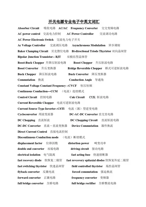
开关电源专业电子中英文词汇Absorber Circuit 吸收电路AC/AC Frequency Converter 交交变频电路AC power control交流电力控制AC Power Controller交流调功电路AC Power Electronic Switch交流电力电子开关Ac Voltage Controller交流调压电路Asynchronous Modulation异步调制Baker Clamping Circuit 贝克箝位电路Bi-directional Triode Thyristor双向晶闸管Bipolar Junction Transistor-- BJT双极结型晶体管Boost-Buck Chopper 升降压斩波电路Boost Chopper 升压斩波电路Boost Converter 升压变换器Bridge Reversible Chopper 桥式可逆斩波电路Buck Chopper 降压斩波电路Buck Converter 降压变换器Commutation 换流Conduction Angle 导通角Constant Voltage Constant Frequency --CVCF 恒压恒频Continuous Conduction—CCM (电流)连续模式Control Circuit 控制电路Cuk Circuit CUK 斩波电路Current Reversible Chopper 电流可逆斩波电路Current Source Type Inverter--CSTI 电流(源)型逆变电路Cycloconvertor 周波变流器DC-AC-DC Converter直交直电路DC Chopping 直流斩波DC Chopping Circuit 直流斩波电路DC-DC Converter 直流-直流变换器Device Commutation 器件换流Direct Current Control 直接电流控制Discontinuous Conduction mode (电流)断续模式displacement factor 位移因数distortion power 畸变功率double end converter 双端电路driving circuit 驱动电路electrical isolation 电气隔离fast acting fuse 快速熔断器fast recovery diode 快恢复二极管fast revcovery epitaxial diodes快恢复外延二极管fast switching thyristor 快速晶闸管field controlled thyristor 场控晶闸管flyback converter 反激电流forced commutation 强迫换流forward converter 正激电路frequency converter 变频器full bridge converter 全桥电路full bridge rectifier 全桥整流电路full wave rectifier 全波整流电路fundamental factor 基波因数gate turn-off thyristor——GTO可关断晶闸管general purpose diode普通二极管giant transistor——GTR电力晶体管half bridge converter 半桥电路hard switching 硬开关high voltage IC 高压集成电路hysteresis comparison 带环比较方式indirect current control 间接电流控制indirect DC-DC converter 直接电流变换电路insulated-gate bipolar transistor-----IGBT绝缘栅双极晶体管intelligent power module-------IPM智能功率模块integrated gate-commutated thyristor------IGCT集成门极换流晶闸管inversion 逆变latching effect 擎住效应leakage inductance 漏感light triggered thyristo---LTT光控晶闸管line commutation 电网换流load commutation 负载换流loop current 环流Schottky Barrier Diode 肖特基二极管。
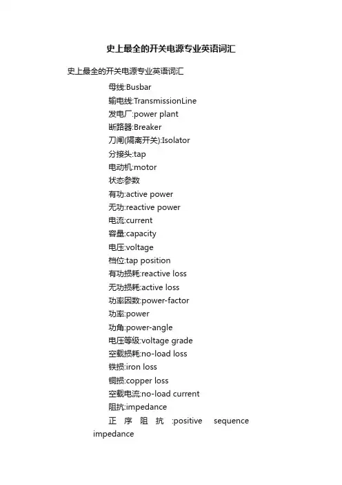
史上最全的开关电源专业英语词汇史上最全的开关电源专业英语词汇母线:Busbar输电线:TransmissionLine发电厂:power plant断路器:Breaker刀闸(隔离开关):Isolator分接头:tap电动机:motor状态参数有功:active power无功:reactive power电流:current容量:capacity电压:voltage档位:tap position有功损耗:reactive loss无功损耗:active loss功率因数:power-factor功率:power功角:power-angle电压等级:voltage grade空载损耗:no-load loss铁损:iron loss铜损:copper loss空载电流:no-load current阻抗:impedance正序阻抗:positive sequence impedance负序阻抗:negative sequence impedance零序阻抗:zero sequence impedance电阻:resistor电抗:reactance电导:conductance电纳:susceptance无功负载:reactive load 或者QLoad有功负载: active load PLoad遥测:YC(telemetering)遥信:YX励磁电流(转子电流):magnetizing current定子:stator功角:power-angle上限:upper limit下限:lower limit并列的:apposable高压: high voltage低压:low voltage中压:middle voltage电力系统 power system发电机 generator励磁 excitation励磁器 excitor电压 voltage电流 current母线 bus变压器 transformer升压变压器 step-up transformer高压侧 high side输电系统 power transmission system输电线 transmission line固定串联电容补偿fixed series capacitor compensation稳定 stability电压稳定 voltage stability功角稳定 angle stability暂态稳定 transient stability电厂 power plant能量输送 power transfer交流 AC装机容量 installed capacity电网 power system落点 drop point开关站 switch station双回同杆并架double-circuit lines on the same tower变电站 transformer substation补偿度 degree of compensation高抗 high voltage shunt reactor无功补偿reactive power compensation故障 fault调节 regulation裕度 magin三相故障 three phase fault故障切除时间 fault clearing time极限切除时间 critical clearing time切机 generator triping高顶值 high limited value强行励磁 reinforced excitation线路补偿器LDC(line drop compensation)机端 generator terminal静态 static (state)动态 dynamic (state)单机无穷大系统 one machine - infinity bus system机端电压控制 AVR电抗 reactance电阻 resistance功角 power angle有功(功率) active power无功(功率) reactive power功率因数 power factor无功电流 reactive current下降特性 droop characteristics斜率 slope额定 rating变比 ratio参考值 reference value电压互感器 PT分接头 tap下降率 droop rate仿真分析 simulation analysis传递函数 transfer function框图 block diagram受端 receive-side裕度 margin同步 synchronization失去同步 loss of synchronization 阻尼 damping摇摆 swing保护断路器 circuit breaker电阻:resistance电抗:reactance阻抗:impedance电导:conductance电纳:susceptance导纳:admittance电感:inductance电容: capacitance电源英语词汇(三)coupling 耦合intermittent 周期的dislocation 错位propeller 螺旋桨switchgear 配电装置dispersion 差量flange 法兰盘dielectric 介电的binder 胶合剂alignment 定位elastomer 合成橡胶corollary 必然的结果rabbet 插槽vent 通风孔subtle 敏感的gearbox 变速箱plate 电镀crucial 决定性的flexible 柔性的technics 工艺ultimate 最终的resilience 弹性vendor 自动售货机partition 分类rigid 刚性的prototype 样机diagram 特性曲线interfere 干涉compatible 兼容的simulation 模拟clutch 离合器refinement 精加工fixture 夹具torque 扭矩responsive 敏感的tensile 拉伸cushion 减震器rib 肋strength 强度packing 包装metallized 金属化stress 应力mitigate 减轻trade off 折衷方案yield 屈伸line shaft 中间轴matrix 母体inherent 固有的spindle 主轴aperture 孔径conformance 适应性axle 心轴turbulence 扰动specification 规范semipermanent 半永久性的enclosure 机壳specialization 规范化bolt 螺栓oscillation 振幅calling 职业nut 螺母anneal 退火vitalize 激发screw 螺丝polymer 聚合体revelation 揭示fastner 紧固件bind 凝固dissemination 分发rivit 铆钉mount 支架booster 推进器hub 轴套distortion 变形contractual 契约的coaxial 同心的module 模块verdict 裁决crank 曲柄slide 滑块malfunction 故障inertia 惰性medium 介质allegedly 假定active 活性的dissipation 损耗controversy 辩论lubrication 润滑assembly 总装dictate 支配graphite 石墨encapsulate 封装incumbent 义不容辞的derivative 派生物adhesive 粘合剂validation 使生效contaminate 沾染turbine 涡轮procurement 收购asperity 粗糙bearing 支撑架mortality 失败率metalworking 金属加工isostatic 均衡的shed light on 阐明viscous 粘稠的osculate 接触adversely 有害的grinding 研磨imperative 强制的consistency 连续性corrosin 侵蚀lattice 晶格fitness 适应性flush 冲洗fracture 断裂warrant 保证inhibitor 防腐剂diffusivity 扩散率turning 车工dispersant 分散剂vice versa 反之亦然ways 导轨deteriorate 降低tribological 摩擦的hybrid 混合物neutralize 平衡screen 屏蔽ID=inside diameterpulley 滑轮exclusion 隔绝OD=outside diameter hydraulic 液压的insulation 绝缘reciprocate 往复运动delicate 精密的elaborate 加工dress 精整dampen 阻尼incontrovertible 无可争议的by and large 大体上pivotal 中枢的luminous 发光的plastic 塑胶utilitarian 功利主义out of round 失园organic 有机的grass root 基层premature 过早的film 薄膜state-of-the -art 技术发展水平guard 防护罩polyester 聚酯blade 托板permeate 渗入epoxy 环氧的carrier 载体spillage 溢出polypropylene 聚丙烯chuck 卡盘erosion 浸蚀photoconductive 光敏的infeed 横向进给routine 程序miniaturization 小型化lapping 抛光postprocess 后置处理asynchronism 异步milling 洗削solder-bump 焊点synchronization 同步speciality 专业grid 栅格respond 响应stroke 行程impedance 阻抗feedback 反馈attachment 备件approximately 大约aberrance 畸变tapered 楔形的purported 据说steady 稳态的casting 铸件consumable 消费品dynamic 动态的index 换档inductance 电感transient 瞬态的stop 挡块capacitance 电容coordinate 坐标contour 轮廓resistance 电容curve 曲线machine center 加工中心audion 三极管diagram 特性曲线capitalize 投资diode 二极管history 关系曲线potentiometer 电位器transistor 晶体管gradient 斜率know-how 实践知识choker 扼流圈parabola 抛物线potted 封装的filter 滤波器root 根mechatronics 机电一体化transformer 变压器eigenvalue 特征值stem from 起源于fuse 保险丝function 函数rule-based 基于规则的annular core 磁环vector 向量consolidation 巩固radiator 散热器reciprocal 倒数energize 激发regulator 稳压器virtual value 有效值synchronous 同时发生bobbin 骨架square root 平方根socket 插孔tape 胶带cube 立方polarity 极性ceramic capacitor 瓷片电容integral 积分armature 电枢electrolytic C 电解电容differential 微分installment 分期付款self-tapping screw 自攻螺丝hisgram 直方图lobe 凸起footprint 封装ratio 比率plunge 钻入resin 松香grade down 成比例降低servo 伺服机构solderability 可焊性proportion 比例dedicated 专用的shock 机械冲击inverse ratio 反比interpolation 插补endurance 耐久性direct ratio 正比compensation 校正initial value 初始值plus 加upload 加载flashing 飞弧subtract 减overload 过载canned 千篇一律的multiply 乘lightload 轻载lot 抽签divide 除stagger 交错排列parallel 并联impedance 阻抗traverse 横向in series 串联damp 阻尼longitudinal 纵向的equivalent 等效的reactance 电抗latitudinal 横向的terminal 终端admittance 导纳restrain 约束creep 蠕动susceptance 电纳square 平方Hyperlink 超级连接spring 触发memo 备忘录wastage 损耗presentation 陈述principle 原理binder 打包planer 刨床source program 源程序Client-Server Model客户机server 服务器table 表query 查询form 表单report 报表macro 宏module 模块field 字段record 记录。
外文资料译文THE DEVELOPMENT OF SWITCHING POWER 1955 United States Royer (GH.Roger) invented the transistor single push-pull oscillation transformer DC-DC converter, frequency conversion control circuit to achieve the beginning of 1957, the United States Charles race (Jen Sen) invented the self-excited push-pull double transformer, in 1964 U.S. scientists have proposed to abolish the frequency transformer switching power supply series idea, which is the power to decline in volume and weight were a fundamental way. To 1969 because of pressure to improve high-power silicon transistors, diode reverse recovery time shortened components to improve, and finally made a 25 kHz switching power supply. At present, switching power supply to small, light weight and high efficiency characteristics are widely used in a variety of computer-driven devices, communications equipment, etc. Almost all the electronic equipment is the rapid development of today's electronic information industry, an indispensable Power Source. Currently on the market the use of switching power bipolar transistors made of 100kHz, 500kHz with a power MOSFET made, Although practical, its frequency needs to be improved. To improve the switching frequency, it is necessary to reduce switching losses, and to reduce switching losses, it needs high-speed switching components. However, the switching speed of the increase will be distributed by the circuit inductance and capacitance, or diode stored charge of the generated surge or noise. This will not only affect nearby electronic equipment, will greatly reduce the reliability of power supply itself. Which, with the switch to prevent Kai - closed by the voltage surge occurs, can use RC or LC buffer, while the stored charge from the diode can be used due to current surges such as core made of amorphous magnetic buffer .However, for more than 1MHz frequency, resonant circuit to be used to make the switch voltage or current through the switch was a sine wave, this can reduce the switching losses, but also to control the occurrence of surge. This switch is called resonant switch. Current switching power supply of this very active, because this approach does not require substantial increase in switching speed can be reduced theoretically to zero switching losses and noise are small, is expected to be of a high-frequency switching power supply main ways. At present, many countries are working on a few trillion Hz, the practical application of converter.Switching power supply direction of development is high-frequency, high reliability, low power, low noise, interference and modular. Oxygen material increase scientific and technological innovation to enhance the high frequency and higher magnetic flux density (Bs) obtained a high magnetic properties, while the small capacitor is a key technology. SMT technology allows switching power supply hasmade considerable progress, both sides of the circuit board layout components to ensure that the switching power supply of light, small, thin. High frequency switching power supply will be bound to the traditional PWM switching technology innovation, realization of ZVS, ZCS soft switching power supply switching technology has become the mainstream technology, and a substantial increase in the switching power supply efficiency.For high reliability, the U.S. manufacturer of switching power supply by reducing operating current to reduce junction temperature and other measures to reduce the stress of the device makes the improved reliability of products.Modular switching power supply is the general trend of development can be composed of modular power distributed power systems can be designed to N +1 redundant power systems, and parallel way to achieve the capacity expansion. Switching power supply noise for the big run this shortcoming, if the individual pursuit of its high-frequency noise will also increase with, while using some of the resonant converter circuit technology, in theory, but also can reduce the high frequency of the noise, but some the practical application of resonant conversion technology, there are still technical problems, it still required much work in this area in order to make the technology to practical use.With the power electronics technology development, switching power supply industry has a bright future. Switching power supply industry in China should speed up the pace of development, we must take the technical innovation, out of the Industry and Academia with Chinese characteristics development road, as the rapid development of our national economy to contribute.开关电源的发展1955年美国罗耶(GH.Roger)发明的自激振荡推挽晶体管单变压器直流变换器,是实现高频转换控制电路的开端,1957年美国查赛(Jen Sen)发明了自激式推挽双变压器,1964年美国科学家们提出取消工频变压器的串联开关电源的设想,这对电源向体积和重量的下降获得了一条根本的途径。

开关电源外文翻译()————————————————————————————————作者:————————————————————————————————日期:Modeling, Simulation, and Reduction of Conducted Electromagnetic Interference Due to a PWM Buck Type Switching Power Supply IA. FarhadiAbstract:Undesired generation of radiated or conducted energy in electrical systems is called Electromagnetic Interference (EMI). High speed switching frequency in power electronics converters especially in switching power supplies improves efficiency but leads to EMI. Different kind of conducted interference, EMI regulations and conducted EMI measurement are introduced in this paper. Compliancy with national or international regulation is called Electromagnetic Compatibility (EMC). Power electronic systems producers must regard EMC. Modeling and simulation is the first step of EMC evaluation. EMI simulation results due to a PWM Buck type switching power supply are presented in this paper. To improve EMC, some techniques are introduced and their effectiveness proved by simulation.Index Terms:Conducted, EMC, EMI, LISN, Switching SupplyI. INTRODUCTIONFAST semiconductors make it possible to have high speed and high frequency switching in power electronics []1. High speed switching causes weight and volume reduction of equipment, but some unwanted effects such as radio frequency interference appeared []2. Compliance with electromagnetic compatibility (EMC) regulations is necessary for producers to present their products to the markets. It is important to take EMC aspects already in design phase []3. Modeling and simulation is the most effective tool to analyze EMC consideration before developing the products. A lot of the previous studies concerned the low frequency analysis of power electronics components []4[]5. Different types of power electronics converters are capable to be considered as source of EMI. They could propagate the EMI in both radiated and conducted forms. Line Impedance Stabilization Network (LISN) is required for measurement and calculation of conducted interference level []6. Interference spectrum at the output of LISN is introduced as the EMC evaluation criterion []7[]8. National or international regulations are the references for the evaluation of equipment in point of view of EMC []7[]8.II. SOURCE, PATH AND VICTIM OF EMIUndesired voltage or current is called interference and their cause is called interferencesource. In this paper a high-speed switching power supply is the source of interference.Interference propagated by radiation in area around of an interference source or by conduction through common cabling or wiring connections. In this study conducted emission is considered only. Equipment such as computers, receivers, amplifiers, industrial controllers, etc that are exposed to interference corruption are called victims. The common connections of elements, source lines and cabling provide paths for conducted noise or interference. Electromagnetic conducted interference has two components as differential mode and common mode []9.A. Differential mode conducted interferenceThis mode is related to the noise that is imposed between different lines of a test circuit by a noise source. Related current path is shown in Fig. 1 []9. The interference source, path impedances, differential mode current and load impedance are also shown in Fig. 1.B. Common mode conducted interferenceCommon mode noise or interference could appear and impose between the lines, cables or connections and common ground. Any leakage current between load and common ground could be modeled by interference voltage source.and Fig. 2 demonstrates the common mode interference source, common mode currents Icm1 and the related current paths[]9.The power electronics converters perform as noise source Icm2between lines of the supply network. In this study differential mode of conducted interference is particularly important and discussion will be continued considering this mode only.III. ELECTROMAGNETIC COMPATIBILITY REGULATIONS Application of electrical equipment especially static power electronic converters in different equipment is increasing more and more. As mentioned before, power electronics converters are considered as an important source of electromagnetic interference and have corrupting effects on the electric networks []2. High level of pollution resulting from various disturbances reduces the quality of power in electric networks. On the other side some residential, commercial and especially medical consumers are so sensitive to power system disturbances including voltage and frequency variations. The best solution to reduce corruption and improve power quality is complying national or international EMC regulations. CISPR, IEC, FCC and VDE are among the most famous organizations from Europe, USA and Germany who are responsible for determining and publishing the most important EMC regulations. IEC and VDE requirement and limitations on conducted emission are shown in Fig. 3 and Fig. 4 []7[]9.For different groups of consumers different classes of regulations could be complied. Class A for common consumers and class B with more hard limitations for special consumers are separated in Fig. 3 and Fig. 4. Frequency range of limitation is different for IEC and VDE that are 150 kHz up to 30 MHz and 10 kHz up to 30 MHz respectively. Compliance of regulations isevaluated by comparison of measured or calculated conducted interference level in the mentioned frequency range with the stated requirements in regulations. In united European community compliance of regulation is mandatory and products must have certified label to show covering of requirements []8.IV. ELECTROMAGNETIC CONDUCTED INTERFERENCE MEASUREMENTA. Line Impedance Stabilization Network (LISN)1-Providing a low impedance path to transfer power from source to power electronics converter and load.2-Providing a low impedance path from interference source, here power electronics converter, to measurement port.Variation of LISN impedance versus frequency with the mentioned topology is presented inFig. 7. LISN has stabilized impedance in the range of conducted EMI measurement []7.Variation of level of signal at the output of LISN versus frequency is the spectrum of interference. The electromagnetic compatibility of a system can be evaluated by comparison of its interference spectrum with the standard limitations. The level of signal at the output of LISN in frequency range 10 kHz up to 30 MHz or 150 kHz up to 30 MHz is criterion of compatibility and should be under the standard limitations. In practical situations, the LISN output is connected to a spectrum analyzer and interference measurement is carried out. But for modeling and simulation purposes, the LISN output spectrum is calculated using appropriate software.For a simple fixed frequency PWM controller that is applied to a Buck DC/DC converter, it is) changes slow with respect to the switching frequency, the possible to assume the error voltage (vepulse width and hence the duty cycle can be approximated by (1). Vp is the saw tooth waveform amplitude.A. PWM waveform spectral analysisThe normalized pulse train m (t) of Fig. 8 represents PWM switch current waveform. The nth pulse of PWM waveform consists of a fixed component D/fs , in which D is the steady state duty cycle, and a variable component dn/f sthat represents the variation of duty cycle due to variation of source, reference and load.As the PWM switch current waveform contains information concerning EMI due to powersupply, it is required to do the spectrum analysis of this waveform in the frequency range of EMI studies. It is assumed that error voltage varies around V e with amplitude of V e1 as is shown in (2).fm represents the frequency of error voltage variation due to the variations of source, reference and load. The interception of the error voltage variation curve and the saw tooth waveform with switching frequency, leads to (3) for the computation of duty cycle coefficients []10.Maximum variation of pulse width around its steady state value of D is limited to D1. In each period of Tm=1/fm , there will be r=fs/fm pulses with duty cycles of dn. Equation (4) presents the Fourier series coefficients Cn of the PWM waveform m (t). Which have the frequency spectrum of Fig.9.B-Equivalent noise circuit and EMI spectral analysisTo attain the equivalent circuit of Fig.6 the voltage source Vs is replaced by short circuit and) as it has shown in Fig. 10. converter is replaced by PWM waveform switch current (IexThe transfer function is defined as the ratio of the LISN output voltage to the EMI current source as in (5).The coefficients di, ni (i = 1, 2, … , 4) correspond to the parameters of the equivalent circuit. Rc and Lc are respectively the effective series resistance (ESR) and inductance (ESL) of the filter capacitor Cf that model the non-ideality of this element. The LISN and filter parameters are as follows: CN = 100 nF, r = 5 Ω, l = 50 uH, RN =50 Ω, LN=250 uH, Lf = 0, Cf =0, Rc= 0, Lc= 0, fs =25 kHzThe EMI spectrum is derived by multiplication of the transfer function and the source noise spectrum. Simulation results are shown in Fig. 11.VI. PARAMETERS AFFECTION ON EMIA. Duty CycleThe pulse width in PWM waveform varies around a steady state D=0.5. The output noise spectrum was simulated with values of D=0.25 and 0.75 that are shown in Fig. 12 and Fig. 13. Even harmonics are increased and odd ones are decreased that is desired in point of view of EMC.On the other hand the noise energy is distributed over a wider range of frequency and the level of EMI decreased []11.B. Amplitude of duty cycle variationThe maximum pulse width variation is determined by D1. The EMI spectrum was simulatedwith D1=0.05. Simulations are repeated with D1=0.01 and 0.25 and the results are shown in Fig.14and Fig.15.Increasing of D1 leads to frequency modulation of the EMI signal and reduction in level of conducted EMI. Zooming of Fig. 15 around 7th component of switching frequency in Fig. 16 shows the frequency modulation clearly.C. Error voltage frequencyThe main factor in the variation of duty cycle is the variation of source voltage. The fm=100 Hz ripple in source voltage is the inevitable consequence of the usage of rectifiers. The simulation is repeated in the frequency of fm=5000 Hz. It is shown in Fig. 17 that at a higher frequency for fm the noise spectrum expands in frequency domain and causes smaller level of conducted EMI. On the other hand it is desired to inject a high frequency signal to the reference voltage intentionally.D. Simultaneous effect of parametersSimulation results of simultaneous application of D=0.75, D1=0.25 and fm=5000 Hz that leadto expansion of EMI spectrum over a wider frequencies and considerable reduction in EMI level is shown in Fig. 18.VII. CONCLUSIONAppearance of Electromagnetic Interference due to the fast switching semiconductor devices performance in power electronics converters is introduced in this paper. Radiated and conducted interference are two types of Electromagnetic Interference where conducted type is studied in this paper. Compatibility regulations and conducted interference measurement were explained. LISN as an important part of measuring process besides its topology, parameters and impedance were described. EMI spectrum due to a PWM Buck type DC/DC converter was considered and simulated. It is necessary to present mechanisms to reduce the level of Electromagnetic interference. It shown that EMI due to a PWM Buck type switching power supply could be reduced by controlling parameters such as duty cycle, duty cycle variation and reference voltage frequency.VIII. REFRENCES[1] Mohan, Undeland, and Robbins, “Power Electronics Converters, Applications and Design” 3rdedition, John Wiley & Sons, 2003.[2] P. Moy, “EMC Related Issues for Power Electronics”, IEEE, Automotive Pow er Electronics, 1989, 28-29 Aug. 1989 pp. 46 – 53.[3] M. J. Nave, “Prediction of Conducted Interference in Switched Mode Power Supplies”, Session 3B, IEEE International Symp. on EMC, 1986.[4] Henderson, R. D. and Rose, P. J., “Harmonics and their Effec ts on Power Quality and Transformers”, IEEE Trans. On Ind. App., 1994, pp. 528-532.[5] I. Kasikci, “A New Method for Power Factor Correction and Harmonic Elimination in Power System”, Proceedings of IEEE Ninth International Conference on Harmonics and Q uality of Power, Volume 3, pp. 810 – 815, Oct. 2000.[6] M. J. Nave, “Line Impedance Stabilization Networks: Theory and Applications”, RFI/EMI Corner, April 1985, pp. 54-56.[7] T. Williams, “EMC for Product Designers” 3rd edition 2001 Newnes.[8] B. Ke isier, “Principles of Electromagnetic Compatibility”, 3rd edition ARTECH HOUSE 1987.[9] J. C. Fluke, “Controlling Conducted Emission by Design”, Vanhostrand Reinhold 1991.[10] M. Daniel,”DC/DC Switching Regulator Analysis”, McGrawhill 1988[11] M. J. Nave,” The Effect of Duty Cycle on SMPS Common Mode Emission: theory and experiment”, IEEE National Symposium on Electromagnetic Compatibility, Page(s): 211-216, 23-25 May 1989.作者:A. Farhadi国籍:伊朗出处:基于压降型PWM开关电源的建模、仿真和减少传导性电磁干扰IIA. Farhadi作者:A. Farhadi国籍:伊朗出处:摘要:电子设备之中杂乱的辐射或者能量叫做电磁干扰(EMI)。
NC switching power supplyAbstract:This system based on 51 SCM control unit, used for LM2576-wild numerical control a switching power supply of fuzzy digital control technology, adjust load R1, R2 proportion to change occupies empties compared to make the output stability, and can be through the buttons, digital display to realize output voltage numerical control. In addition, the system to input pressure, flow, input output flow, switch tube overheat as well as the protection circuit, ensure that the system is stable and reliable.Key words:the numerical control,switching power supply,LM2576-wild,micro controller (一)The overall design of the systemSystem to monolithic integrated circuit AT89S52, LM2576-for the core part, and the wild through the monolithic integrated circuit to output voltage gather, comparison, operations, and the output voltage control, automatic regulation system structure diagram shown as shown in figure 1.220 V / 50 Hz ac voltage after rectifying circuit and DC/DC voltage chip LM2576 wild transformation for stable-5 ~ 12 V DC voltage output, the output voltage through sampling circuit by sampling, A/D conversion chip ADC0804 after converting to 52 after processing, control simulation electron switch to choose 4051 respectively the nine potentiometer R2, change R1 and R2 ratio values, which change LM2576-of the wild chip PWM pulse of empty, MOS tubes work than to switch state in, the input of 15 V DC voltage "chopped" for the and of the same frequency PWM waves pulse wave, pulse wave through the rectifier filter circuit output for 5 ~ 12 V DC voltage. Because of this the topic request have nine output stepping demand, so can tune in advance each voltage resistance, through the corresponding key choice output voltage, directly to the analog switch 4067 choose resistance, they can get to output voltage. At the same time, to detect the voltage, current value through the display LCD1062 real-time display. If working current is too big, the flow detection circuit will be sent to the testing results of single-chip microcomputer, SCM control relaythrough the ac branch realize over-current protection system in fault, after the operation is set by the reset button to may cause the system to resume normal work. (二)The block diagram of the whole system(三) Unit circuit function and the analysis of the operation1. Minimum AT89S52 SCM systemMinimum system including crystal oscillator circuit and reset switch and power supply parts. Figure 2 for the minimum AT89S52 SCM system.The wave rectifier circuit is made up of two half wave of rectifier circuit. Because in the next two, add on miens input voltage of the opposite polarity, therefore, to a dynamic balance, in every signal cycle, the C1 and C2 experience 2 times charger, discharge process, current will appear two current pulse with polarity. So in addition to the V o saw tooth wave on the wavy frequency, improve the ability of double filtering, thus reduce ripple voltage.The dc power by power supply, filtering, protection, such as voltage, four basic modules.(1)The power transformer USES a step-down transformer, the power grid voltage 220 V transform into need ac voltage. The ac voltageAfter rectifying, may obtain electronic equipment need dc voltage.(2) Use rectifier circuit bridge rectifier circuit single-phase, 50 Hz ac alternating current transformation for direction invariable but still has the pulse size straight Flow electricity. Its advantage is high voltage ripple voltage, small, the utilization rate of transformer high. This design by A bridge pile of bridge rectifier, RS808 do maximum current can reach 8 A, cooperate with the design of the large filter capacitance, so the power of the instantaneous large current power supply characteristics, low noise, good reaction speed, output ripple small.(3)Filter circuit using capacitance filter circuit, will the pulsation of the rectifier circuit output filter, get most of the components is smooth dc the electricity. This circuit adopts 4700 u F / 50 V large capacitance C3, C4 to make the output voltage more smooth, the power supply characteristics moment, suitable for take the perceptual load, such as motor start-up. C3, C4 every parallel connection a 0.1 u F / 63 V CBB capacitance, filter to high frequency interference, make input to integrated circuits L11, L12 of dc as far as possible the smooth and pure.(4)By LM317 output voltage circuit is power, LM337 output negative supply. LM317 and LM337 are used internal heat Load, contains over current protection, hot off and safety working area for perfect protection circuit, that power can save the fuse, and so easy loss device. Regulating circuit: to meet the needs of the differentapplication situation and the voltage is set to can be adjusted. The calculation of the output voltage V o = 1.25 x (1 + Rf/R), adjustable resistance in use precision can be resistor and guarantee the precise output voltage can be adjusted. If this article chooses for 5 k of Rf Ω, R for 270 Ω combination, can respectively on 1.25 V ~ 24 V 1.25 V ~ 24 V achieve continuous adjustable between.(5)Protection circuit for linear power supply heat, so the power larger add enough radiator. Due to the high performance integrated circuit, which can simplify the circuit structure, highlighting the important part in the power transformation. Through the commissioning and testing, good performance. The whole circuit The power not only can be used alone, also can be in other electronic equipment used in voltage or current stabilization source use.2. LM2576-voltage circuit wildWorking principle:Assume that the switch transistors, diodes are ideal components, inductance and capacitance is ideal components, the output voltage ripple voltage output voltage and the ratio of the small to allow oversight.According to the current cycle to begin in IL inductance is starting from scratch, can be divided into current continuous working mode and inductance inductive current is discontinuous work patterns. Due to the continuous work mode inductance current converter, have very good control characteristic; Inductive current is discontinuous work mode, put the electric, inductance and capacitance easy to produce the oscillation, thus affecting the output voltage ripple; And the same occupies empties compared, output voltage in discrete model under the mode of work than the big, high efficiency. To sum up, the most ideal situation is in critical condition, stabilizer which work so we use two kinds of methods:(1)The increase of the inductance inductive energy storage, increase, and extend the discharge of time(2)Improve the work and reduce the frequency switch timeMake transistor in current continuous state.3. The whole wave output rectifier circuit parameter analysisOutput filter by free-wheeling diode rectifier circuit, inductance and capacitance composition. Consider free-wheeling diode in tube by PMOS transistor conduction, when energy consumption, and work in the state, so we used the low power consumption, high current, high-speed Scotty diodes IN5817, the characteristics as follows:Maximum peak reverse voltage: 40 VThe biggest reverse RMS voltage: 28 VThe biggest dc voltage: 40 V blockThe biggest positive average rectifier current: 1 AThe biggest positive pressure drop: 0.6 V (1 A) BUCK converter principle by analysis shows that in order to make work in inductive current circuit continuous mode, and the ripple voltage2221()88o o o s s V V D V t t T T LC LC=-= So as far as possible, should be made great inductance we choose for 8 mH inductanceCapacitors mainly is the "absorb" ripple with a smooth, the role of the voltage waveform. Capacitance and inductance is equivalent to a low pass filtering filter, the cut-off frequency defined asfc=Considering thecapacitance equivalent series resistance losses, we choose the capacitance for 1000 uF.562c f Hz ==≈ ()(2~4)gs th V V =-- At this time the cut-off frequency of ab o ut 562 Hz ac, visible to dozens of kHz PWM waves have very good filtering effect.4. Input over-voltage protectionWhen the input voltage in the normal range, the input sampling voltage comparator, less than the benchmark voltage output low level; When the input pressure, input voltage is greater than the benchmark sampling comparison output voltage, high level, ARM produce external interruption, warning, blockade, make PMOS transistor tube PWM signal, in order to protect the circuit damage.5. Over-current protectionUsually with hall current sensor detection of current directly PMOS transistor, and then with setting the Id threshold value, compared with comparison to control the output of the driver signal shut off; Or by indirect method, the flow test voltage when the voltage drop the Vsd PMOS transistor, because the pressure drop contains short-circuit current information flow, when the Vsd increasing, and basically for linear relationship, when the Vsd and with setting the threshold value is used in the comparison, the comparator output control power circuit of the shutoff.数控开关稳压电源摘要:本系统基于51单片机为控制单元,采用LM2576-ADJ数控开关稳压电源中的模糊数字控制技术,调整负载R1,R2比例来改变占空比使输出稳定,并且可通过按键、数码显示实现输出电压数控。
Power Supply智能高频开关电源系统说明书Power Supply智能高频开关电力操作电源系统用户说明书出版状态标准日期2002年7月第1版 2004年9月第2版BOM编号 31010132成都市雨田骏科技开展2004年版权所有,保存一切权利,内部交流使用。
在没有得到本公司书面许可时,任何单位和个人不得擅自摘抄、复制本书〔软件等〕的一局部或全部,不得以任何形式〔包括资料和出版物〕进行传播。
版权所有,侵权必究。
内容如有改动,不另行通知。
Copyright ©2004by Yutianjun Industry Co.,Ltd..All rights reserved.The information in this document is subject to change without notice. No part of this document may in any form or by any means (electronic,mechanical,micro-copying,photocopying,recording or otherwise) be reproduced,stored in a retrieval system or transmitted without prior written permission from Yutianjun Industry Co., Ltd.出版说明内容介绍欢送您使用雨田骏公司的产品。
本手册主要介绍电力操作电源系统自冷系列产品,包括系统原理篇和使用维护篇两大局部,较详细地描述了系统及组成局部的工作原理和使用维护方法,并列举了一些系统常见故障的处理方法,适合电力操作电源〔直流屏〕用户、电源维护工程师使用。
读者对象电力操作电源用户维护工程师本书的约定警告高压在高压存在的地方粘贴此标记。
保护性接地端在机柜底框架保护接地端上加此标记牌。
Pulse Width Modulator (PWM) General-Purpose TimersPWMPulse width modulation (PWM) is a powerful technique for digitally encoding analog signal levels.High-resolution counters are used to generate a square wave, and the duty cycle of the squarewave is modulated to encode an analog signal. Typical applications include switching power suppliesand motor control.The Stellaris® PWM module consists of three PWM generator blocks and a control block. The controlblock determines the polarity of the PWM signals, and which signals are passed through to the pins.Each PWM generator block produces two PWM signals that can either be independent signals(other than being based on the same timer and therefore having the same frequency) or a singlepair of complementary signals with dead-band delays inserted. The output of the PWM generationblocks are managed by the output control block before being passed to the device pins.The Stellaris® PWM module provides a great deal of flexibility. It can generate simple PWM signals,such as those required by a simple charge pump. It can also generate paired PWM signals withdead-band delays, such as those required by a half-H bridge driver. Three generator blocks canalso generate the full six channels of gate controls required by a 3-phase inverter bridge.PWM TimerThe timer in each PWM generator runs in one of two modes: Count-Down mode or Count-Up/Downmode. In Count-Down mode, the timer counts from the load value to zero, goes back to the loadvalue, and continues counting down. In Count-Up/Down mode, the timer counts from zero up to theload value, back down to zero, back up to the load value, and so on. Generally, Count-Down modeis used for generating left- or right-aligned PWM signals, while the Count-Up/Down mode is usedfor generating center-aligned PWM signals.The timers output three signals that are used in the PWM generation process: the direction signal(this is always Low in Count-Down mode, but alternates between Low and High in Count-Up/Downmode), a single-clock-cycle-width High pulse when the counter is zero, and a single-clock-cycle-widthHigh pulse when the counter is equal to the load value. Note that in Count-Down mode, the zeropulse is immediately followed by the load pulse.PWM ComparatorsThere are two comparators in each PWM generator that monitor the value of the counter; wheneither match the counter, they output a single-clock-cycle-width High pulse. When in Count-Up/Downmode, these comparators match both when counting up and when counting down; they are thereforequalified by the counter direction signal. These qualified pulses are used in the PWM generationprocess. If either comparator match value is greater than the counter load value, then that comparatornever outputs a High pulse.Figure 15-3 on page 493 shows the behavior of the counter and the relationship of these pulseswhen the counter is in Count-Down mode. Figure 15-4 on page 493 shows the behavior of the counterand the relationship of these pulses when the counter is in Count-Up/Down mode.PWM Signal GeneratorThe PWM generator takes these pulses (qualified by the direction signal), and generates two PWMsignals. In Count-Down mode, there are four events that can affect the PWM signal: zero, load,match A down, and match B down. In Count-Up/Down mode, there are six events that can affectthe PWM signal: zero, load, match A down, match A up, match B down, and match B up. The matchA or matchB events are ignored when they coincide with the zero or load events. If the match Aand match B events coincide, the first signal, PWMA, is generated based only on the match A event,and the second signal, PWMB, is generated based only on the match B event.Dead-Band GeneratorThe two PWM signals produced by the PWM generator are passed to the dead-band generator. Ifdisabled, the PWM signals simply pass through unmodified. If enabled, the second PWM signal islost and two PWM signals are generated based on the first PWM signal. The first output PWM signalis the input signal with the rising edge delayed by a programmable amount. The second outputPWM signal is the inversion of the input signal with a programmable delay added between the fallingedge of the input signal and the rising edge of this new signal.Interrupt/ADC-Trigger SelectorThe PWM generator also takes the same four (or six) counter events and uses them to generatean interrupt or an ADC trigger. Any of these events or a set of these events can be selected as asource for an interrupt; when any of the selected events occur, an interrupt is generated. Additionally,the same event, a different event, the same set of events, or a different set of events can be selectedas a source for an ADC trigger; when any of these selected events occur, an ADC trigger pulse isgenerated. The selection of events allows the interrupt or ADC trigger to occur at a specific positionwithin the PWM signal. Note that interrupts and ADC triggers are based on the raw events; delaysin the PWM signal edges caused by the dead-band generator are not taken into account.Synchronization MethodsThere is a global reset capability that can synchronously reset any or all of the counters in the PWMgenerators. If multiple PWM generators are configured with the same counter load value, this canbe used to guarantee that they also have the same count value (this does imply that the PWMgenerators must be configured before they are synchronized). With this, more than two PWM signalscan be produced with a known relationship between the edges of those signals since the countersalways have the same values.The counter load values and comparator match values of the PWM generator can be updated intwo ways. The first is immediate update mode, where a new value is used as soon as the counterreaches zero. By waiting for the counter to reach zero, a guaranteed behavior is defined, and overlyshort or overly long output PWM pulses are prevented.The other update method is synchronous, where the new value is not used until a global synchronizedupdate signal is asserted, at which point the new value is used as soon as the counter reacheszero. This second mode allows multiple items in multiple PWM generators to be updatedsimultaneously without odd effects during the update; everything runs from the old values until apoint at which they all run from the new values. The Update mode of the load and comparator matchvalues can be individually configured in each PWM generator block. It typically makes sense to usethe synchronous update mechanism across PWM generator blocks when the timers in those blocksare synchronized, though this is not required in order for this mechanism to function properly.Fault ConditionsThere are two external conditions that affect the PWM block; the signal input on the Fault pin andthe stalling of the controller by a debugger. There are two mechanisms available to handle suchconditions: the output signals can be forced into an inactive state and/or the PWM timers can bestopped.Each output signal has a fault bit. If set, a fault input signal causes the corresponding output signalto go into the inactive state. If the inactive state is a safe condition for the signal to be in for anextended period of time, thiskeeps the output signal from driving the outside world in a dangerousmanner during the fault condition. A fault condition can also generate a controller interrupt.Each PWM generator can also be configured to stop counting during a stall condition. The user canselect for the counters to run until they reach zero then stop, or to continue counting and reloading.A stall condition does not generate a controller interrupt.Output Control BlockWith each PWM generator block producing two raw PWM signals, the output control block takescare of the final conditioning of the PWM signals before they go to the pins. Via a single register,the set of PWM signals that are actually enabled to the pins can be modified; this can be used, forexample, to perform commutation of a brushless DC motor with a single register write (and withoutmodifying the individual PWM generators, which are modified by the feedback control loop). Similarly,fault control can disable any of the PWM signals as well. A final inversion can be applied to any ofthe PWM signals, making them active Low instead of the default active High.General-Purpose TimersProgrammable timers can be used to count or time external events that drive the Timer input pins.The Stellaris? General-Purpose Timer Module (GPTM) contains three GPTM blocks (Timer0, Timer1,and Timer 2). Each GPTM block provides two 16-bit timers/counters (referred to as TimerA andTimerB) that can be configured to operate independently as timers or event counters, or configuredto operate as one 32-bit timer or one 32-bit Real-Time Clock (RTC).In addition, timers can be used to trigger analog-to-digital conversions (ADC). The ADC triggersignals from all of the general-purpose timers are ORed together before reaching the ADC module,so only one timer should be used to trigger ADC events.The GPT Module is one timing resource available on the Stellaris? microcontrollers. Other timerresources include the System Timer (SysTick) and the PWM timer in thePWM module.The General-Purpose Timers provide the following features:■Three General-Purpose Timer Modules (GPTM), each of which provides two 16-bittimers/counters. Each GPTM can be configured to operate independently:–As a single 32-bit timer–As one 32-bit Real-Time Clock (RTC) to event capture–For Pulse Width Modulation (PWM)–To trigger analog-to-digital conversions■32-bit Timer modes–Programmable one-shot timer–Programmable periodic timer–Real-Time Clock when using an external 32.768-KHz clock as the input–User-enabled stalling when the controller asserts CPU Halt flag during debug–ADC event trigger■16-bit Timer modes–General-purpose timer function with an 8-bit prescaler (for one-shot and periodic modes only)–Programmable one-shot timer–Programmable periodic timer–User-enabled stalling when the controller asserts CPU Halt flag during debug–ADC event trigger■16-bit Input Capture modes–Input edge count capture270 September 04, 2010Texas Instruments-Production DataGeneral-Purpose Timers–Input edge time capture■16-bit PWM mode–Simple PWM mode with software-programmable output inversion of the PWM signaFunctional DescriptionThe main components of each GPTM block are two free-running 16-bit up/down counters (referredto as TimerA and TimerB), two 16-bit match registers, two prescaler match registers, and two 16-bitload/initialization registers and their associated control functions. The exact functionality of eachGPTM is controlled by software and configured through the register interface.Software configures the GPTM using the GPTM Configuration (GPTMCFG) register,the GPTM TimerA Mode (GPTMTAMR) register and the GPTM TimerB Mode(GPTMTBMR) register. When in one of the 32-bit modes, the timer can only act asa 32-bit timer. However, when configured in 16-bit mode, the GPTM can have its two 16-bit timersconfigured in any combination of the 16-bit modes.8.2.1 GPTM Reset ConditionsAfter reset has been applied to the GPTM module, the module is in an inactive state, and all controlregisters are cleared and in their default states. Counters TimerA and TimerB are initialized to0xFFFF, along with their corresponding load registers: the GPTM TimerA Interval Load(GPTMTAILR) register (see page 296) and the GPTM TimerB Interval Load (GPTMTBILR) register. The prescale counters are initialized to 0x00: the GPTM TimerA Prescale(GPTMTAPR) register (see page 300) and the GPTM TimerB Prescale (GPTMTBPR) register.32-Bit Timer Operating ModesThis section describes the three GPTM 32-bit timer modes (One-Shot, Periodic, and RTC) and theirconfiguration.The GPTM is placed into 32-bit mode by writing a 0 (One-Shot/Periodic 32-bit timer mode) or a 1(RTC mode) to the GPTM Configuration (GPTMCFG) register. In both configurations, certain GPTMregisters are concatenated to form pseudo 32-bit registers. These registers include:■GPTM TimerA Interval Load (GPTMTAILR) register [15:0],■GPTM TimerB Interval Load (GPTMTBILR) register [15:0],■GPTM TimerA (GPTMTAR) register [15:0],■GPTM TimerB (GPTMTBR) register [15:0],In the 32-bit modes, the GPTM translates a 32-bit write access to GPTMTAILR into a write accessto both GPTMTAILR and GPTMTBILR. The resulting word ordering for such a write operation is: GPTMTBILR[15:0]:GPTMTAILR[15:0]Likewise, a read access to GPTMTAR returns the value:GPTMTBR[15:0]:GPTMTAR[15:0]8.2.2.1 32-Bit One-Shot/Periodic Timer ModeIn 32-bit one-shot and periodic timer modes, the concatenated versions of the TimerA and TimerBregisters are configured as a 32-bit down-counter. The selection of one-shot or periodic mode isdetermined by the value written to the TAMR field of the GPTM TimerA Mode (GPTMTAMR) register, and there is no need to write to the GPTM TimerB Mode (GPTMTBMR) register.When software writes the TAEN bit in the GPTM Control (GPTMCTL) register, theimer begins counting down from its preloaded value. Once the 0x0000.0000 state is reached, thetimer reloads its start value from the concatenated GPTMTAILR on the next cycle. If configured tobe a one-shot timer, the timer stops counting and clears the TAEN bit in the GPTMCTL register. Ifconfigured as a periodic timer, it continues counting.In addition to reloading the count value, the GPTM generates interrupts and triggers when it reachesthe 0x000.0000 state. The GPTM sets the TATORIS bit in the GPTM Raw Interrupt Status(GPTMRIS) register andholds it until it is cleared by writing the GPTM InterruptClear (GPTMICR) register. If the time-out interrupt is enabled in the GPTM InterruptMask (GPTMIMR) register (see page 290), the GPTM also sets the TATOMIS bit in the GPTM MaskedInterrupt Status (GPTMMIS) register (see page 293). The ADC trigger is enabled by setting theTAOTE bit in GPTMCTL.If software reloads the GPTMTAILR register while the counter is running, the counter loads the newvalue on the next clock cycle and continues counting from the new value.If the TASTALL bit in the GPTMCTL register is set, the timer freezes counting while the processoris halted by the debugger. The timer resumes counting when the processor resumes execution.32-Bit Real-Time Clock Timer ModeIn Real-Time Clock (RTC) mode, the concatenated versions of the TimerA and TimerB registersare configured as a 32-bit up-counter. When RTC mode is selected for the first time, the counter isloaded with a value of 0x0000.0001. All subsequent load values must be written to the GPTM TimerAMatch (GPTMTAMATCHR) register by the controller.The input clock on an even CCP input is required to be 32.768 KHz in RTC mode. The clock signalis then divided down to a 1 Hz rate and is passed along to the input of the 32-bit counter.When software writes the TAEN bit inthe GPTMCTL register, the counter starts counting up from itspreloaded value of 0x0000.0001. When the current count value matches the preloaded value in theGPTMTAMA TCHR register, it rolls over to a value of 0x0000.0000 and continues counting untileither a hardware reset, or it is disabled by software (clearing the TAEN bit). When a match occurs,the GPTM asserts the RTCRIS bit in GPTMRIS. If the RTC interrupt is enabled in GPTMIMR, theGPTM also sets the RTCMIS bit in GPTMMIS and generates a controller interrupt. The status flagsare cleared by writing the RTCCINT bit in GPTMICR.If the TASTALL and/or TBSTALL bits in the GPTMCTL register are set, the timer does not freeze ifthe RTCEN bit is set in GPTMCTL.16-Bit Timer Operating ModesThe GPTM is placed into global 16-bit mode by writing a value of 0x4 to the GPTM Configuration(GPTMCFG) register. This section describes each of the GPTM 16-bit modes ofoperation. TimerA and TimerB have identical modes, so a single description is given using an n toreference both.16-Bit One-Shot/Periodic Timer ModeIn 16-bit one-shot and periodic timer modes, the timer is configured as a 16-bit down-counter withan optional 8-bit prescaler that effectively extends the counting range of the timer to 24 bits. Theselection of one-shot or periodic mode is determined by the value written to the TnMR field of theGPTMTnMR register. The optional prescaler is loaded into the GPTM Timern Prescale (GPTMTnPR)register.When software writes the TnEN bit in the GPTMCTL register, the timer begins counting down fromits preloaded value. Once the 0x0000 state is reached, the timer reloads its start value froGPTMTnILR and GPTMTnPR on the next cycle. If configured to be a one-shot timer, the timer stopscounting and clears the TnEN bit in the GPTMCTL register. If configured as a periodic timer, itcontinues counting.In addition to reloading the count value, the timer generates interrupts and triggers when it reachesthe 0x0000 state. The GPTM sets the TnTORIS bit in the GPTMRIS register, and holds it until it iscleared by writing the GPTMICR register. If the time-out interrupt is enabled in GPTMIMR, the GPTMalso sets the TnTOMIS bit in GPTMISR and generates a controller interrupt. The ADC trigger isenabled by setting the TnOTE bit in the GPTMCTL register.If software reloads the GPTMTAILR register while the counter is running, the counter loads the newvalue on the next clock cycle and continues counting from the new value.If the TnSTALL bit in the GPTMCTL register is set, the timer freezes counting while the processoris halted by the debugger. The timer resumes counting when the processor resumes execution.16-Bit Input Edge Count ModeIn Edge Count mode, the timer is configured as a down-counter capable of capturing three typesof events: rising edge, falling edge, or both. To place the timer in Edge Count mode, the TnCMR bitof the GPTMTnMR register must be set to 0. The type of edge that in theGPTMTnILR register and the GPTMTnMA TCHR register equals the number of edge events thatmust be counted.When software writes the TnEN bit in the GPTM Control (GPTMCTL) register, the timer is enabledfor event capture. Each input event on the CCP pin decrements the counter by 1 until the event countmatches GPTMTnMA TCHR. When the counts match, the GPTM asserts the CnMRIS bit in theGPTMRIS register (and the CnMMIS bit, if the interrupt is not masked).The counter is then reloaded using the value in GPTMTnILR, and stopped since the GPTMautomatically clears the TnEN bit in the GPTMCTL register. Once the event count has been reached,all further events are ignored until TnEN is re-enabled by software.16-Bit Input Edge Time ModeIn EdgeTime mode, the timer is configured as a free-running down-counter initialized to the valueloaded in the GPTMTnILR register (or 0xFFFF at reset). This mode allows for event capture ofeither rising or falling edges, but not both. The timer is placed into Edge Time mode by setting theTnCMR bit in the GPTMTnMR register, and the type of event that the timer captures is determinedby the TnEVENT fields of the GPTMCTL register.When software writes the TnEN bit in the GPTMCTL register, the timer is enabled for event capture.When the selected input event is detected, the current Tn counter value is captured in the GPTMTnRregister and is available to be read by the controller. The GPTM then asserts the CnERIS bit (andthe CnEMIS bit, if the interrupt is not masked).After an event has been captured, the timer does not stop counting. It continues to count until theTnEN bit is cleared. When the timer reaches the 0x0000 state, it is reloaded with the value from theGPTMTnILR register.16-Bit PWM ModeThe GPTM supports a simple PWM generation mode. In PWM mode, the timer is configured as adown-counter with a start value (and thus period) defined by GPTMTnILR. In this mode, the PWMfrequency and period are synchronous events and therefore guaranteed to be glitch free. PWMmode is enabled with the GPTMTnMR register by setting the TnAMS bit to 0x1, the TnCMR bit to0x0, and the TnMR field to 0x2.When software writes the TnEN bit in the GPTMCTL register, the counter begins counting downuntil it reaches the 0x0000 state. On the next counter cycle, the counter reloads its start value fromGPTMTnILR and continues counting until disabled by software clearing the TnEN bit in the GPTMCTLregister. No interrupts or status bits are asserted in PWM mode.The output PWM signal asserts when the counter is at the value of the GPTMTnILR register (itsstart state), and is deasserted when the counter value equals the value in the GPTM Timern MatchRegister (GPTMTnMATCHR). Software has the capability of inverting the output PWM signal bysetting the TnPWML bit in the GPTMCTL register.。
动力源D U M B开关电源系统说明书HUA system office room 【HUA16H-TTMS2A-HUAS8Q8-HUAH1688】第一章目录第一章:概述第二章:安装1.安装环境检查及通风和防尘要求2.交流容量及连线要求3.直流容量及连线要求4.电池连线要求5.接地6.其它电缆连线7.调试第三章:电源系统第四章:控制系统第五章:交直流配电第六章:操作第七章:机械性能第二章概述一.简介随着通讯技术的发展,新型通讯设备的迭出,对通讯电源提出了更高的要求。
DUM-48/50B智能开关通信电源是采用新型元器件设计、生产的新一代高频开关电源。
具有容量大、可靠性高、智能化程度高、电网适应范围宽、维护方便等特点。
适用于邮电通信、移动通信基站、水利电力、公安、铁路、计算中心等需要大功率直流电源的场所。
二.系统特点1.D UM-48/50B智能开关通信电源交流输入电压适应范围宽:三相供电266V~494V2.DUM-48/50B智能开关电源整流器交流输入为三相无零线供电方式,彻底解决零线电流问题。
3.整流器具有缺相检测、保护电路。
可以保证在有一相相电压失效的情况下(例如:一相断路),整流器仍能在一定范围内正常工作。
整流器的输出电流不超过25A,整流器不受输入端缺相的影响,继续工作。
倘若,因为整流器输出端负载的变化,一旦输出电流超过了25A,此时整流器输出电流会自动限流于25A处。
4.DUM-48/50B智能开关通信电源整流器采用无源功率因数校正技术,功率因数≥0.92。
5.整流器逆变整流部分采用先进可靠的全桥PWM相移谐振ZVZCS拓扑结构, 与其他拓扑结构相比,它有效地提高了整流器的效率(达到91%以上)。
6.DUM-48/50B智能开关通信电源采用民主均流技术,提高了系统可靠性,减少了设备日常维护工作。
7.DUM-48/50B智能开关通信电源采用微机控制、汉字显示、键盘操作,极大地方便了用户掌握使用。
中英文对照外文翻译(文档含英文原文和中文翻译)英文:Intelligent switch power supplyWith the rapid development of electronic technology, application field of electronic system is more and more extensive, electronic equipment, there are more and more people work with electronic equipment, life is increasingly close relationship. Any electronic equipment are inseparable from reliable power supply for power requirements, they more and more is also high. Electronic equipment miniaturized and low cost in the power of light and thin, small and efficient for development direction. The traditional transistors series adjustment manostat is continuous control linear manostat. This traditional manostat technology more mature, and there has been a large number of integrated linear manostat module, has the stable performance is good, output ripple voltage small, reliable operation, etc. But usually need are bulky and heavy industrial frequency transformer and bulk and weight are big filter.In the 1950s, NASA to miniaturization, light weight as the goal, for a rocket carrying the switch power development. In almost half a century of developmentprocess, switch power because of its small volume, light weight, high efficiency, wide range, voltage advantages in electric, control, computer, and many other areas of electronic equipment has been widely used. In the 1980s, a computer is made up of all of switch power supply, the first complete computer power generation. Throughout the 1990s, switching power supply in electronics, electrical equipment, home appliances areas to be widely, switch power technology into the rapid development. In addition, large scale integrated circuit technology, and the rapid development of switch power supply with a qualitative leap, raised high frequency power products of, miniaturization, modular tide.Power switch tube, PWM controller and high-frequency transformer is an indispensable part of the switch power supply. The traditional switch power supply is normally made by using high frequency power switch tube division and the pins, such as using PWM integrated controller UC3842 + MOSFET is domestic small power switch power supply, the design method of a more popularity.Since the 1970s, emerged in many function complete integrated control circuit, switch power supply circuit increasingly simplified, working frequency enhances unceasingly, improving efficiency, and for power miniaturization provides the broad prospect. Three end off-line pulse width modulation monolithic integrated circuit TOP (Three switch Line) will Terminal Off with power switch MOSFET PWM controller one package together, has become the mainstream of switch power IC development. Adopt TOP switch IC design switch power, can make the circuit simplified, volume further narrowing, cost also is decreased obviouslyMonolithic switching power supply has the monolithic integrated, the minimalist peripheral circuit, best performance index, no work frequency transformer can constitute a significant advantage switching power supply, etc. American PI (with) company in Power in the mid 1990s first launched the new high frequency switching Power supply chip, known as the "top switch Power", with low cost, simple circuit, higher efficiency. The first generation of products launched in 1994 represented TOP100/200 series, the second generation product is the TOP Switch - debuted in1997 Ⅱ. The above products once appeared showed strong vitality and he greatly simplifies thedesign of 150W following switching power supply and the development of new products for the new job, also, high efficiency and low cost switch power supply promotion and popularization created good condition, which can be widely used in instrumentation, notebook computers, mobile phones, TV, VCD and DVD, perturbation VCR, mobile phone battery chargers, power amplifier and other fields, and form various miniaturization, density, on price can compete with the linear manostat AC/DC power transformation module.Switching power supply to integrated direction of future development will be the main trend, power density will more and more big, to process requirements will increasingly high. In semiconductor devices and magnetic materials, no new breakthrough technology progress before major might find it hard to achieve, technology innovation will focus on how to improve the efficiency and focus on reducing weight. Therefore, craft level will be in the position of power supply manufacturing higher in. In addition, the application of digital control IC is the future direction of the development of a switch power. This trust in DSP for speed and anti-interference technology unceasing enhancement. As for advanced control method, now the individual feels haven't seen practicability of the method appears particularly strong,perhaps with the popularity of digital control, and there are some new control theory into switching power supply.(1)The technology: with high frequency switching frequencies increase, switch converter volume also decrease, power density has also been boosted, dynamic response improved. Small power DC - DC converter switch frequency will rise to MHz. But as the switch frequency unceasing enhancement, switch components and passive components loss increases, high-frequency parasitic parameters and high-frequency EMI and so on the new issues will also be caused.(2)Soft switching technologies: in order to improve the efficiency of non-linearity of various soft switch, commutation technical application and hygiene,representative of soft switch technology is passive and active soft switch technology, mainly including zero voltage switch/zero current switch (ZVS/ZCS) resonance, quasi resonant, zero voltage/zero current pulse width modulation technology (ZVS/ZCS - PWM) and zero voltage transition/zero current transition pulse width modulation (PWM) ZVT/ZCT - technical, etc. By means of soft switch technology can effectively reduce switch loss and switch stress, help converter transformation efficiency (3)Power factor correction technology (IC simplifies PFC). At present mainly divided into IC simplifies PFC technology passive and active IC simplifies PFC technology using IC simplifies PFC technology two kinds big, IC simplifies PFC technology can improve AC - DC change device input power factor, reduce the harmonic pollution of power grid.(4)Modular technology. Modular technology can meet the needs of the distributed power system, enhance the system reliability.(5)Low output voltage technology. With the continuous development of semiconductor manufacturing technology, microprocessor and portable electronic devices work more and more low, this requires future DC - DC converter can provide low output voltage to adapt microprocessor and power supply requirement of portable electronic devicesPeople in switching power supply technical fields are edge developing related power electronics device, the side of frequency conversion technology, development of switch between mutual promotion push switch power supply with more than two year growth toward light, digital small, thin, low noise and high reliability, anti-interference direction. Switching powersupply can be divided into the AC/DC and DC/DC two kinds big, also have AC/AC DC/AC as inverter DC/DC converter is now realize modular, and design technology and production process at home and abroad, are mature and standardization, and has approved by users, but the AC/DC modular, because of its own characteristics in the process of making modular, meet more complex technology and craft manufacture problems. The following two types of switch power supply respectively on the structure and properties of this.Switching power supply is the development direction of high frequency, high reliability, low consumption, low noise, anti-jamming and modular. Because light switch power, small, thin key techniques are changed, so high overseas each big switch power supply manufacturer are devoted to the development of new high intelligent synchronous rectifier, especially the improvement of secondary devices of the device, and power loss of Zn ferrite (Mn) material? By increasing scientific and technological innovation, to enhance in high frequency and larger magnetic flux density (Bs) can get high magnetic under the miniaturization of, and capacitor is a key technology. SMT technology application makes switching power supply has made considerable progress, both sides in the circuitboard to ensure that decorate components of switch power supply light, small, thin. The high frequency switching power supply of the traditional PWM must innovate switch technology, to realize the ZCS ZVS, soft switch technology has become the mainstream of switch power supply technical, and greatly improve the efficiency of switch power. For high reliability index, America's switch power producers, reduce by lowering operating current measures such as junction temperature of the device, in order to reduce stress the reliability of products made greatly increased.Modularity is of the general development of switch power supply trend can be modular power component distributed power system, can be designed to N + 1 redundant system, and realize the capacity expansion parallel. According to switch power running large noise this one defect, if separate the pursuit of high frequency noise will increase its with the partial resonance, and transform circuit technology, high frequency can be realized in theory and can reduce the noise, but part of the practical application of resonant conversion technology still have a technical problem, so in this area still need to carry out a lot of work, in order to make the technology to practional utilization.Power electronic technology unceasing innovation, switch power supply industry has broad prospects for development. To speed up the development of switch power industry in China, we must walk speed of technological innovation road, combinationwith Chinese characteristics in the joint development path, for I the high-speed development of national economy to make the contribution. The basic principle and component functionAccording to the control principle of switch power to classification, we have the following 3 kinds of work mode:1) pulse width adjustment type, abbreviation Modulation Pulse Width pulse width Modulation (PWM) type, abbreviation for. Its main characteristic is fixed switching frequency, pulse width to adjust by changing voltage 390v, realize the purpose. Its core is the pulse width modulator. Switch cycle for designing filter circuit fixed provided convenience. However, its shortcomings is influenced by the power switch conduction time limit minimum of output voltage cannot be wide range regulation; In addition, the output will take dummy loads commonly (also called pre load), in order to prevent the drag elevated when output voltage. At present, most of the integrated switch power adopt PWM way.2) pulse frequency Modulation mode pulse frequency Modulation (, referred to Pulse Frequency Modulation, abbreviation for PFM) type. Its characteristic is will pulse width fixed by changing switch frequency to adjust voltage 390v, realize the purpose. Its core is the pulse frequency modulator. Circuit design to use fixed pulse-width generator to replace the pulse width omdulatros and use sawtooth wave generator voltage?Frequency converter (for example VCO changes frequency VCO). It on voltage stability principle is: when the output voltage Uo rises, the output signal controller pulse width unchanged and cycle longer, make Uo 390v decreases, and reduction. PFM type of switch power supply output voltage range is very wide, output terminal don't meet dummy loads. PWM way and way of PFM respectively modulating waveform is shown in figure 1 (a), (b) shows, tp says pulse width (namely power switch tube conduction time tON), T represent cycle. It can be easy to see the difference between the two. But they have something in common: (1) all use time ratio control (TRC) on voltage stability principle, whether change tp, finally adjustment or T is pulse 390v. Although adopted in different ways, but control goals, is all rivers run into the sea. (2) when load by light weight, or input voltagerespectively, from high changed by increasing the pulse width, higher frequency method to make the output voltage remained stable.3) mix modulation mode, it is to point to the pulse width and switching frequency is not fixed, each other can change, it belongs to the way the PWM and PFM blend mode. It contains a pulsewidthomdulatros and pulse frequency modulator. Because and T all can adjust alone, so occupies emptiescompared to adjust the most wide range, suitable for making the output voltage for laboratories that use a wide range of can adjust switching power supply. Above 3 work collectively referred to as "Time Ratio Control" (as a Control, from TRC) way. As noted, pulse width omdulatros either as a independent IC use (for example UC3842 type pulse width omdulatros), can also be integrated in DC/DC converter (for example LM2576 type switching voltage regulators integrated circuit), still can integration in AC/DC converter (for example TOP250 type monolithic integrated circuit switching power supply. Among them, the switching voltage regulators belong to DC/DC power converter, switching power supply general for AC/DC power converter.The typical structure of switch power as figure1shows, its working principle is: the first utility into power rectifier and filtering into high voltage dc and then through the switch circuit and high-frequency switch to high frequency low pressure pulse transformer, and then after rectification and filter circuits, finally output low voltage dc power. Meanwhile in the output parts have a circuit feedback to control circuit, through the control PWM occupies emptiescompared to achieve output voltage stability.The input filter RectifierfilterHighfrequencytransformerInputrectifierfilterControlcircuitAuxiliarypowerProtectioncircuitdetectionAC The outputdcFigure 1 typical structure of switch power supplySwitching power supply by these four components:1) the main circuit: exchange network input, from the main circuit to dc output. Mainly includes input filter, rectifier and filtering, inverter, and output rectifier and filtering.(1) input filter: its effect is the power grid existing clutter filtering, also hinder the machine produces clutter feedback to public power grid.(2) rectifier and filter: the power grid ac power directly for a smooth dc rectifier, for the next level transformation.(3) inverter: will the dc after rectifying a high-frequency ac, this is the core of high frequency switching power supply, the higher the frequency, the volume, weight and the ratio of power output and smaller.(4) Out put rectifier and filter: according to load needs, providing stable and reliable dc power supply. 2) control circuit: on the one hand, from the output by sampling with set standards to compare, and then to control inverter, changing its frequency or pulse width, achieve output stability, on the other hand, according to data provided by the test circuit, the protection circuit differential, provide control circuit to the machine to various protection measures. Including the output feedback circuit and sampling circuit, pulse width modulator. 3) the detection and protection circuit: detection circuit had current detection, over-voltage detection, owe voltage detection, overheat detection, etc.; Protection circuit can be divided over current protection, over-voltage protection, owe voltage protection, the ground-clamp protection, overheating protection, automatic restart, soft start, slow startup, etc. Various types. 4) Other circuit: if the sawtooth wave generator, offset circuit, optical coupler, etc.智能开关电源中文:随着电子技术的高速发展,电子系统的应用领域越来越广泛,电子设备的种类也越来越多,电子设备与人们的工作、生活的关系日益密切。
毕业设计(论文)英文翻译题目基于单片机的数字PWM控制器设计与应用—硬件学院专业及班级姓名学号指导教师日期2012年6月9日Modeling, Simulation Due to a PWM Buck Type Switching Powerand MCUAbstract:Introduce a kind of dormancy of using- restore to the throne in the operation way and improve the anti-interference ability method of the one-chip computer; Analyses its scope of application, provide and use the circuit concretely; Combine the instance, analyze the characteristic of the hardware and software design under these kind of operation way.Keyword: One-chip computer Restore to the throne /dormancy anti-interference ForewordIntroduction:With the development at full speed of the micro electric technique, the performance of the one-chip computer improves rapidly, demonstrate the outstanding advantage in the operation, logic control, intelligent respect, replaced and enlarged the measuring that the circuit made up, control circuit by digital logical circuit, operation originally to a great extent, use very extensively. But because it have system halted, procedure run critical defect of flying etc, make it limit in a lot of important application of occasion. A lot of technology in anti-interference , for example set up the software trap, add the hardware to guard the gate in dog's circuit etc, can make this problem have better settlement, but still the existing problem: ① Guard the gate dog at the movement, mean and appear mistake already and run some time, this is not allowed in some occasions; ②Procedure appear circulation mistake very much sometimes, but just guard the gate dog control link includeand enter, adopt and guard the gate as to such a mistake dog unable to discern; ③In measure and control cycle among the long system, one-chip computer spend wait for the peripheral hardware a large amount of time, will be interfered too when carry out and wait for the order. To these situations, we have tried the method restored to the throne voluntarily in practice, alternate pulse of adopting etc or restore to the throne waking according to external terms to the one-chip computer up. After being restored to the throne each time, the one-chip computer carries out the corresponding procedure, enters dormancy in time after finishing carrying out the task, wait to be restored to the throne neatly. Have solved above-mentioned problems well with this method , and has got better result in the agricultural voltage transformer comprehensive protector experiment. Now take 51 serial one-chip computers as an example and probe into the concrete principle and implementation method, restored to the throne the signal as the high level.1.A principle and implementation method1.1 Restored to the throne the law regularly unconditionallyUse timer, special-purpose clock chip or other pulse generator, produce signal of restoring to the throne regularly according to interval that set for. This kind of method is especially suitable for the measuring instrument. In not running actually, sample the analog quantity of introduction with A/D converter often, then store showing. This course is very fast, but steady for reading, the data per second are only upgraded 1 -2 times, a large amount of time of CPU is used for waiting. Let CPU carry out and enter dormancy directly after the task , restore to the throne and wake by external world up It carry out the next operation, this is to restore to the throne the law regularly In this way can make anti-interference ability strengthen greatly , have 2 points mainly: ①. At the dormancy, procedure stop run, can appear PC indicator disorderly procedure that causes run and fly. Work time in dormancy proportion 1:9, that is to say 1 s have 0.1 time of s used for measuring, sending off showing, there is time dormancy of 0.9s, the probability that the procedure is interfered is 1/10 while running at full speed, whole anti-interference ability raise by 10 times. ② Because every 1s is restored to the throne once unconditionally, once present the system halted during a job, can certainly resume when restored to the throne next time. As to only instrument that show, some reading mistake that 1s appear accidentally there is no memory to the next measurement, be could bear , belong to “pass” mistake. This kind is restored to the throne the advantage of dog's circuit for guarding the gate regularly, first, change waiting time into a dormancy state, time to shorten and may be interfered; Second, avoided happening that the dog controls the death circulation of the link to include guarding the gate.1.2 The external condition is restored to the throne the lawSome arrival that export or measure is controlled by the outside. For instance, the hot form. of heating, rotate the pulse produced and calculate heat by hot water wheels, there is no hot water to flow, there is no heat to export, CPU only need in fact keep number value, do not need to count. Can imagine hot water wheels rotate when parking warm , CPU idle in will it be will it be one season autumn spring and summer, If let dormancy its , measure have water wheels pulse constantly, anti-interference ability can strengthen greatly. So, so long as link up the restoring to the throne of the pulse of the water wheels and CPU, the water wheels rotate a circle each time, CPU is restored to the throne once, hot form. can work normally , this is restored to the throne the law by the external condition . Similar application have half electron kilowatt-hour meter , go on one count just when the machinery degree wheels and transfers to a circle, users do not need the electricity, CPU has been knowing the dormancy all the time . The restoring to the throne in the interval not to be regular, but confirmed according to the external condition of this method. In some occasions, the time of the dormancy will be very long, very effective to improving anti-interference ability.2 .The hardware realizes the main point2.1 Restored to the throne regularly unconditionallyGenerally have 2 kinds of methods. ① Use the timer or the special-purpose clock chip to be restored to the throne. Fig1, in order to use the timing circuit that 555 circuit makes up; Can use the clock chips of X1126 ,etc too , wake CPU up with the alarm signal after setting up warning time. This kind of method is suitable when the long interval is made, can also follow the result of this operation ,determine to wake time up in alarm next time temporarily, very flexible and convenient. ② The signal of using the system to be inherent is as reducing the pulse regularly. Use 50Hz worker power make reducing after having a facelift frequently, already omit the timer, gathered the corresponding signal for the phase place which measured the electric current signal at the same time, as Fig. 2 shows.2.2 External conditions are restored to the throneSend external condition pulse to and is restored to the throne the end son after having a facelift. To that above-mentioned water wheels or the ammeter spend a pulse produced, can use Schmitt's trigger to have a facelift; For writing down the instrument of the biggest or minimum,can use the window comparator. In order to realize the electrification that is regulated,can use the electronic electric potential device, establish upper and lower limits with the order of the one-chip computer.2.3 Reduce cycle and restored to the throne the high electricity at ordinary timesIn Fig3, restored to the throne the signal during high level Tr, the one-chip computer is in the state of restoring to the throne, the procedure does not run, anti-interference ability is the strongest; After the high level, the one-chip computer begins to hold the conduct procedure. That is to say, are restored to the throne and suitable for the time that the procedure carries out during the low level Td of the signal, this time should be greater than the execution cycle of the procedure each time. It is restore to the throne cycle and restore to the throne high level of signal take empty than very much important to choose rationally. As to simple to show instrument, restore to the throne cycle determine data break cycle, low electricity is it measure, hank over all time shown to greater than towant at ordinary times; Otherwise, cant present forever the mistake of the intact executive program. Monolithic integrated circuit in Ts and Tr period all can effectively the ant jamming, but is best the unnecessary time arrangement in Tr. When the program time is long, when as far as possible the request reduces Tr, may join the differentiating circuit, like chart 1 center C30, R26, D9.2.4 Treatment of output end sons(1) Restore to the throne straight pulseDuring all I/O mouth of one-chip computer turn into the high level when restoring to the throne. That is to say output for low pin normally, will according to restore to the throne cycle appear the width for the straight pulse of Tr. This straight pulse will influence the normal output, 2 methods are dealt with: ①Connect in parallel electric capacity suppress , capacity confirm according to Tr time that restore to the throne on the son in end. Reducing Tr can be reduced and connected the electric capacity in parallel. ②It is invalid to design the peripheral circuit into the high level.(2) Fault-tolerantChoose the capacity that the output end connects the electric capacity in parallel fault-tolerantly and properly, can realize fault-tolerant control. Reduced cycle in a certain, because interfered exporting the wrong level. Because the keeping function of electric capacity, can't still enable exporting the change to the valid level within this cycle; Next cycle , the mistake is corrected. So, so long as does not make mistakes in 2 cycles in succession, it is very fault-tolerant to export Certainly, this kind of method will make the normal output change lag behind for one cycle, just really reflect the output end son.2.5 has the electricity to measure and restore to the throne manuallySome system is it make some initialize and operate to want at electricity for the first time. Restored to the throne and already become the beginning condition of normal running each time while adopting the way of restoring to the throne to run , it is unable to distinguish and have the electricity for the first time. In some pin connects the electriccapacity of one1PF to the ground, measure this pin after being restored to the throne, if low level to have electricity for the first time. Give system set up one restore to the throne button, that is to say a common one manual to restore to the throne, this button is not joined and being restored to the throne in the end, is connected in parallel in the electric capacity both ends to the ground of above-mentioned pins.3. The software realizes the main point3.1 is it resume with zero clearing RAM to outputRestore to the throne the last all pin turn high level into , is it should take place unnecessary change for low pin to make regularly, so, should resume the state. of all pins immediately after being restored to the throne. There are 2 kinds of methods : ① Analyze and judge immediately after being restored to the throne this time, provide the state of the pin according to the need; ②In being RAM it is the last state that come down, these RAM when restored. To the throne regularly can the zero clearing one; But electricity or manual to restore to the throne when pushing in conformity with zero clearing, is it embody to want when the software is worked outing at the beginning. If calculate time allows, try one's best to take method 1. Restore to the throne cycle probability made mistakes to calculate very little, according to 2 for the 2nd time in succession. 4 output end son that narrate connect treatment method of electric capacity in parallel, can reach kind anti-interference result very.3.2 realizes crossing over and is restored to the throne alternate time sequenceregularly to controlWork in way of restoring to the throne now, start anew and carry out the same procedure repeatedly each time. Can be divided into 2 kinds of situations: ① As to simple to show instrument, carry on measurement ,send off showing after being restored to the throne each time, have causality between restoring to the throne twice . need is it switch over to the dormancy to waiting original only. Should pay attention to, measurement, give total time used to show is it is it restore to the throne low electricity at ordinarytimes to smaller than to want, otherwise can't present forever the mistake of the intact executive program. ② For having application that time sequence controlled , after being restored to the throne each time , should check first that see the sign left last cycle , in order to determine what is done this cycle . That is to say every is it restore to the throne operation of cycle to stride , by is it transmit to indicate all, these indicate while leaving in inside RAM , the zero clearing only when have the electricity for the first time. For example, the protecting synthetically device of above-mentioned voltage transformer , is restored to the throne regularly according to the interval of 20ms. It reaches the normal working state through, certain movement order after having the electricity, such as Fig. 4; Write a part of the procedure of the software according to this movement, such as Fig. 5.In 4 Fig, act as person who protect the beginning at the electricity, is it transmit power 0 to try at first. 5s, points out and transmits power soon; Transmit power formally after waiting for 30s. It is start-up time in 1s after transmitting power, does not measure the electric current. Start after finishing, if all going well, the location is put" normal sign ", person who protect restore to the throne cycle enter normal running in the next one. Try 0 that transmits power. 5s is it is it realize to count once restoring to the throne to delay time, restore to the throne time 20ms each time. At having electricity for the first time, make all zero clearing to inside RAM, make it is it time Ts to transmit power not to try =Dormancy after 25. After restoring to the throne, is it have electric pin to have electricity for the first time already, is it is it is it is it time the measuring of Ts to transmit power to try to get to go on to measure next time. If Ts * 0, is it in is it prolong period to transmit power, is it enter dormancy after the 1 to reduce Ts to prove. Act as Ts-1 = 0, the course which waited for 30s that should enter and lose electrical power. Just when Ts decreases progressively to 0, make it is it indicate to wait for not to lose electrical power Td =1500. When the procedure is restored to the throne beginning again, measure to Ts =0 but Td * 0, is it is it is it transmit power to try to cross already to indicate, at is it wait for the course of 30s to lose electrical power now. In this way, thewhole process is transmitted each other by such these parameters as Tr, Td , Ts etc, go on step by step.Result:Conclusion Anti-interference is an important problem in an electronic design, especially Important in the one-chip computer. This is because the one-chip computer has procedures to run particularity that flies, the consequence that it is interfered may be the system halted, may send out various kinds of mistakes or illegal movements before the system halted too, make the whole system produce the mortality mistake. So, only guarantee it is not enough yet for one-chip computer not to crash, study how to reduce the risk interfered, it can befault-toierant how is it after and make mistakes. This text is it act as some exploration from two these to try hard, hope these elementary opinions can play some function of casting a brick to attract jade, helpful to everybody; Hope too every colleague explore together, improve our design level together.I.FAST semiconductors make it possible to have high speed and high frequency switching in power electronics []1. High speed switching causes weight and volume reduction of equipment, but some unwanted effects such as radio frequency interference appeared []2. Compliance with electromagnetic compatibility (EMC) regulations is necessary for producers to present their products to the markets. It is important to take EMC aspects already in design phase []3. Modeling and simulation is the most effective tool to analyze EMC consideration before developing the products. A lot of the previous studies concerned the low frequency analysis of power electronics components []4[]5. Different types of power electronics converters are capable to be considered as source of EMI. They could propagate the EMI in both radiated and conducted forms. Line Impedance Stabilization Network (LISN) is required for measurement and calculation of conducted interference level []6. Interference spectrum at the output of LISN is introduced as the EMC evaluation criterion []7[]8. National or international regulations are the references for the evaluation of equipment in point of view of EMC []7[]8.II. SOURCE, PATH AND VICTIM OF EMIUndesired voltage or current is called interference and their cause is called interference source. In this paper a high-speed switching power supply is the source of interference.Interference propagated by radiation in area around of an interference source or by conduction through common cabling or wiring connections. In this study conducted emission is considered only. Equipment such as computers, receivers, amplifiers, industrial controllers, etc that are exposed to interference corruption are called victims. The common connections of elements, source lines and cabling provide paths for conducted noise or interference. Electromagnetic conducted interference has two components as differential mode and common mode []9.A. Differential mode conducted interferenceThis mode is related to the noise that is imposed between different lines of a test circuit by a noise source. Related current path is shown in Fig. 1 []9. The interference source, path impedances, differential mode current and load impedance are also shown inFig. 1.B. Common mode conducted interferenceCommon mode noise or interference could appear and impose between the lines, cables or connections and common ground. Any leakage current between load and common ground could be modeled by interference voltage source.Fig. 2 demonstrates the common mode interference source, common mode currentsIcm1 and Icm2and the related current paths[]9. The power electronics converters perform asnoise source between lines of the supply network. In this study differential mode of conducted interference is particularly important and discussion will be continued considering this mode only.III. ELECTROMAGNETIC COMPATIBILITY REGULATIONSApplication of electrical equipment especially static power electronic converters in different equipment is increasing more and more. As mentioned before, power electronics converters are considered as an important source of electromagnetic interference and have corrupting effects on the electric networks []2. High level ofpollution resulting from various disturbances reduces the quality of power in electric networks. On the other side some residential, commercial and especially medical consumers are so sensitive to power system disturbances including voltage and frequency variations. The best solution to reduce corruption and improve power quality is complying national or international EMC regulations. CISPR, IEC, FCC and VDE are among the most famous organizations from Europe, USA and Germany who are responsible for determining and publishing the most important EMC regulations. IEC and VDE requirement and limitations on conducted emission are shown in Fig. 3 and Fig.4 []7[]9.For different groups of consumers different classes of regulations could be complied. Class A for common consumers and class B with more hard limitations for special consumers are separated in Fig. 3 and Fig. 4. Frequency range of limitation is different for IEC and VDE that are 150 kHz up to 30 MHz and 10 kHz up to 30 MHz respectively. Compliance of regulations is evaluated by comparison of measured or calculated conducted interference level in the mentioned frequency range with the stated requirements in regulations. In united European community compliance of regulation is mandatory and products must have certified label to show covering of requirements []8.IV. ELECTROMAGNETIC CONDUCTED INTERFERENCE MEASUREMENT A. Line Impedance Stabilization Network (LISN)1-Providing a low impedance path to transfer power from source to power electronics converter and load.2-Providing a low impedance path from interference source, here power electronics converter, to measurement port.Variation of LISN impedance versus frequency with the mentioned topology is presented in Fig. 7. LISN has stabilized impedance in the range of conducted EMI measurement []7.Variation of level of signal at the output of LISN versus frequency is the spectrum of interference. The electromagnetic compatibility of a system can be evaluated by comparison of its interference spectrum with the standard limitations. The level of signal at the output of LISN in frequency range 10 kHz up to 30 MHz or 150 kHz up to 30 MHz is criterion of compatibility and should be under the standard limitations. In practical situations, the LISN output is connected to a spectrum analyzer and interference measurement is carried out. But for modeling and simulation purposes, the LISN output spectrum is calculated using appropriate software.基于压降型PWM开关电源的建模、仿真和单片机简介摘要:介绍了一种使用休眠,复位的运作方式,提高了单芯片电脑的抗干扰能力的方法,分析了其应用范围,提供和使用的具体电路,结合实例,根据这些分析的一种运作方式的硬件和软件设计的特点。
智能开关电源中文:随着电子技术的高速发展,电子系统的应用领域越来越广泛,电子设备的种类也越来越多,电子设备与人们的工作、生活的关系日益密切。
任何电子设备都离不开可靠的电源,它们对电源的要求也越来越高。
电子设备的小型化和低成本化使电源以轻、薄、小和高效率为发展方向。
传统的晶体管串联调整稳压电源是连续控制的线性稳压电源。
这种传统稳压电源技术比较成熟,并且已有大量集成化的线性稳压电源模块,具有稳定性能好、输出波纹电压小、使用可靠等优点。
但通常都需要体积大且笨重的工频变压器与体积和重量都很大的滤波器。
二十世纪五十年代,美国宇航局以小型化、重量轻为目标,为搭载火箭开发了开关电源。
在近半个世纪的发展过程中,开关电源因具有重量轻、体积小、效率高、稳压范围宽等优点,在电子电气、控制、计算机等许多领域的电子设备中得到了广泛的使用。
二十世纪八十年代,计算机全面实现了开关电源化,率先完成计算机的电源换代。
二十世纪九十年代,开关电源在电子、电器设备、家电领域得到了广泛的应用,开关电源技术进入快速发展期。
此外,大规模集成电路技术的迅速发展,又使开关电源有了质的飞跃,掀起了电源产品高频化、小型化、模块化的浪潮。
功率开关管、PWM控制器和高频变压器是开关电源必不可少的组成部分。
传统的开关电源一般均采用分立的高频功率开关管和多引脚的PWM集成控制器,例如采用UC3842+MOSFET是国内小功率开关电源中较为普及的设计方法。
七十年代以来,涌现出许多功能完备的集成控制电路,使开关电源电路日益简化,工作频率不断提高,效率提高,并为电源小型化提供了广阔的前景。
三端离线式脉宽调制单片开关集成电路TOP(Three Terminal Off Line)将PWM控制器与功率开关MOSFET合二为一封装在一起,已成为开关电源IC发展的主流。
采用TOP开关集成电路设计开关电源,可使电路简化,体积进一步缩小,成本也明显降低。
单片开关电源具有单片集成化、最简外围电路、最佳性能指标、能构成无工频变压器开关电源等显著优点。
美国PI(Power Integration)公司于上世纪九十年代中期率先推出的新型高频开关电源芯片,被誉为"顶级开关电源",具有成本低,电路简单,效率高等优点。
其第一代产品以1994年推出的TOP100/200系列为代表,第二代产品则是1997年问世的TOPSwitch-Ⅱ。
上述产品一经问世便显示出强大的生命力,他极大地简化了150W以下开关电源的设计和新产品的开发工作,也为新型、高效、低成本开关电源的推广与普及创造了良好条件,可广泛用于仪器仪表、笔记本电脑、移动电话、电视机、VCD和DVD、摄录像机、手机电池充电器、功率放大器等领域,并构成各种小型化、高密度、在价格上能与线性稳压电源相竞争的AC/DC电源变换模块。
开关电源向集成化方向发展将是未来的主要趋势,功率密度将越来越大,对工艺的要求也会越来越高.在半导体器件和磁性材料没有新的突破之前,重大的技术进展可能很难实现,技术创新的重点将集中在如何提高效率和减小重量.因此,工艺水平将会在电源制造中占的地位越来越高.另外,数字控制集成电路的应用也是将来开关电源发展的一个方向.这信赖于DSP运行速度和抗干扰技术的不断提高.至于先进的控制方法,目前个人觉得还没有看到实用性特别强的方法出现,也许随着数字控制的普及,会有一些新的控制理论运用到开关电源中来.(1)高频化技术:随着开关频率的提高,开关变换器的体积也随之减少,功率密度也得到大幅提升,动态响应得到改善。
小功率DC-DC 变换器的开关频率将上升到MHz。
但随着开关频率的不断提高,开关元件和无源元件损耗的增加、高频寄生参数以及高频EMI等新的问题也将随之产生。
(2)软开关技术:为提高变换器的变换效率,各种软开关技术应用而生,具有代表性的是无源软开关技术和有源软开关技术,主要包括零电压开关/零电流开关(ZVS/ZCS)谐振、准谐振、零电压/零电流脉宽调制技术(ZVS/ZCS-PWM)以及零电压过渡/零电流过渡脉宽调制(ZVT/ZCT-PWM)技术等。
采用软开关技术可以有效的降低开关损耗和开关应力,有助于变换器变换效率的提高。
(3)功率因数校正技术(PFC)。
目前PFC技术主要分为有源PFC技术和无源PFC技术两大类,采用PFC技术可以提高AC-DC变化器输入端功率因数,减少对电网的谐波污染。
(4)模块化技术。
采用模块化技术可以满足分布式电源系统的需要,提高系统的可靠性。
(5)低输出电压技术。
随着半导体制造技术的不断发展,微处理器和便携式电子设备的工作越来越低,这就要求未来的DC-DC变换器能够提供低输出电压以适应微处理器和便携式电子设备的供电要求。
人们在开关电源技术领域是边开发相关电力电子器件,边开发开关变频技术,两者相互促进推动着开关电源每年以超过两位数字的增长率向着轻、小、薄、低噪声、高可靠、抗干扰的方向发展。
开关电源可分为AC/DC和DC/DC两大类,也有AC/AC DC/AC 如逆变器DC/DC变换器现已实现模块化,且设计技术及生产工艺在国内外均已成熟和标准化,并已得到用户的认可,但AC/DC的模块化,因其自身的特性使得在模块化的进程中,遇到较为复杂的技术和工艺制造问题。
以下分别对两类开关电源的结构和特性作以阐述。
开关电源的发展方向是高频、高可靠、低耗、低噪声、抗干扰和模块化。
由于开关电源轻、小、薄的关键技术是高频化,因此国外各大开关电源制造商都致力于同步开发新型高智能化的元器件,特别是改善二次整流器件的损耗,并在功率铁氧体(Mn?Zn)材料上加大科技创新,以提高在高频率和较大磁通密度(Bs)下获得高的磁性能,而电容器的小型化也是一项关键技术。
SMT技术的应用使得开关电源取得了长足的进展,在电路板两面布置元器件,以确保开关电源的轻、小、薄。
开关电源的高频化就必然对传统的PWM开关技术进行创新,实现ZVS、ZCS的软开关技术已成为开关电源的主流技术,并大幅提高了开关电源的工作效率。
对于高可靠性指标,美国的开关电源生产商通过降低运行电流,降低结温等措施以减少器件的应力,使得产品的可靠性大大提高。
模块化是开关电源发展的总体趋势,可以采用模块化电源组成分布式电源系统,可以设计成N+1冗余系统,并实现并联方式的容量扩展。
针对开关电源运行噪声大这一缺点,若单独追求高频化其噪声也必将随着增大,而采用部分谐振转换电路技术,在理论上即可实现高频化又可降低噪声,但部分谐振转换技术的实际应用仍存在着技术问题,故仍需在这一领域开展大量的工作,以使得该项技术得以实用化。
电力电子技术的不断创新,使开关电源产业有着广阔的发展前景。
要加快我国开关电源产业的发展速度,就必须走技术创新之路,走出有中国特色的产学研联合发展之路,为我国民经济的高速发展做出贡献。
基本原理及元件作用开关电源按控制原理来分类,大致有以下3种工作方式:1)脉冲宽度调制式,简称脉宽调制(PulseWidth Modulation,缩写为PWM)式。
其主要特点是固定开关频率,通过改变脉冲宽度来调节占空比,实现稳压目的。
其核心是脉宽调制器。
开关周期的固定为设计滤波电路提供了方便。
但是,它的缺点是受功率开关最小导通时间的限制,对输出电压不能作宽范围调节;此外,输出端一般要接假负载(亦称预负载),以防止空载时输出电压升高。
目前,大多数的集成开关电源采用PWM方式。
2)脉冲频率调制方式,简称脉频调制(PulseFrequency Modulation,缩写为PFM)式。
其特点是将脉冲宽度固定,通过改变开关频率来调节占空比,实现稳压的目的。
其核心是脉频调制器。
在电路设计上要用固定脉宽发生器来代替脉宽调制器中的锯齿波发生器,并利用电压?频率转换器(例如压控振荡器VCO)改变频率。
它的稳压原理是:当输出电压Uo升高时,控制器输出信号的脉冲宽度不变而周期变长,使占空比减小,Uo降低。
PFM式开关电源的输出电压调节范围很宽,输出端可不接假负载。
PWM方式和PFM方式的调制波形分别如图1(a)、(b)所示,tp表示脉冲宽度(即功率开关管的导通时间tON),T 代表周期。
从中可以比较容易的看出两者的区别。
但它们也有共同之处:(1)均采用时间比率控制(TRC)的稳压原理,无论是改变tp还是T,最终调节的都是脉冲占空比。
尽管采用的方式不同,但控制目标一致,可谓殊途同归。
(2)当负载由轻变重,或者输入电压从高变时,分别通过增加脉宽、升高频率的方法使输出电压保持稳定。
3)混合调制方式,是指脉冲宽度与开关频率均不固定,彼此都能改变的方式,它属于PWM和PFM的混合方式。
它包含了脉宽调制器和脉频调制器。
由于和T均可单独调节,因此占空比调节范围最宽,适合制作供实验室使用的输出电压可以宽范围调节的开关电源。
以上3种工作方式统称为“时间比率控制”(Time Ratio Control,简称TRC)方式。
需要指出的是,脉宽调制器既可作为一片独立的集成电路使用(例如UC3842型脉宽调制器),亦可被集成在DC/DC变换器中(例如LM2576型开关稳压器集成电路),还能集成在AC/DC变换器中(例如TOP250型单片开关电源集成电路)。
其中,开关稳压器属于DC/DC电源变换器,开关电源一般为AC/DC电源变换器。
开关电源的典型结构如图2所示,其工作原理是:市电进入电源首先经整流和滤波转为高压直流电,然后通过开关电路和高频开关变压器转为高频率低压脉冲,再经过整流和滤波电路,最终输出低电压的直流电源。
同时在输出部分有一个电路反馈给控制电路,通过控制PWM 占空比以达到输出电压稳定。
开关电源由以下4部分构成:1)主电路:从交流电网输入,到直流输出的主要电路。
主要包括输入滤波器、整流与滤波、逆变、输出整流与滤波。
(1)输入滤波器:其作用是将电网存在的杂波过滤,同时也阻碍本机产生的杂波反馈到公共电网。
(2)整流与滤波:将电网交流电源直接整流为较平滑的直流电,以供下一级变换。
(3)逆变:将整流后的直流电变为高频交流电,这是高频开关电源的核心部分,频率越高,体积、重量与输出功率之比越小。
(4)输出整流与滤波:根据负载需要,提供稳定可靠的直流电源。
2)控制电路:一方面从输出端取样,经与设定标准进行比较,然后去控制逆变器,改变其频率或脉宽,达到输出稳定,另一方面,根据测试电路提供的数据,经保护电路鉴别,提供控制电路对整机进行各种保护措施。
包括输出端取样电路、反馈电路和脉宽调制器。
3)检测及保护电路:检测电路有过电流检测、过电压检测、欠电压检测、过热检测等;保护电路可分为过电流保护、过电压保护、欠电压保护、箝位保护、过热保护、自动重启动、软启动、缓启动等多种类型。
4)其他电路:如锯齿波发生器、偏置电路、光耦合器等。