电磁干扰开关电源中英文对照外文翻译文献
- 格式:doc
- 大小:261.00 KB
- 文档页数:15

Switching Power Supply Development TrackDevelopment of switching power supply (Review Xuanlan) switching power supply (hereinafter referred to switch power) to replace the linear regulator power transistors (hereinafter referred to the linear power) has 30 years of history, is the earliest the series switching power supply, its main Linear power supply topologies and similar, but the power transistor to switch to a later state PWM (PWM) control techniques have been developed for the control switch converters, by PWM switching power supply, it is characterized by using 20 kHz frequency or pulse PWM a PWM switching power supply efficiency is about 65 to 70 percent, while the efficiency of linear power only 30 of a 40 per cent. In the event of the world's energy crisis, caused people to a wide range of customs. Linear power supply works in the frequency, the frequency used for the 20 kHZ the PWM switching power supply alternatives, could significantly conserve energy and power technology in the history of the development called 20 kHZ revolution. With ULSI chip size decreases, the size and power is much greater than the microprocessor; spacecraft, submarines, military power and switch the batteries used portable electronic devices (such as mobile computers, mobile phones, etc.) need more small , Lightweight power. Hence the switch to power a small light requirements, including magnetic components and capacitors the size of small weight. In addition switching power supply requirements to higher efficiency, better performance, reliability, and so on. China's switching power supply from China's history of the development process of switching power supply can understand the international development of a switching power supply side, although generally speaking, China's level of technological development with the international advanced level in an average of 5 to 10 gap. 1970s, I join in black and white TV sets, small and medium-sized computer in the beginning of 5 V ,20-200A, 20kHZ AC-DC switching power supply. 1980s into mass production and extensive application stage and Development of 0.5 ~ 5 MHz quasi-resonant soft-switching power supply. In the 1980s, China's communications (such as the switch-Note) in the AC-DC power supply and DC-DC switching power supply in the area of application is still relatively low proportion of six. The end of the 1980s large-scale upgrading of China's communication power, the traditional ferromagnetic regulator - Rectifier and SCR (Thyristor, formerly known as SCR components) Phased power supply for high-power (48 V, 6kw) AC-DC Switching Power Supply (often referred to as communications systems switch Rectifier SMR) by substituting, and started in the office automation equipment in the applications. Industrial applications, in the boiler flame control, protection, laser, color TV, the filament-emission current regulation, ion-injection machine, Luwu Deng control systems in both applications. The 1990s, China's also developed a number of new non-clearance for power, the typical examples are as follows: 1. Satellite switching power supply. The East is Red on the 3rd communication satellite, Fengyun 1, 2 meteorological satellite applications are the switching power supply. Features: Multi-output, non-maintenance, long-term requirements do not change the performance, set up redundant modules, high reliability, EMC meet the space environment conditions, high efficiency, small light. 2 long-range rocket control system for DC-DC switching power supply to launch the process of highly reliable. 3 1000kW traction converter 4500 V/1200A GTO gated 250 W switching power supply. 4 40kW solid pulse laser soft switching power supply. 10 kw with four more resonant full bridge ZVS converters parallel. 5. Welder double-IGBT forward to the voltage conversion for a pulse modulation (ZVT-PWM) soft switching power supply. Output 20 kW, 500A, switching frequency of 40 kHZ, the efficiency of 92%. Is characterized by frequent changes in the scope of the load, poor working environment. Impact on the current power demand, dynamic characteristics, and no overshoot, load affecting soft-switch nature. 6. Substation in the current operating system switching power supply. For the protection and automatic devices and battery charging. Surge instead of SCR system, the output 10 A, 180 ~ 286V. Main switch IGBT or effective power MOSFET. 7. Single-phase and three-phase rectifier high power factor (with the number of active power correction). One can see that20 of 30, China's switching power supply applications and technical performance of great progress, and the family foundation is closely related to industry and enhance the national strength, and international advanced technology affecting the power switch. China fully demonstrated the power of talent and technical personnel of the entrepreneurial spirit of arduous struggle. In the 1990s, small and medium-sized (500 W below) AC-DC and DC-DC switching power supply is characterized by: high frequency of (switching frequency of 300-400 kHZ) to achieve high power density, a small amount of light; to efficient and reliable; Low-cost, low output voltage (≤3 V; AC input with a few high-power, etc. In the next five years will continue along these directions. Main technical marks from a technical perspective, for several decades to promote switching power supply performance and constantly improve the technological level This should mark is: 1. A new high-frequency power semiconductor devices to achieve the development of high-frequency switching power supply may have. IGBT such as power MOSFET and has been fully replace the power transistor and SCR, so that small and medium-sized switch power下作Frequency of up to 400 kHZ (AC-DC) and 1 MHZ (DC-DC) level. Ultrafast restore power diode, MOSF ET asked further rectification technology for the development of efficient low-voltage output (for example, 3 V) switching power supply for a possible . Are now exploring the development of high-performance high temperature carbonation power to block conductor devices 2. Soft-switch technology enables efficient high-frequency converter with the realization may be. PWM switching power supply switch-mode by hard work (on / off process BU voltage drop / rise and the current rise / fall waveform is overlap), thus the switching losses. High-frequency switching power supply can reduce the volume of weight, but switching losses are greater (power and frequency is directly proportional). So we must Switching on power than / current wave of cross more technology, the so-called zero-voltage (ZVS) / the current (ZCS) switching technology, or soft-switch technology (as opposed to PWM switching technology in terms of hardware), the small soft-switching power supply efficiency Can be increased to 80 a 85 per cent. 1970s, switching power supply market was soft-switch technology laid the foundation. After the new soft-switch technology will continue to emerge, such as the quasi-resonant (1980s) full-bridge phase-shift ZVS-PWM, constant frequency ZVS -PWM/ZCS-PWM (80 in the late) ZVS-PWM active clamp; ZVT-PWM/ZCT-PWM (90 in the early) full-bridge phase-shift ZV-ZCS-PWM (90 years), and so on. China has The latest soft-switching technology to 6 Kw power of communication, efficiency up to 93% 3. Control Technology progress. Such as the current control and multi-loop control, load control, a cycle control, power factor control, DSP control, and the corresponding private Integrated control of the successful development of the chip, so that switching power supply has greatly improved dynamic performance, the circuit also greatly simplified 4. Active Power Mission of Correction (APFC) the development, improve the AC-DC switching power supply power factor. Due to the importation Rectification of a capacitor-a device, AC-DC switching power supply and a large class of the rectifier power supply electronic equipment (such as inverters, UPS), and so the power grid measuring only a few corporations with the APFC 0.65,80 technology can improve To 0.95 to 0.99, both the management of the power grid harmonic "pollution" and also improve the overall efficiency of the power switch. APFC is a single-phase DC-DC converter topology and power factor control of specific applications, while the three-phase APFC Three-Phase PWM switch is rectifier topology and control technology with 5. Magnetic components of new magnetic materials and the development of a new transformer. Such as integrated magnetic circuit, the plane Cores, ultra-thin (Low profile) transformer and a new transformer such as piezoelectric , No Cores printed circuit (PCB) transformer, so that the power switch can reduce the size of the weight of many 6. Capacitors and EMI filter new advances in technology, so that small switching power supply and improve the performance of EMC 7. Micro-processing For monitoring and switching power supply system of internal communication technology applications, improve the reliability of the power system. The late 1990s and made a newswitching power supply of research and development, this is also the new century vision for the development of switching power supply. Such as: an AC - DC converter or regulator to achieve steady flow, and a power factor correction feature, known as single-level (SingleSwitch Single Stage) or 4 S high power factor AC-DC converter output 1 V, 50A of the low-voltage high-current DC-DC converters, also known as voltage regulator module VRM, to adapt to the next generation of ultra-fast microprocessor power supply needs of multi-channel (Multi-Channel or Multi-Phase) DC-DC converter; web server (Server) The switching power supply to be a portable electronic equipment such as the high-frequency switching power supply. More than a brief review of the process of switching power supply development and the performance. I believe the 21st century, the power switch theory and technology development will have a more brilliant achievements , I hope this message of the cross-century youth power experts.开关电源发展轨迹开关电源发展轨迹(察宣兰)开关稳压电源(以下简称开关电源)取代晶体管线性稳压电源(以下简称线性电源)已有30多年历史,最早出现的是串联型开关电源,其主电路拓扑与线性电源相仿,但功率晶体管了作于开关状态后来脉宽调制(PWM)控制技术有了发展,用以控制开关变换器,得到PWM开关电源,它的特点是用20kHz脉冲频率或脉冲宽度调制一PWM开关电源效率可达65~70%,而线性电源的效率只有30一40%。
开关电源电磁干扰及其抑制技术的分析作者:钱忠源来源:《中小企业管理与科技·上中下旬刊》 2018年第10期【摘要】论文的研究内容是明确开关电源产生电磁干扰的危害以及电磁干扰的作用原理,通过分析研究相应的抑制技术,提高开关电源对电磁干扰的阻抗水平。
通过论文的研究得知,阻抗电磁干扰可采用的抑制技术可以从滤波抑制、软开关抑制、屏蔽抗干扰、共模电磁干扰的有源抑制四个方面着手,希望论文的研究能够为我国相关电气工作者提供参考性意见。
【关键词】开关电源;电磁干扰;抑制技术【Keywords】switchingpower supply; electromagnetic interference; suppressiontechnology【中图分类号】TN86 【文献标志码】A 【文章编号】1673-1069(2018)10-0135-021 引言目前我国的开关电源正呈现小型化、高频化的发展趋势,其在电磁兼容性上具有优异表现。
由于开关电源在正常运行工作的情况下,会产生较为严重的电磁干扰,其对电网会造成一定程度的污染,并且对电气设备的安全使用产生极大的危害。
因此,进行开关电源对电磁干扰的阻抗研究时,应采用科学、合理的抑制技术,以此有效防范电磁干扰,保证电气设备能够稳定运行,保障电网系统性能的稳定、高效。
鉴于此,本文的研究不仅对提高我国开关电源阻抗电磁干扰水平具有理论意义,同时还对提高我国电网稳定运行水平具有现实意义。
2 开关电源产生电磁干扰的危害电磁兼容性不足是开关电源产生电磁干扰的主要原因,电磁兼容性不足使得电子设备电磁的辐射传导电路受损,进而产生电磁干扰。
在现今开关电源小型化、高频化的发展趋势之下,开关电源自身的噪声源也会产生大量的传导性电磁干扰,这些电磁干扰将对电子系统及设备造成不良影响[1]。
大量传导性电磁干扰的出现将造成空间人为电磁干扰能量的大数额增长,并且日益恶化的电磁环境对社会日常的生产活动造成较大的损失。
英文翻译及文献电子电子功率半导体I. IntroductionSolid state semiconductor switches are very inviting to use at pulsed power systems because these switches have high reliability, long lifetime, low costs during using, and environmental safety due to mercury and lead are absent. Semiconductor switches are able to work in any position, so, it is possible to design systems as for stationary laboratory using, and for mobile using. Therefore these switches are frequently regarded as replacement of gas-discharge devices – ignitrons, thyratrons, spark gaps and vacuum switches that generally use now in high-power electrophysical systems including power lasers.Traditional thyristors (SCR) are semiconductor switches mostly using for pulse devices. SCR has small value of forward voltage drop at switch-on state, it has high overload capacity for current, and at last it has relatively low cost value due to the simple bipolar technology. Disadvantage of SCR is observed at switching of current pulses with very high peak value and short duration. Reason of this disadvantage is sufficiently slow process of switch-on state expansion from triggering electrode to external border of p-n junction after triggering pulse applying. This SCR feature is defined SCR using into millisecond range of current switching. Improvement of SCR pulse characteristics can be reached by using of the distributed gate design. This is allowed to decrease the time of total switch-on and greatly improve SCR switching capacity. Thus, ABB company is expanded the semiconductor switch using up to microsecond range by design of special pulse asymmetric thyristors (ASCR). These devices have distributing gate structure like a GTO. This thyristor design and forced triggering mode are obtained the high switching capacity of thyristor (p I =150kA, p T =50μs, di/dt = 18kA/μs, single pulse). However, in this design gate structure is covered large active area of thyristor (more than 50%) that decrease the efficiency of Si using and increase cost of device.Si-thyristors and IGBT have demonstrated high switching characteristics at repetitive mode. However, such devices do not intend for switching of high pulse currents (tens of kiloamperes and more) because of well-known physical limits are existed such as low doping of emitters, short lifetime of minority carriers, small sizes of chips etc.Our investigation have obtained that switches based on reverse – switched dinistors are more perspective solid-state switches to switch super high powers at microsecond and submillisecond ranges. Reverse –switched dinistors (RSD) is two-electrode analogue of reverse conducting thyristor with monolithical integrated freewheeling diode in Si. This diode is connected in parallel and in the back direction to the thyristor part of RSD. Triggering of RSD is provided by short pulse of trigger current at brief applying of reversal voltage to RSD. Design of RSD is made thus that triggering current passes through diode areas of RSD quasiaxially and uniformly along the Si structure area. This current produces the oncoming injection of charge carriers from both emitter junctions to base regions and initiates the regenerative process of switch-on for RSD thyristor areas. Such method of triggering for this special design of Si plate is provided total and uniform switching of RSD along all active area in the very short time like as diode switch-on. The freewheeling diode integrated into the RSD structure could be used as damping diode at fault mode in the discharge circuit. This fault mode such as breakdown of cable lines can lead to oscillating current through switch..It has been experimentally obtained in that semiconductor switches based on RSD can work successfully in the pulsed power systems to drive flash lamps pumping high-power neodymium lasers. It was shown in that RSD-switches based on RSD wafer diameter of 63 mm (switch type KRD-25-100) and RSD-switches based on RSD wafer diameter of 76 mm (switch type KRD-25-180) can switch the current pulses with submillisecond duration and peak value of 120 kA and 180 kA respectively. Three switches (switch type KRD – 25-180) connected in parallel were successfully tested under the following mode: operating voltage V= 25 kV, operating current Ip = 470 kA, and transferred charge Q = 145 Coulombs.oDuring 2000 – 2001, the capacitor bank for neodymium laser of facility LUCH was built at RFNC-VNIIEF. This bank including 18 switches type KRD-25-100 operates successfully during 5 years without any failures of switches.This report is submitted results of development of new generation of solid state switches having low losses of power and high-current switching capacity.II. Development of RSD’s next generationThe technology of fabrication of new RSD structure has been developed to increase theswitching capacity. This new structure is SPT (Soft Punch Through)-structure - with “soft” closing of space-charge region into buffer n'-layer.Decreasing of n-base thickness and also improving of RSD switch-on uniformity by good spreading of charge carriers on the n'-layer at voltage inversion are provided decreasing of all components of losses energy such as losses at triggering, losses at transient process of switch-on, and losses at state-on. Our preliminary estimation was shown that such structure must provide the increasing of operating peak current through RSD approximately in 1.5 times.Investigations were carried out for RSD with blocking voltage of 2.4 kV and Si waferdiameters of 63, 76, and 100 mm by special test station. The main goal of these investigations is definition of maximum permissible level of peak current passing through single RSD with given area. Current passing through RSD and voltage drop on RSD structure during current passing are measured at testing. In Fig.1 waveforms of peak currents and voltage drops is shown for RSD with size of 76 mm and blocking voltage of 2.4 kV.Fig.1. Waveforms of pulse current (a) and voltage drop (b) for RSD with wafer size of 76 mm andblocking voltage of 2.4 kVIn according with study program current was slowly increased until maximum permissible level Ipm. When this level was reached the sharp rise of voltage and than thesame sharp decay of voltage for curve U(t) was observed. Reason of voltage rise is strong decreasing of carrier mobility at high temperature, and reason of voltage decay is quick modulation of channel conductivity by thermal generated plasma that is appeared in accordance with sharp exponential dependence for own concentration of initial silicon into base areas of RSD at temperature of 400 – 0600C.Tests were shown that this sharp rise of voltage at maximum permissible current does not lead to immediate fault of RSD. RSD keeps its blocking characteristic. However, after passing of such current pm I we can observe the appearance of erosion from cathode for aluminum metallization of RSD contacts, and this fact is evidence of borderline state of device. The subsequent increasing of current (more than pm I ) leads to fusing of Si structure. Therefore, level Ipm is the reference position to define the value of operation peak current for RSD-switch under long and repeated many times operating mode.We have determined that operating peak current pw I must be less than 80% from level pm I . This ratio was confirmed by calculations and results of tests under pw I mode (several thousands of shots).Data of test results for new generation of RSD with the various diameter of Si wafer are shown in Table 1. In this Table for comparing results of the same tests for the first generation of RSD with size of 63 and 76 mm are shown.III. Switches based on RSD of new generationNew reverse – switched dinistors is manufactured in two variants. RSD of the first variant is in the low-profile metal-ceramic housing. The second variant is RSD fabricated without housing and with additional protection of periphery area from external action.Dinistors placed into housing can be used for work under as mono - pulse mode and repeated - pulse mode. If repeated-pulsed mode using the forced cooling of semiconductor devices and using of heatsinks to both side of pellet must be made. Dinistors without housing connects in series, and such assembly could be placed into a single compact housing. However, such assembly can work under mono-pulse mode only.Operating voltage for switch typically exceeds blocking voltage of single RSD (BO U ≤2400V), thus switch is included several RSDs connected in series. Fig.2. Reverse –switched dinistors for peak current from 200 kA to 500 kA and blocking voltage of 2400 V , encapsullated in hermetic metal – ceramic housing and without housing (RSD sizes of 64, 76, and 100 mm).Number of RSDs included in assembly depends on operating voltage of switch. Therefore, technical problem of switch development is mainly optimization of design for assembly of several dinistors connected in series. A lot of special investigations have carried out such as choice of optimum materials to provide best contacts between RSDs, calculation of dynamic forces to clamp assembly, etc. These investigations are provided small and stable transition electrical and thermal resistances between RSDs that guarantees long and reliable performance of switch. Especial computer technique has developed to select RSDs for connection in series. At this RSD selection value of leakage current and stability of blocking volt-amps diagram are measured especially. This selection technique is allowed exclude the voltage dividers using for equalization of static voltage for each RSD at assembly. Thus, after such selection switch design can simplify, sizes of switch are increased approximately in 1.5 times, and cost of switch is increased too.This solid state switch has operating voltage of up to 25 kVdc, operating peak current of up to 300 kA at current pulse duration of up to 500 μs. RFNC -VNIIEF plans to use such switch at capacitor bank of laser facility “I skra-6”. This switch is included 15 RSDs with size of 76 mm and blocking voltage of 2.4 kV connected in series and encapsullated into dielectric housing. Very high level of switched power density per volume unit has reached by this switch design. This value is of 2.5 610W/3cm , and this value is exceeded in the several times the same switches based on pulse thyristors.Triggering of all RSDs in switch is provided by the single trigger generator which connected to switch in parallel. Triggering current passes simultaneously through all RSDs connected in series. Such triggering type is allowed to increase efficiency and reliability of triggering circuit for this switch, and this is one more advantage of RSD –switch compared toswitch based on thyristors.For new generation of RSD trigger current has peak value between 1-1.5 kA at pulse duration between 1.5 –2 μs. These values are less in 2-3 times compared to values of trigger current for RSD of the first generation.IV. ConclusionNext generation of reverse-switched dinistors and RSD – switches has been developed Tests of these switches are shown that all –time high level of switched power density per volume unit has reached. The switches are able to work under as mono-pulse and pulse-repeated modes and suitable for many applications of pulsed power.应用于脉冲电源设备的新一代高功率半导体关闭开关1 导言固态半导体开关普遍使用在脉冲功率系统,由于这些开关具有可靠性高,寿命长,使用成本低,同时由于汞与铅的量少能够保证环境的安全。
TOP200-4/14TOPSwitch系列三端离线式PWM开关产品的优点离散开关的低成本替代品• 比其他产品少20到50个组件-降低了成本,提高了可靠性• 源连接选项卡和受控导通的MOSFET可以降低电磁干扰,减少电磁干扰滤波的成本• 在重量和体积方面减少了50%• 在功率超过5瓦的领域内有较强的低耗能竞争力高达90%的反激拓扑效率• 内置启动和电流限制减少直流损耗• 低电容700 V的MOSFET削减交流损耗• CMOS控制器/栅极驱动器功耗仅为6毫瓦• 70%的最大占空比减少传导损耗简化设计缩短上市时间• 支持多种参考设计板• 将PWM控制器和700 V的MOSFET集成在符合行业标准的3引脚TO-220封装里• 只需一个外部电容用作补偿、分路器和启动/自动重启职能系统级故障保护特点• 自动重启和逐周期电流限制功能能够同时处理初级和次级故障• 片上闭锁热关机功能能够防止系统过载高度通用性• 实现降压、升压、反激或转移拓扑结构• 可轻松地与光电元件和初级反馈进行联接• 支持连续或间断的运作模式描述TOPSwitch系列(仅用三个引脚)实现了离线开关式控制系统所必需的所有功能:带受控导通门驱动器的高压N沟道功率MOSFET ;集成了100KHz振荡器的电压模式PWM控制器;高压启动偏置电路;基准电压参考点;偏置并联稳压器/误差放大器用于环路补偿和故障保护电路。
相比离散的MOSFET和控制器或自振荡(RCC)开关转换器的解决方案,TOPSwitch集成电路可以降低总成本,元件数量,尺寸,重量同时提高了效率和系统的可靠性。
这些设备用于在0到100瓦(普通0到50瓦)范围内提供100/110/230伏离线电源和在0到150瓦范围提供230/277伏离线功率因数校正(PFC)功能。
图1 典型应用图2 功能块图引脚功能描述漏引脚输出MOSFET的漏极连接。
在启动过程中通过一个内置的开关高压电流源提供内部偏置电流,内部电流检测点。
开关电源电磁兼容性试验的问题及整改丁华【摘要】对某型开关电源的电磁兼容性试验进行研究,为解决该电源在电磁兼容性试验中出现的电磁干扰问题,分析产生的原因及机理,提出了滤波、屏蔽等相应的解决措施。
试验结果表明,该措施有效地解决了开关电源传导发射和辐射发射的超标,提高了产品的电磁兼容性,对类似产品的电磁兼容性设计也具有一定的指导意义。
%To resolve the EMI(electromagnetic interference) of the switching power supply during the EMC(electromagnetic compatibility) test ,the test results and the mechanism of EMI were analysed. Afterwards,the corresponding solutions such as filtering and shielding were thrown out. The results of the test indicate that the solutions effectively restrain the overstandard of conducted emission and radiated emission. The solutions enhance the EMC of switching power supply ,and there is some guidance to the similar produces on EMC design.【期刊名称】《上海计量测试》【年(卷),期】2015(000)002【总页数】3页(P41-42,45)【关键词】开关电源;电磁兼容;滤波;屏蔽【作者】丁华【作者单位】中国电子科技集团公司第38研究所【正文语种】中文开关电源被誉为高效节能电源,它代表着稳压电源的发展方向,现已成为主流产品。
Faults on Power SystemsEach year new design of power equipment bring about increased reliability of operation. Nevertheless, equipment failures and interference by outside sources occasionally result in faults on electric power systems. On the occurrence of a fault , current an voltage conditions become abnormal, the delivery of power from the generating station to the loads may be unsatisfactory over a considerable area, and if the faulted equipment is not promptly disconnected from the remainder of the system, damage may result to other pieces of operating equipment.A faulty is the unintentional or intentional connecting together of two or more conductors which ordinarily operate with a difference of potential between them. The connection between the conductors may be by physical metallic contact or it may be through an arc. At the fault, the voltage between the two parts is reduced to zero in the case of metal-to-metal contacts, or to a very low value in case the connection is through an arc. Currents of abnormally high magnitude flow through the network to the point of fault. These short-circuit currents will usually be much greater than the designed thermal ability of the condition in the lines or machines feeding the fault . The resultant rise in temperature may cause damage by the annealing of conductors and by the charring of insulation. In the period during which the fault is permitted to exist, the voltage on the system in the near vicinity of the fault will be so low that utilization equipment will be inoperative. It is apparent that the late conditions that exist during a fault, and provide equipment properly adjusted to open the switches necessary to disconnect the faulted equipment from the remanding of the system. Ordinarily it is desirable that no other switches on the system are opened, as such behavior would result in unnecessary modification the system circuits.A distinction must be made between and an overload. An overload implies only that loads greater than the designed values have been imposed on system. Under such a circumstance the voltage at the overload point may be low, but not zero. This undervoltage condition may extend for some distance beyond the overload point into the remainder of the system. The current in the overload equipment are high and may exceed the thermal design limits. Nevertheless, such currents are substantially lower than in the case of a fault. Service frequently may be maintained, but at below-standard voltage.Overloads are rather common occurrences in homes. For example, a housewife might plug five waffle irons into the kitchen circuit during a neighborhood part. Such an overload, if permitted to continue, would cause heating of the wires from the power center and might eventually start a fire. To prevent such trouble, residential circuits are protected by fuses or circuit breakers which open quickly when currents above specified values persist. Distribution transformers are sometimes overloads as customers install more and more appliances. The continuous monitoring of distribution circuits is necessary to be certain that transformers sizes are increased as load grows.Faults of many types and causes may appear on electric power systems. Many of us in our homes have seen frayed lamp cords which permitted the two conductors of the cord to come in contact with each other. When this occurs, there is a resulting flash, and if breaker or fuse equipment functions properly, the circuit is opened.Overhead lines, for the most part, are constructed of bare conductors. There are sometimes accidentally brought together by action of wind, sleets, trees, cranes, airplanes, or damage to supporting structures. Overvoltages due to lighting or switching nay cause flashover of supporting or from conductor to conductor. Contamination on insulators sometimes results in flashover even during normal voltage conditions.The conductors of underground cables are separated from each and from ground by solid insulation, which nay be oil-impregnated paper or a plastic such polyethylene. These materials undergo somedeterioration with age, particularly if overloads on the cables have resulted in their operation at elevated temperature. Any small void present in the body of the insulating material will results in ionization of the gas contained therein, the products of which react unfavorably with the insulation. Deterioration of the insulation may result in failure of the material to retain its insulating properties, and short circuits will develop between the cable conductors. The possibility of cable failure is increased if lightening or switching produces transient voltage of abnormally high values between the conductors.Transformer failures may be the result of insulation deterioration combined with overvoltage due to lightning or switching transients. Short circuit due to insulation failure between adjacent turns of the same winding may result from suddenly applied overvoltage. Major insulation may fail, permitting arcs to be established between primary and secondary windings or between winding and grounded metal parts such as the core or tank.Generators may fail due to breakdown of the insulation between adjacent turns in the same slot, resulting in a short circuit in a single turn of the generator. Insulation breakdown may also occur between one of the winding and the grounded steel structure in which the coils are embedded. Breakdown between different windings lying in the same slot results in short-circuiting extensive section of machine.Balanced three-phase faults, like balanced three-phase loads, may be handled on a lineto-neutral basis or on an equivalent single-phase basis. Problems may be solved either in terms of volts, amperes, and ohms. The handing of faults on single-phase lines is of course identical to the method of handing three-phase faults on an equivalent single-phase basis.Faults may be classified as permanent or temporary. Permanent faults are those in which insulation failure or structure failure produces damage that makes operation of the equipment impossible and requires repairs to be made. Temporary faults are those which may be removed by deenergizing the equipment for a short period of time, short circuits on overhead lines frequently are of this nature. High winds may cause two or more conductions to swing together momentarily. During the short period of contact. An arc is formed which may continue as long as line remains energized. However, if automatic equipment can be brought into operation to service as soon as the are is extinguished. Arcs across insulators due to overvoltages from lighting or switching transients usually can be cleared by automatic circuit-breaker operation before significant structure damage occurs.Because of this characteristic of faults on lines, many companies operate following a procedure known as high-speed reclosing. On the occurrence of a fault, the line is promptly deenergized by opening the circuit breakers at each end of the line. The breakers remain open long enough for the arc to clear, and then reclose automatically. In many instances service is restored in a fraction of a second. Of course, if structure damage has occurred and the fault persists, it is necessary for the breakers to reopen and lock open.电力系统故障每年新设计的电力设备都使系统的可靠性不断提高,然而,设备的使用不当以及一些偶然遇到的外在因素均会导致系统故障的发生。
毕业设计(论文)外文文献翻译文献、资料中文题目:基于单片机的开关电源文献、资料英文题目:文献、资料来源:文献、资料发表(出版)日期:院(部):专业:信息工程班级:姓名:学号:指导教师:翻译日期: 2017.02.14本科毕业设计(论文)外文参考文献译文及原文学院信息工程学院专业信息工程年级班别学号学生姓名指导教师目录译文 (1)基于单片机的开关电源 (1)1、用途 (1)2、简介 (1)3、分类 (2)4、开关电源的分类 (3)5、技术发展动向 (4)6、原理简介 (6)7、电路原理 (7)8、DC/DC变换 (8)9、AC/DC变换 (8)原文 (10)The design Based onsingle chip switching power supply (10)1、uses (10)2、Introduction (10)3、classification (11)4、the switching power supply. (13)5、technology developments (14)6、the principle of Introduction (17)7、the circuit schematic (18)8、the DC / DC conversion (19)9, AC / DC conversion (20)译文基于单片机的开关电源1、用途开关电源产品广泛应用于工业自动化控制、军工设备、科研设备、LED 照明、工控设备、通讯设备、电力设备、仪器仪表、医疗设备、半导体制冷制热、空气净化器,电子冰箱,液晶显示器,LED灯具,通讯设备,视听产品,安防,电脑机箱,数码产品和仪器类等领域。
2、简介随着电力电子技术的高速发展,电力电子设备与人们的工作、生活的关系日益密切,而电子设备都离不开可靠的电源,进入80年代计算机电源全面实现了开关电源化,率先完成计算机的电源换代,进入90年代开关电源相继进入各种电子、电器设备领域,程控交换机、通讯、电子检测设备电源、控制设备电源等都已广泛地使用了开关电源,更促进了开关电源技术的迅速发展。
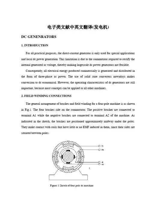
电子类文献中英文翻译(发电机)DC GENENRATORS1. INTRODUCTIONFor all practical purposes, the direct-current generator is only used for special applications and local dc power generation. This limitation is due to the commutator required to rectify the internal generated ac voltage, thereby making largescale dc power generators not feasible.Consequently, all electrical energy produced commercially is generated and distributed in the form of three-phase ac power. The use of solid state converters nowadays makes conversion to dc economical. However, the operating characteristics of dc generators are still important, because most concepts can be applied to all other machines.2. FIELD WINDING CONNECTIONSThe general arrangement of brushes and field winding for a four-pole machine is as shown in Fig.1. The four brushes ride on the commutator. The positive brusher are connected to terminal A1 while the negative brushes are connected to terminal A2 of the machine. As indicated in the sketch, the brushes are positioned approximately midway under the poles. They make contact with coils that have little or no EMF induced in them, since their sides are situated between poles.Figure 1 Sketch of four-pole dc matchineThe four excitation or field poles are usually joined in series and their ends brought out to terminals marked F1 and F2. They are connected such that they produce north and south poles alternately.The type of dc generator is characterized by the manner in which the field excitation is provided. In general, the method employed to connect the field and armature windings falls into the following groups (see Fig.2):Figure2 Field connections for dc generators:(a)separately excited generator;(b)self-excited,shunt generator;(c)series generator;(d)compound generator;short-shunt connection;(e)compoundgenerator,long-shunt connection.The shunt field contains many turns of relatively fine wire and carries a comparatively small current, only a few percent of rated current. The series field winding, on the other hand, has few turns of heavy wire since it is in series with the armature and therefore carries the load current.Before discussing the dc generator terminal characteristics, let us examine the relationship between the generated voltage and excitation current of a generator on no load. The generated EMF is proportional to both the flux per pole and the speed at which the generator is driven, EG=kn. By holding the speed constant it can be shown the EG depends directly on the flux.To test this dependency on actual generators is not very practical, as it involves a magnetic flux measurement. The flux is produced by the ampere-turns of the field coils: in turn, the flux must depend on the amount of field current flowing since the number of turns on the field winding is constant. This relationship is not linear because of magnetic saturation after the field current reaches a certain value. The variation of EG versus the field current If may be shown by a curve known as the magnetization curve or open-circuit characteristic. For this a given generator is driven at a constant speed, is not delivering load current, and has its field winding separately excited.The value of EG appearing at the machine terminals is measured as If is progressively increased from zero to a value well above rated voltage of that machine. The resulting curve is shown is Fig.3. When Ij=0, that is, with the field circuit open circuited, a small voltage Et is measured, due to residual magnetism. As the field current increases, the generated EMF increases linearly up to the knee of the magnetization curve. Beyond this point, increasing the field current still further causes saturation of the magnetic structure to set in.Figure 3 Magnetization curve or open-circuit characteristic of a separately excited dc machineThe means that a larger increase in field current is required to produce a given increase in voltage.Since the generated voltage EG is also directly proportional to the speed, a magnetization curve can be drawn for any other speed once the curve is determined. This merely requires anadjustment of all points on the curve according ton n x E E G G ''=where the quantities values at the various speeds.3. VOLTAGE REGULATIONLet us next consider adding a load on generator. The terminal voltage will then decrease (because the armature winding ha resistance) unless some provision is made to keep it constant. A curve that shows the value of terminal voltage for various load currents is called the load or characteristic of the generator.Figure 4 (a) directs current it to urge the generator load characteristics; (b) circuit diagramFig.4 shows the external characteristic of a separately excited generator. The decrease in the terminal voltage is due mainly to the armature circuit resistance RA. In general,A A G t R I E V -=where Vt is the terminal voltage and IA is the armature current (or load current IL) supplied by the generator to the load.Another factor that contributes to the decrease in terminal voltage is the decrease in flux due to armature reaction. The armature current established an MMF that distorts the main flux, resulting in a weakened flux, especially in noninterpole machines. This effect is calledarmature reaction. As Fig.4 shows, the terminal voltage versus load current curve does not drop off linearly since the iron behaves nonlinear. Because armature reaction depends on the armature current it gives the curve its drooping characteristic.4. SHUNT OR SELF-EXCIITED GENRATORSA shunt generator has its shunt field winding connected in parallel with the armature so that the machine provides its own excitation, as indicated in Fig.5. The question arises whether the machine will generate a voltage and what determines the voltage.For voltage to “build up” as it is called, there must be some remanent magnetism in the field poles. Ordinarily, if the generator has been used previously, there will be some remanent magnetism. We have seen in Section 3 that if the field would be disconnected, there will be small voltage Ef generated due to this remanent magnetism, provided that the generator is driven at some speed. Connecting the field for self-excitation, this small voltage will be applied to the shunts field and drive a small current through the field circuit. If this resulting small current in the shunt field is of such a direction that it weakens the residual flux, the voltage remains near zero and the terminal voltage does not build up. In this situation the weak main pole flux opposes the residual flux.Figure 5 Shunt generator:(a)circuit;(b)load characteristicIf the connection is such that the weak main pole flux aids the residual flux, the inducedvoltage increases rapidly to a large, constant value. The build-up process is readily seen to be cumulanve. That is, more voltage increases the field current, which in turn increases the voltage, and so on. The fact that this process terminates at a finite voltage is due to the nonlinear behavior of the magnctic circuit. In steady state the generated voltage is causes a field current to flow that is just sufficient to develop a flux required for the generated EMF that causes the field current to flow.The circuit carries only dc current, so that the field current depends only on the field circuit resistance, Rf. This may consist of the field circuit resistance Rf, the field current depends on the generated voltage in accordance with Ohm ’s law.It should be evident that on a new machine or one that has lost its residual flux because of a long idle period, some magnetism must be created. This is usually done by connecting the field winding only to a separate dc source for a few seconds. This procedure is generally known as flashing the field.Series GeneratorsAs mentioned previously, the field winding of a series generator is in series with the armature. Since it carries the load current the series field winding consists of only a few turns of thick wire. At no load, the generated voltage is small due to residual field flux only. When a load is added, the flux increases, and so does the generated voltage. Fig.7 shows the load characteristic of a series generator driven at a certain speed. The dashed line indicates the generated EMF of the same machine with the armature open-circuited and the field separately excited. The difference between the two curves is simply the IR drop in the series field and armature winding, such that)(S A A G t R R I E V +-=where RS is the series field winding resistance.Figure 7 Series generator: (a)circuit diagram;(b)load characteristicsCompound GeneratorsThe compound generator has both a shunt and a series field winding, the latter winding wound on top of the shunt winding. Fig.8 shows the circuit diagram. The two windings are usually connected such that their ampere-turns act in the same direction. As such the generator is said to be cumulatively compounded.The shunt connection illustrated in Fig.8 is called a long shunt connection. If the shunt field winding is directly connected across the armature terminals, the connection is referred to as a short shunt. In practice the connection used is of little consequence, since the shunt field winding carries a small current compared to the full-load current. Furthermore, the number of turns on the series field winding. This implies it has a low resistance value and the corresponding voltage drop across it at full load is minimal.Curves in Fig.9 represents the terminal characteristic of the shunt field winding alone. By the addition of a small series field winding the drop in terminal voltage with increased loading is reduced as indicated. Such a generator is said to be undercompounded. By increasing the number of series turns, the no-load and full-load terminal voltage can be made equal; the generator is then said to be flatcompounded. If the number of series turns is more than necessary to compensate for the voltage drop, the generator is overcome pounded. In that case the full-load voltage is higher than the no-load voltage.Figure 9 Terminal characteristics of compound generators compared with that of the shunt generatorThe overcompounded generator may be used in instances where the load is at some distance from the generator. The voltage drops in the feeder lines are the compensated for with increased loading. Reversing the polarity of the series field in relation to the shunt field, the fields will oppose each other more and more as the load current increase. Such a generator is said to be differentially compounded. It is used in applications where feeder lines could occur approaching those of a short circuit. An example would be where feeder lines could break and short circuit the generator. The short-circuit current, however, is then limited to a “safe” value. The terminal characteristic for this type of generator is also shown in Fig.9. Compound generators are used more extensively than the other types because they may be designed to have a wide varity of terminal characteristics.As illustrated, the full-load terminal voltage can be maintained at the no-load value by the proper degree of compounding. Other methods of voltage control are the use of rheostats, for instance, in the field circuit. However, with changing loads it requires a constant adjustment of the field rheostat to maintain the voltage. A more useful arrangement, which is now common practice, is to use an automatic voltage regulator with the generator. In essence, the voltage regulator is a feedback control system. The generator output voltage is sensed and compared to a fixed reference voltage deviation from the reference voltage gives an error signal that is fed to a power amplifier. The power amplifier supplies the field excitation current. If the error signal is positive, for example, the output voltage is larger than desiredand the amplifier will reduce its current drive. In doing so the error signal will be reduced to zero.TRANSFORMER1. INTRODUCTIONThe high-voltage transmission was need for the case electrical power is to be provided at considerable distance from a generating station. At some point this high voltage must be reduced, because ultimately is must supply a load. The transformer makes it possible for various parts of a power system to operate at different voltage levels. In this paper we discuss power transformer principles and applications.2. TOW-WINDING TRANSFORMERSA transformer in its simplest form consists of two stationary coils coupled by a mutual magnetic flux. The coils are said to be mutually coupled because they link a common flux. In power applications, laminated steel core transformers (to which this paper is restricted) are used. Transformers are efficient because the rotational losses normally associated with rotating machine are absent, so relatively little power is lost when transforming power from one voltage level to another. Typical efficiencies are in the range 92 to 99%, the higher values applying to the larger power transformers.The current flowing in the coil connected to the ac source is called the primary winding or simply the primary. It sets up the flux φ in the core, which varies periodically both in magnitude and direction. The flux links the second coil, called the secondary winding or simply secondary. The flux is changing; therefore, it induces a voltage in the secondary by electromagnetic induction in accordance with Lenz’s law. Thus the primary receives its power from the source while the secondary supplies this power to the load. This action is known as transformer action.3. TRANSFORMER PRINCIPLESWhen a sinusoidal voltage V p is applied to the primary with the secondary open-circuited, there will be no energy transfer. The impressed voltage causes a small current Iθ to flow in the primary winding. This no-load current has two functions: (1) it produces the magnetic flux in the core, which varies sinusoidally between zero and φm, where φm is the maximum value of the core flux; and (2) it provides a component to account for the hysteresis and eddy current losses in the core. There combined losses are normally referred to as the core losses.The no-load current Iθ is usually few percent of the rated full-load current of the transformer (about 2 to 5%). Since at no-load the primary winding acts as a large reactance due to the iron core, the no-load current will lag the primary voltage by nearly 90º. It is readily seen that the current component I m= I0sinθ0, called the magnetizing current, is 90ºin phase behind the primary voltage V P. It is this component that sets up the flux in the core; φ is therefore in phase with I m.The second component, I e=I0sinθ0, is in phase with the primary voltage. It is the current component that supplies the core losses. The phasor sum of these two components represents the no-load current, orI0 = I m+ I eIt should be noted that the no-load current is distortes and nonsinusoidal. This is the result of the nonlinear behavior of the core material.If it is assumed that there are no other losses in the transformer, the induced voltage In the primary, E p and that in the secondary, E s can be shown. Since the magnetic flux set up by the primary winding,there will be an induced EMF E in the secondary winding in accordance with Faraday’s law, namely, E=NΔφ/Δt. This same flux also links the primary itself, inducing in it an EMF, E p. As discussed earlier, the induced voltage must lag the flux by 90º, therefore, they are 180º out of phase with the applied voltage. Since no current flows in the secondary winding, E s=V s. The no-load primary current I0 is small, a few percent of full-load current. Thus the voltage in the primary is small and V p is nearly equal to E p. The primary voltage and the resulting flux are sinusoidal; thus the induced quantities E p and E s vary as a sine function. The average value of the induced voltage given byE avg = turns× change in flux in a given time given timewhich is Faraday’s law applied to a finite time interval. It follows thatE avg = N 21/(2)m f = 4fNφm which N is the number of turns on the winding. Form ac circuit theory, the effective or root-mean-square (rms) voltage for a sine wave is 1.11 times the average voltage; thusE = 4.44fNφmSince the same flux links with the primary and secondary windings, the voltage per turn in each winding is the same. HenceE p = 4.44fN p φmandE s = 4.44fN s φmwhere E p and Es are the number of turn on the primary and secondary windings, respectively. The ratio of primary to secondary induced voltage is called the transformation ratio. Denoting this ratio by a, it is seen that a = p sE E = p s N N Assume that the output power of a transformer equals its input power, not a bad sumption in practice considering the high efficiencies. What we really are saying is that we are dealing with an ideal transformer; that is, it has no losses. ThusP m = P outorV p I p × primary PF = V s I s × secondary PFwhere PF is the power factor. For the above-stated assumption it means that the power factor on primary and secondary sides are equal; thereforeV p I p = V s I s from which is obtainedp s V V = p s I I ≌ p sE E ≌ aIt shows that as an approximation the terminal voltage ratio equals the turns ratio. The primary and secondary current, on the other hand, are inversely related to the turns ratio. The turns ratio gives a measure of how much the secondary voltage is raised or lowered in relation to the primary voltage. To calculate the voltage regulation, we need more information.The ratio of the terminal voltage varies somewhat depending on the load and its power factor. In practice, the transformation ratio is obtained from the nameplate data, which list the primary and secondary voltage under full-load condition.When the secondary voltage V s is reduced compared to the primary voltage, the transformation is said to be a step-down transformer: conversely, if this voltage is raised, it is called a step-up transformer. In a step-down transformer the transformation ratio a is greater than unity (a>1.0), while for a step-up transformer it is smaller than unity (a<1.0). In the event that a=1, the transformer secondary voltage equals the primary voltage. This is a special type of transformer used in instances where electrical isolation is required between the primary and secondary circuit while maintaining the same voltage level. Therefore, this transformer is generally knows as an isolation transformer.As is apparent, it is the magnetic flux in the core that forms the connecting link between primary and secondary circuit. In section 4 it is shown how the primary winding current adjusts itself to the secondary load current when the transformer supplies a load.Looking into the transformer terminals from the source, an impedance is seen which by definition equals V p / I p . From p s V V = p s I I ≌ p sE E ≌ a , we have V p = aV s and I p = I s /a.In terms of V s and I s the ratio of V p to I p isp p V I = /s s aV I a= 2s s a V I But V s / I s is the load impedance Z L thus we can say thatZ m (primary) = a 2Z LThis equation tells us that when an impedance is connected to the secondary side, it appears from the source as an impedance having a magnitude that is a 2 times its actual value. We say that the load impedance is reflected or referred to the primary. It is this property oftransformers that is used in impedance-matching applications.4. TRANSFORMERS UNDER LOADThe primary and secondary voltages shown have similar polarities, as indicated by the “dot-making” convention. The dots near the upper ends of the windings have the same meaning as in circuit theory; the marked terminals have the same polarity. Thus when a load is connected to the secondary, the instantaneous load current is in the direction shown. In other words, the polarity markings signify that when positive current enters both windings at the marked terminals, the MMFs of the two windings add.Since the secondary voltage depends on the core flux φ0, it must be clear that the flux should not change appreciably if E s is to remain essentially constant under normal loading conditions. With the load connected, a current I s will flow in the secondary circuit, because the induced EMF E s will act as a voltage source. The secondary current produces an MMF N s I s that creates a flux. This flux has such a direction that at any instant in time it opposes the main flux that created it in the first place. Of course, this is Lenz’s law in action. Thus the MMF represented by N s I s tends to reduce the core flux φ0. This means that the flux linking the primary winding reduces and consequently the primary induced voltage E p, This reduction in induced voltage causes a greater difference between the impressed voltage and the counter induced EMF, thereby allowing more current to flow in the primary. The fact that primary current I p increases means that the two conditions stated earlier are fulfilled: (1) the power input increases to match the power output, and (2) the primary MMF increases to offset the tendency of the secondary MMF to reduce the flux.In general, it will be found that the transformer reacts almost instantaneously to keep the resultant core flux essentially constant. Moreover, the core flux φ0drops very slightly between n o load and full load (about 1 to 3%), a necessary condition if E p is to fall sufficiently to allow an increase in I p.On the primary side, I p’ is the current that flows in the primary to balance the demagnetizing effect of I s. Its MMF N p I p’ se ts up a flux linking the primary only. Since the core flux φ0 remains constant. I0 must be the same current that energizes the transformer at no load. Theprimary current I p is therefore the sum of the current I p’ and I0.Because the no-load current is relatively small, it is correct to assume that the primary ampere-turns equal the secondary ampere-turns, since it is under this condition that the core flux is essentially constant. Thus we will assume that I0 is negligible, as it is only a small component of the full-load current.When a current flows in the secondary winding, the resulting MMF (N s I s) creates a separate flux, apart from the flux φ0 produced by I0, which links the secondary winding only. This flux does no link with the primary winding and is therefore not a mutual flux.In addition, the load current that flows through the primary winding creates a flux that links with the primary winding only; it is called the primary leakage flux. The secondary- leakage flux gives rise to an induced voltage that is not counter balanced by an equivalent induced voltage in the primary. Similarly, the voltage induced in the primary is not counterbalanced in the secondary winding. Consequently, these two induced voltages behave like voltage drops, generally called leakage reactance voltage drops. Furthermore, each winding has some resistance, which produces a resistive voltage drop. When taken into account, these additional voltage drops would complete the equivalent circuit diagram of a practical transformer. Note that the magnetizing branch is shown in this circuit, which for our purposes will be disregarded. This follows our earlier assumption that the no-load current is assumed negligible in our calculations. This is further justified in that it is rarely necessary to predict transformer performance to such accuracies. Since the voltage drops are all directly proportional to the load current, it means that at no-load conditions there will be no voltage drops in either winding.中文翻译①直流发电机1.介绍关于所有实际目的来说,直流发电机仅用于特殊场合与地方性发电厂。
中英文对照外文翻译文献(文档含英文原文和中文翻译)外文文献:Circuit BreaksWithin a few years of the introduction of the fuse,the growing electrical industry started looking for an alternative method of providing protection for electric circuits.They wanted a device that would not bedestroyed by its operation,that could simply be reset to restore power, and that could also be used as a means of switching for the circuit.Out of this development work came the circuit breaker.which is an electromechanical device.The circuit breaker is defined as a device designed to open and close a circuit by non-automatic means and to open the circuit automatically on a predetermined over-current without injure to itself when properly applied within its rating.As with other equipment,circuit breakers are divided into those rated for 1 000 volts and less and those rated for more than 1000 volts.Low-voltage circuit breakers were also divided into two distinct categories,molded-case and power types.However,in the past few years the distinction between these two types has become less clea-cut as a new type of encased breaker are universally operated in air, so it is not necessary to designate them as air circuit breakers as this understood.Medium and high—voltage breakers,on the other hand,use mediums other than air in which to open the circuit and therefore must be designated as being air, gas,and so on.Apart from having different voltage and continuous currentratings.breakers have widely different interrupting ratings,response characteristics,and methods of operation.The proper application of circuit breakers requires a good knowledge of all the characteristics and options available for each type.The simplest circuit—opening device is the manually operated knife switch.This switch has the basic parts required of any circuit—opening device:a fixed contact, a moving,an operating handle,and a base—plate or flame.However as anyone who has opened a knife switch under load has witnessed,there is a luminous discharge drawn between the separating contacts of the switch.This discharge is called an arc,and it consists of a stream of positive and negative ions. The current flowing in a circuit cannot be instantaneously interrupted.As a result,the arc continues until the switch contacts have separated far enough to finally extinguish the arc.The arc can make the opening of the switch very unsafe and unreliable when interrupting a circuit breaker must provide a safer and more reliable interrupting action. The following are the means by witch low—voltage circuit breakers can be made to safely interrupt large faultcurrents with a minimum of contact damage.1.Fast speed of operation.The duration and severity of an arc depends in part on the speed with witch the contacts can be separated,therefore powerful spring are used to rapidly force the contacts open.These springs are compressed (charged)during the closing operation.The breaker contacts are then mechanically held closed and are released by a separate trip mechanism.An operator can initiate the opening of the breaker but has no control over the speed with which the contacts separate.2.Use of arcing contacts.The arc burn can cause pitting,which eventually affects the ability of the contacts to carry the load current when closed.To offset this, two parallel sets of contacts are used for each pole of the breaker,a main current carrying set and an auxiliary or arcing set.When the breaker is tripped open, the main contacts separate first,transferring the current flow to the arcing contacts.The arcing contacts then separate a split second late,drawing the arc between them and leaving the main contacts free of any arcing.This allows the surfaces of the main current carrying contacts to be made of high—conductivitymetal such as silver,the surfaces of the arcing contacts are then made of a tougher alloy better able to withstand the effects of arcing.3.Use of arc chutes Parallel plates enclosed in the form of a chute are mounted directly above the arcing contacts.As the arcing contacts separate, the resulting are creates a strong magnetic field that forces the arc upward into the plates.The arc stream is then broken into a series of small arcs,which are quickly cooled,deionized,and extinguished.The ionized gases created by the are stream must be deionized before they are expelled from the arc chute;otherwise,secondary arcing could occur between the line side terminals of the breaker, which are still energized.中文译文:断路器在引入保险丝的这几年,电气行业开始寻找一种保护电路的替代方法。
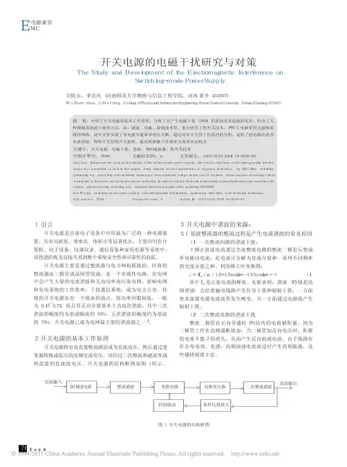
开关电源电磁干扰及抑制本文分析了开关电源中电磁干扰产生的原因和传播的路径。
通过减小干扰源产生的干扰和切断干扰传播路径的方法,提出了抑制干扰的有效措施,并重点介绍了变压器的设计方法和制作方法。
关键词:开关电源;电磁干扰;仰制Electromagnetic interference and suppression of switching power supplyAuthor: Sun Ruilong, Wang XiaokeAuthor: WuSitai thermal power plant of Inner Mongolia Energy Power Investment Group Co., LtdThis paper analyzes the cause of EMI in switching power supply and its propagation path. By reducing the interference of interference source and cutting off the path of interference propagation, the effective measures of interference suppression are put forward, and the design method and manufacturing method of transformer are mainly introduced.Key words: switching power supply; electromagnetic interference; inverted system1 绪论1.1 课题的背景及意义由于开关电源工作在高频开关状态,内部会产生很高的电流、电压变化率(即高dv/dt和di/dt),导致开关电源产生较强的电磁干扰(EMI,Electro Magnetic Interference)。
高速铁路弓网电弧电磁干扰论文中英文资料外文翻译附录A(原文)A Simulation of Arc Generation at AC-DC Neutral Section of Electric RailwayYoungsoo Han, Kyuhyoung ChoiAbstract--This paper provides an experimental and theoretical analysis of the arc discharges generated between contact wire and pantograph of high speed railway.A video-based arc detection device is installed on the KTX train, and arc discharges are measured for a 45.87km track section of high speed railway in Korea. It is measured that the rate of contact loss is 0.3% which is lower than the regulated value of 1.0% for high speed train, and arc discharges induced by 21 small size contact losses and 6 medium size contact losses occur continuously along the track. The power of arc discharge between contact wire and pantograph is calculated as 9.0~22.5[kW] which is approximately one-hundredth of that of the arc discharges generated at the neutral section of contact wire. The results of the measurement and the analysis suppose that a study be followed to suppress arc discharges and contact wire damages for the safe operation of high speed railway.Index Terms—Electric railway;arc discharge;contact loss;contact wire; pantograph;neutral section.I.NOMENCLATURES/S : Sub-Station of Electric RailwaySP : Sectioning PostSSP : Sub- Sectioning PostAT : Auto-TransformerTF : Trolley FeederAF : Auto- Transformer FeederFPW : Fault Protective WireNW : Neutral WireNS : Neutral SectionCCTV: Closed Circuit TelevisionEMI: Electromagnetic InterferenceLAN: Local Area NetworkMCB: Main Circuit BreakerKTX: Korea Train ExpressII.INTRODUCTIONCatenary systems play a important role in supplying electric power without interruption to trains moving fast. The pantographs installed on train collect currents for traction while keeping in contact with the catenary system. Arc discharges occur between the contact wire and the pantographs, when the pantographs happen to lose contact with the contact wire.Arc discharge also occurs when the train passes through the AC-DC neutral section of the catenary system where electricity is not supplied. These arc discharges give rise to many problems such as spoiling the contact wire and the pantographs,and inducing EMI phenomena,audible noises and other environmental pollutions.Arc discharges generally have large heating power which may spoil the slider of pantograph made of sintered alloy and even breaks the contact wires.V oltage surges induced by arc discharges may produce EMI problems to the small size environment or mal-operation of electronic devices on the train. The damages caused by arc discharge will be more critical for high speed railway.The faster train moves,the more difficult to keeping in contact with catenary for pantograph. Moreover, as train speeds up, the train traction currents should be increased,which inevitably give rise to larger arc discharges.This paper provides an experimental and theoretical analysis of the arc discharges generated between the contact wire and the pantograph of high speed railway. A designated arc detection device is installed on the KTX train, and arc discharges are measured for a 45.87[km] track section of high speed railway.Arc generation frequency, arc current and arc size is measured along the track.A data analysis and an arc power model is suggested too.III. ARC DISCHARGES BETWEEN CONTACT WIRE ANDPANTOGRAPHThe power supply system of electric railway consists of S/S and catenary system.S/S converts three phase 154[kV] electric power to single phase 25[kV] being suitable for supplying to train.High speed railway adopts AT feeding system which can supply large electric power for long distance as shown in Fig. 1. The S/S supplies AC 50[kV] to AT, and AT supply AC 25[kV] to train. The converted electric power is supplied to train by way of the catenary system which is composed of a contact wire,a messenger wire and hangers.The main purpose of the catenary system is to supply electric power without interruption to trains moving fast.The pantographs installed on train collect electric power while contacting the contactwire of the catenary system.Fig. 2. Shows the configuration of the catenary system. The pantograph is connected to the contact wire by its lift force against the contact wire. Contact wires supported by hangers and supporting structures has uneven stiffness points which give rise to contact losses.Moreover,as train speed up,contact loss happens more frequently.Arc discharges occur between the contact wire and the pantographs, when the pantographs happen to lose contact with the contact wire.The contact loss phenomena are classified into three groups according to their duration; small size, medium size and large size. Small size contact loss is induced by delicate vibration of pantograph,and continues for several tenths of a second. Medium size contact losses occur when trains pass through the uneven stiff point of the contact wire, and continues for a second and below. Large size contact losses, continuing for several seconds,are induced by jumping movements of pantograph after passing through bracket supporting points of contact wire.Contact wires have several neutral sections insulated from other parts of contact wires,in other words dead sections,which divide the sections having different phases and different supply voltages such as AC 25,000[V] or DC 1,500[V]. Trains should go into the neutral sections after making notch-off operation whichbreaks the train current by MCB, otherwise the train current is interrupted by the neutral section which result in a large arc discharge between the contact wire and the pantograph as shown in Fig. 2.This arc discharge also happens when train go into the voltage-supplied section from the neutral section.IV.MEASUREMENT OF CONTACT LOSS BETWEEN CONTACTWIRE AND PANTOGRAPHA.Measurement deviceFig. 4. Shows the system block diagram of arc measurement device.The device, installed on the KTX train moving at the speed of 300[km/h],measures contact force between contact wire and pantograph,vibration acceleration of pantograph, and the shape of arc discharge.Strain gauges are installed on the bow and arms of pantograph to measure the acceleration and contact force.Table 1 shows the specifications of the sensors.The image of arc discharge is captured by CCTV camera activated by arc detection sensor.Fig. 5 shows a captured image of arc discharge. All the data measured by on-board device are transmitted to wayside server via wireless LAN.B.Measurement data analysisThe measurement has been carried out at the 45.78[km] track section of high speed railway with 300[km/h] train operation. Table 2 shows the results of the measurement; time, location of arc discharge,arc strength,the length of contact loss, train speed,arc current,and pantograph voltage.Fig. 6 show a train speed profile with voltage and current distributions.While KTX train moves on the 45.78[km] track section, 21 small size contact losses and 6 medium size contact losses are observed and rge size contact loss was not detected at the experiment. The rate of contact loss is defined as;rate of contact loss = sum of contact loss time ×100[%] (1)total operation timeKorean railroad corporation suggests the rate of contact loss for high speed railway should be lower than 1.0[%]. Based on the measured data in Table 2,the rate of contact loss is calculated as 0.31[%], which means the catenary system and the pantograph of KTX fulfill the regulation in Korea. Nevertheless, it should be noted that some arc discharges are occurring continuously during the high speed operation of KTX.C. Modeling of arc dischargeThe instantaneous power of arc discharge is described by arc voltage va , and arc current i as follows,i v p a ⋅= (2) The average power of arc discharge can be calculated by integrating over the period T.⎰⎰⋅⋅=⋅⋅=T a T idt v T pdt T P 0011 (3) It is reported that the voltage and current of arc discharge at AC circuit have the waveforms shown in Fig.7[8].The arc voltage has constant value V during half the period, depicted by square wave. Thus, the equation(3) for average power of arc discharge can be simplified by setting va = Va .The current wave form of AC arc discharge in Fig. 7 is approximately sinusoidal having some harmonic.Neglecting the harmonics which is evaluated as several hundredths of fundamental wave, arc current can be approximated ast I i ωsin 2= (5) Consequently, the average power isI V tdt I T V P a Ta 9.0sin 210=⋅=⎰ω (6)Where I is effective value of AC current, and V is arc voltage that can be measured by voltmeter.The arc discharge between contact wire and pantograph has the followingcharacteristics. Arc currents are very large up to 500[A].Arc discharge between contact wire and pantograph can be simulated by arc discharge between bar and plate. Fig.8 shows a typical voltage-current characteristics of high current arc discharge between bar and plate. As the arc current is 500[A] in Table 2, arc voltage can be estimated as 20~50[V] according to displacement between contact wire and pantograph from Fig. 8. Thus, the power of arc discharge between contact wire and pantograph is calculated to be 9.0~22.5[kV A] by equation (6). The power of arc discharge between contact wire and pantograph is approximately one-hundredth of that of the arc discharges generated at the neutral section of contact wire.V. CONCLUSIONArc discharges between the contact wire and pantograph have been measured on the KTX train along 45.87km track using a video-based arc detection device. Although the rate of contact loss is measured as 0.3% which is lower than the regulated value of 1.0%,arc discharges occurs continuously along the track induced by 21 small size contact losses and 6 medium size contact losses.The power of arc discharge between contact wire and pantograph is calculated as 9.0~22.5[kW] which is approximately one-hundredth of that of the arc discharges generated at the neutral section of contact wire.The results reveal that the study be followed to suppress arc discharges and contact wire damages for the safe operation of high speed train.附录A(译文)电力机车交-直分相装置上产生电弧的仿真实验Youngsoo Han, Kyuhyoung Choi摘要---本文提供了一个实验和理论分析了高速铁路中接触网和受电弓之间产生的电弧放电现象。
Switching Power Supply目录1 Switching Power Supply (1)Linear versus Switching Power Supplies (1)Basic Converters (2)1.2.1Forward-Mode Converter Fundamentals (2)1.2.3 Flyback or Boost-mode Converter Fundamentals (4)1.3 Topologies (5)1 开关电源 (7)1.1 线性电源和开关电源之比拟 (7)根本转换器 (8)1.2.1 前向模式转换器根底 (8)12.2 增压模式转换器根底 (8)1.3 拓扑结构 (9)2 Operational Amplifiers (10)2 放大器 (14)1 Switching Power SupplyEvery new electronic product , except those that battery powered, requires converting off-line 115V ac or 230V ac power to some dc voltage for powering the electronics. Efficient conversion of electrical power is becoming a primary concern to companies and to society as a whole.Switching power supplies offer not only higher efficiencies but also offer greater flexibility to the designer. Recent advances in semiconductor, magnetic and passive technologies make the switching power supply an ever more popular choice in the power conversion arena today.1.1 Linear versus Switching Power SuppliesHistorically, the linear regulator was the primary method of creating a regulated output voltage. It operates by reducing a higher input voltage down to the lower output voltage by linearly controlling the conductivity of a series pass power device in response to changes in its load. This results in a large voltage being placed across the pass unit with the load current flowing through it.This headroom loss ()V I⨯ causes the linear regulator to only be 30 todrop load50 percent efficient. That means that for each watt delivered to the load , at least a watt has to be dissipated in heat. The cost of the heatsink actually makes the linear regulator uneconomical above 10watts for small applications. Below that point, however, they are cost effective in step-down applications.The switching regulator operates the power devices in the full-on and cutoff states. This then results in either large currents being passed through the power devices with a low“on〞voltage or no current flowing with high voltage across the device. This results in a much lower power being dissipated within the supply.The average switching power-supply exhibits efficiencies of between 70 to 90 percent, regardless of the input voltage.Higher levers of integration have driven the cost of switching power supplies downward which makes in an attractive choice for output powers greater than 10 watts or where multiple outputs are desired.1.2 Basic ConvertersForward-Mode Converter FundamentalsThe most elementary forward-mode converter is the Buck or Step-down Converter which can be seen in Figure 3.1.Its operation can be seen as having two distinct time periods which occur when the series power switch is on and off. When the power switch is on ,the inputvoltage is connected to the input of the inductor .The output of switch of inductor is the output voltage, and the rectifier is back-biased. During this period, since there is a constant voltage source connected across the inductor, the inductor current begins to linearly ramp upward which is described by:()()in out on L on V V t i L -⨯=During the “on 〞 period , energy is being stored within the core material of the inductor in the form of flux. There is sufficient energy stored to carry the requirements of the load during the next off period.The next period is the “off 〞 period of the power switch .When the power switch turns off, the input voltage of the inductor flies below ground and is clamped at one diode drop below ground by the catch diode. Current now begins to flow through the catch diode thus maintaining the load current loop. This remove the stored energy from the inductor, The inductor. The inductor current during this time is:()()out D offL off V V t i L -⨯=This period ends when the power switch is once again turned on.Regulation is accomplished by varying the on-to-off duty cycle of the power switch. The relationship which approximately describes its operation is:out in V V ≈∂⨯Where ∂ is the duty cycle (()/on on off t t t ∂=+).The buck converter is capable of kilowatts of output power, but suffers from one serious shortcoming which would occur if the power switch were to fail short-circuited, the input power source is connected directly to the load circuitry with usually produces catastrophic results. To avoid this situation, a crowbar is placed across the output. A crowbar is a latching SCR which is fired when the output is sensed as entering an overvoltage condition. The buckconverter should only be used for board-level regulation.Flyback or Boost-mode Converter FundamentalsThe most elementary flyback-mode converter is the boost or Step-up Converter. Its schematic can be seen in Figure3.2.Its operation can also be broken into two distinct periods where the power switch is on or off. When power switch turns on, the input voltage source is placed directly across the inductor. This causes the current to begin linearly ramping upwards from zero and is described by:()in on L on V t i L ⨯=Once again, energy is being stored during each cycle times the frequency of operation must b higher than the power demands of the load or,20.5sto pkop out P L I f P =⨯⨯>The power switch then turns off and the inductor voltage flies back abovethe input voltage and is clamped and is clamed by the rectifier at the output voltage .The current then begins to linearly ramp downward until the until the energy within the core is completely depleted. Its waveform which is shown in Figure 3.3 is determined by:()()out in offL off V V t i L -⨯=The boost converter should also be only used for board-level regulation.1.3 TopologiesA topology is the arrangement of the power devices and their magnetic elements. Each topology has its own merits within certain applications. Some of the factors which determine the suitability of a particular topology to a certain application are:1) Is the topology electrically isolated from the input to the output or not.2) How much of the input voltage is placed across the inductor or transformer.3) What is the peakcurrent flowing through the power semiconductors.4) Are multiple outputs required.5) How much voltage appears across the power semiconductors.The first choice that faces the designer is whether to have input to output transformer isolation. Non-isolated switching power supplies are typically used for board-level regulation where a dielectric barrier is provided elsewhere within the system. Non-isolated topologies should also be used where the possibility of a failure does not connect the input power source to the fragile load circuitry. Transformer isolation should be used in all other situations. Associated with that is the need for multiple output voltages. Transformers provide an easy method for adding additional output voltage to the switching power supply. The companies building their own power systems are leaning toward transformer isolation in as many power supplies as possible since it prevents a domino effect during failure conditions.1 开关电源除了那些用电池做电源的电子产品外,每个新型电子产品都需要将115V或者230V 的交流电源转换为直流电源,为电路供电。
电气工程及其自动化外文翻译外文文献英文文献短路电流Short-circuit current1 Terms and DefinitionsThe following terms and definitions correspond largely to those defined in IEC 60909. Refer to this standard for all terms not used in this book.The terms short circuit and ground fault describe faults in the isolation ofoperational equipment which occur when live parts are shunted out asa result. , Causes:1. Overtemperatures due to excessively high overcurrents.2. Disruptive discharges due to overvoltages.3. Arcing due to moisture together with impure air, especially on insulators. , Effects:1. Interruption of power supply.2. Destruction of system components.3. Development of unacceptable mechanical and thermal stresses in electrical operational equipment., Short circuit:According to IEC 60 909, a short circuit is the accidental or intentional conductive connection through a relatively low resistance orimpedance between two or more points of a circuit which are normally at different potentials., Short circuit current:According to IEC 60 909, a short circuit current results from a short circuit in an electrical network.It is necessary to differentiate here between the short circuit current at the position of the short circuit and the transferred short circuit currents in the network branches., Initial symmetrical short circuit current:This is the effective value of the symmetrical short circuit current at the moment at which the short circuit arises, when the short circuit impedance has its value from the time zero., Initial symmetrical short circuit apparent power:The short circuit power represents a fictitious parameter. During the planning of networks, the short circuit power is a suitable characteristic number. , Peak short circuit current:The largest possible momentary value of the short circuit occurring. , Steady state short circuit current:Effective value of the initial symmetrical short circuit current remaining after the decay of all transient phenomena., DC aperiodic component:Average value of the upper and lower envelope curve of the short circuit current, which slowly decays to zero., Symmetrical breaking current:Effective value of the short circuit current which flows through the contact switch at the time of the first contact separation., Equivalent voltage source:The voltage at the position of the short circuit, which is transferred to the positive-sequence system as the only effective voltage and is used for the calculation of the short circuit currents., Superposition method:The superposition method considers the previous load of the network before the occurrence of the short circuit. It is necessary to know the load flow and the setting of the transformer step switch., Voltage factor:Ratio between the equivalent voltage source and the network voltage Un,divided by 3., Equivalent electrical circuit:Model for the description of the network by an equivalent circuit. , Far-from-generator short circuit:The value of the symmetrical AC periodic component remains essentially constant., Near-to-generator short circuit:The value of the symmetrical AC periodic component does not remain constant. The synchronous machine first delivers an initial symmetrical short circuit current which is larger than twice the rated current of the synchronous machine. , Positive-sequence short circuit impedance:The impedance of the positive-sequence system as seen from the position of theshort circuit., Negative-sequence short circuit impedance:The impedance of the negative-sequence system as seen from the position ofthe short circuit., Zero-sequence short circuit impedanceThe impedance of the zero-sequence system as seen from the position of theshort circuit. Three times the value of the neutral point to ground impedanceoccurs here., Short circuit impedance:Impedance required for calculation of the short circuit currents at the positionof the short circuit. p•••1.2 Short circuit path in the positive-sequence systemFor the same external conductor voltages, a three-pole short circuit allows three currents of the same magnitude to develop between the three conductors. It is therefor only necessary to consider one conductor in further calculations. Depending on the distance from the position of the short circuit from the generator, here it is necessary to consider near-to-generator andfar-from-generator short circuits separately. For far-from-generator and near-to-generator short circuits, the short circuit path can be represented by a mesh diagram with AC voltage source, reactances X and resistances R (Figure 1.2). Here, X and R replace all components such as cables,conductors, transformers, generators and motors.Fig. 1.2: Equivalent circuit of the short circuit current path in the positive-sequence systemThe following differential equation can be used to describe theshort circuit processwhere w is the phase angle at the point in time of the short circuit. This assume that the current before S closes (short circuit) is zero. The inhomogeneous first order differential equation can be solved by determining the homogeneous solution ik and a particular solution i?k.The homogeneous solution, with the time constant g = L/R, solution yields:For the particular solution, we obtain:The total short circuit current is composed of both components:The phase angle of the short circuit current (short circuit angle)is then, in accordance with the above equation,For the far-from-generator short circuit, the short circuit current is therefore made up of a constant AC periodic component and the decaying DC aperiodic component. From the simplified calculations, we can now reach the following conclusions:, The short circuit current always has a decaying DC aperiodic component inaddition to the stationary AC periodic component., The magnitude of the short circuit current depends on theoperating angle ofthe current. It reaches a maximum at c = 90 (purely inductive load). Thiscase serves as the basis for further calculations., .The short circuit current is always inductive.1.4 Methods of short circuit calculationThe equivalent voltage source will be introduced here as the only effective voltage of the generators or network inputs for thecalculation of short circuit currents. The internal voltages of generators or network inputs are short circuited, and at the position ofthe short circuit (fault position) the value ( is used as the only effective voltage (Figure 1.4)., The voltage factor c [5] considers (Table 1.1):, The different voltage values, depending on time and position, The step changes of the transformer switch, That the loads and capacitances in the calculation of the equivalentvoltage source can be neglected, The subtransient behavior of generators and motors, This method assumes the following conditions:, The passive loads and conductor capacitances can be neglected , The step setting of the transformers do not have to be considered , The excitation of the generators do not have to be considered , The time and position dependence of the previous load (loading state) ofthe network does not have to be consideredFig. 1.4: Network circuit with equivalent voltage sourcea) three-phase network, b) equivalent circuit in positive sequencesystem1.4.2 Superposition methodThe superposition method is an exact method for the calculation of the short circuit currents. The method consists of three steps. The voltage ratios and the loading condition of the network must be known before the occurrence of the short circuit. In the first step the currents, voltages and the internal voltages for steady-state operation before onset of the short circuit are calculated (Figure 1.5b). The calculation considers the impedances, power supply feeders and node loads of the active elements. In the second step the voltage applied to the fault location before the occurrence of the short circuit and the current distribution at the fault location are determined with a negative sign (Figure 1.5c). This voltage source is the only voltage source in the network. The internal voltages are short-circuited. In the third step both conditions are superimposed. We then obtain zero voltage at the fault location. The superposition of the currents also leads to the value zero. The disadvantage of this method is that the steady-state condition must be specified. The data for the network (effective andreactive power, node voltages and the step settings of the transformers) are often difficult to determine. The question also arises, which operating state leads to the greatest short circuit current. Figure 1.5 illustrates the procedure for the superposition method.Fig. 1.5: Principle of the superposition methoda) undisturbed operation, b) operating voltage at the faultlocation, c) superposition of a) and b)1.4.3 Transient calculationWith the transient method the individual operating equipment and, as a result, the entire network are represented by a system of differential equations. The calculation is very tedious. The method with the equivalent voltage source is a simplification relative to the other methods. Since 1988, it has been standardized internationally in IEC 60 909. The calculation is independent of a current operational state. Inthisbook, we will therefore deal with and discuss the method with the equivalent voltage source.1.5 Calculating with reference variablesThere are several methods for performing short circuit calculations with absolute and reference impedance values. A few are summarized here and examples are calculated for comparison. To define the relative values, there are two possible reference variables.For the characterization of electrotechnical relationships we require the four parameters:, Voltage U in V, Current I in A, Impedance Z in W, Apparent power S in VA.Three methods can be used to calculate the short circuit current:1. The Ohm system: Units: kV, kA, V, MVA2.The pu system:This method is used predominantly for electrical machines; allfour parameters u, i, z and s are given as per unit (unit = 1). The reference valueis 100 MVA. The two reference variables for this system are UB and SB.Example: The reactances of a synchronous machine Xd, X?d, X?d are givenin pu or in % pu, multiplied by 100 %.3.The %/MVA system:This system is especially well suited for thefastdetermination of short circuit impedances. As formal unit only the % symbol isadd.短路电流1 术语和定义以下术语和定义对应IEC 标准60 909。
中英文对照外文翻译(文档含英文原文和中文翻译)英文:Intelligent switch power supplyWith the rapid development of electronic technology, application field of electronic system is more and more extensive, electronic equipment, there are more and more people work with electronic equipment, life is increasingly close relationship. Any electronic equipment are inseparable from reliable power supply for power requirements, they more and more is also high. Electronic equipment miniaturized and low cost in the power of light and thin, small and efficient for development direction. The traditional transistors series adjustment manostat is continuous control linear manostat. This traditional manostat technology more mature, and there has been a large number of integrated linear manostat module, has the stable performance is good, output ripple voltage small, reliable operation, etc. But usually need are bulky and heavy industrial frequency transformer and bulk and weight are big filter.In the 1950s, NASA to miniaturization, light weight as the goal, for a rocket carrying the switch power development. In almost half a century of developmentprocess, switch power because of its small volume, light weight, high efficiency, wide range, voltage advantages in electric, control, computer, and many other areas of electronic equipment has been widely used. In the 1980s, a computer is made up of all of switch power supply, the first complete computer power generation. Throughout the 1990s, switching power supply in electronics, electrical equipment, home appliances areas to be widely, switch power technology into the rapid development. In addition, large scale integrated circuit technology, and the rapid development of switch power supply with a qualitative leap, raised high frequency power products of, miniaturization, modular tide.Power switch tube, PWM controller and high-frequency transformer is an indispensable part of the switch power supply. The traditional switch power supply is normally made by using high frequency power switch tube division and the pins, such as using PWM integrated controller UC3842 + MOSFET is domestic small power switch power supply, the design method of a more popularity.Since the 1970s, emerged in many function complete integrated control circuit, switch power supply circuit increasingly simplified, working frequency enhances unceasingly, improving efficiency, and for power miniaturization provides the broad prospect. Three end off-line pulse width modulation monolithic integrated circuit TOP (Three switch Line) will Terminal Off with power switch MOSFET PWM controller one package together, has become the mainstream of switch power IC development. Adopt TOP switch IC design switch power, can make the circuit simplified, volume further narrowing, cost also is decreased obviouslyMonolithic switching power supply has the monolithic integrated, the minimalist peripheral circuit, best performance index, no work frequency transformer can constitute a significant advantage switching power supply, etc. American PI (with) company in Power in the mid 1990s first launched the new high frequency switching Power supply chip, known as the "top switch Power", with low cost, simple circuit, higher efficiency. The first generation of products launched in 1994 represented TOP100/200 series, the second generation product is the TOP Switch - debuted in1997 Ⅱ. The above products once appeared showed strong vitality and he greatly simplifies thedesign of 150W following switching power supply and the development of new products for the new job, also, high efficiency and low cost switch power supply promotion and popularization created good condition, which can be widely used in instrumentation, notebook computers, mobile phones, TV, VCD and DVD, perturbation VCR, mobile phone battery chargers, power amplifier and other fields, and form various miniaturization, density, on price can compete with the linear manostat AC/DC power transformation module.Switching power supply to integrated direction of future development will be the main trend, power density will more and more big, to process requirements will increasingly high. In semiconductor devices and magnetic materials, no new breakthrough technology progress before major might find it hard to achieve, technology innovation will focus on how to improve the efficiency and focus on reducing weight. Therefore, craft level will be in the position of power supply manufacturing higher in. In addition, the application of digital control IC is the future direction of the development of a switch power. This trust in DSP for speed and anti-interference technology unceasing enhancement. As for advanced control method, now the individual feels haven't seen practicability of the method appears particularly strong,perhaps with the popularity of digital control, and there are some new control theory into switching power supply.(1)The technology: with high frequency switching frequencies increase, switch converter volume also decrease, power density has also been boosted, dynamic response improved. Small power DC - DC converter switch frequency will rise to MHz. But as the switch frequency unceasing enhancement, switch components and passive components loss increases, high-frequency parasitic parameters and high-frequency EMI and so on the new issues will also be caused.(2)Soft switching technologies: in order to improve the efficiency of non-linearity of various soft switch, commutation technical application and hygiene,representative of soft switch technology is passive and active soft switch technology, mainly including zero voltage switch/zero current switch (ZVS/ZCS) resonance, quasi resonant, zero voltage/zero current pulse width modulation technology (ZVS/ZCS - PWM) and zero voltage transition/zero current transition pulse width modulation (PWM) ZVT/ZCT - technical, etc. By means of soft switch technology can effectively reduce switch loss and switch stress, help converter transformation efficiency (3)Power factor correction technology (IC simplifies PFC). At present mainly divided into IC simplifies PFC technology passive and active IC simplifies PFC technology using IC simplifies PFC technology two kinds big, IC simplifies PFC technology can improve AC - DC change device input power factor, reduce the harmonic pollution of power grid.(4)Modular technology. Modular technology can meet the needs of the distributed power system, enhance the system reliability.(5)Low output voltage technology. With the continuous development of semiconductor manufacturing technology, microprocessor and portable electronic devices work more and more low, this requires future DC - DC converter can provide low output voltage to adapt microprocessor and power supply requirement of portable electronic devicesPeople in switching power supply technical fields are edge developing related power electronics device, the side of frequency conversion technology, development of switch between mutual promotion push switch power supply with more than two year growth toward light, digital small, thin, low noise and high reliability, anti-interference direction. Switching powersupply can be divided into the AC/DC and DC/DC two kinds big, also have AC/AC DC/AC as inverter DC/DC converter is now realize modular, and design technology and production process at home and abroad, are mature and standardization, and has approved by users, but the AC/DC modular, because of its own characteristics in the process of making modular, meet more complex technology and craft manufacture problems. The following two types of switch power supply respectively on the structure and properties of this.Switching power supply is the development direction of high frequency, high reliability, low consumption, low noise, anti-jamming and modular. Because light switch power, small, thin key techniques are changed, so high overseas each big switch power supply manufacturer are devoted to the development of new high intelligent synchronous rectifier, especially the improvement of secondary devices of the device, and power loss of Zn ferrite (Mn) material? By increasing scientific and technological innovation, to enhance in high frequency and larger magnetic flux density (Bs) can get high magnetic under the miniaturization of, and capacitor is a key technology. SMT technology application makes switching power supply has made considerable progress, both sides in the circuitboard to ensure that decorate components of switch power supply light, small, thin. The high frequency switching power supply of the traditional PWM must innovate switch technology, to realize the ZCS ZVS, soft switch technology has become the mainstream of switch power supply technical, and greatly improve the efficiency of switch power. For high reliability index, America's switch power producers, reduce by lowering operating current measures such as junction temperature of the device, in order to reduce stress the reliability of products made greatly increased.Modularity is of the general development of switch power supply trend can be modular power component distributed power system, can be designed to N + 1 redundant system, and realize the capacity expansion parallel. According to switch power running large noise this one defect, if separate the pursuit of high frequency noise will increase its with the partial resonance, and transform circuit technology, high frequency can be realized in theory and can reduce the noise, but part of the practical application of resonant conversion technology still have a technical problem, so in this area still need to carry out a lot of work, in order to make the technology to practional utilization.Power electronic technology unceasing innovation, switch power supply industry has broad prospects for development. To speed up the development of switch power industry in China, we must walk speed of technological innovation road, combinationwith Chinese characteristics in the joint development path, for I the high-speed development of national economy to make the contribution. The basic principle and component functionAccording to the control principle of switch power to classification, we have the following 3 kinds of work mode:1) pulse width adjustment type, abbreviation Modulation Pulse Width pulse width Modulation (PWM) type, abbreviation for. Its main characteristic is fixed switching frequency, pulse width to adjust by changing voltage 390v, realize the purpose. Its core is the pulse width modulator. Switch cycle for designing filter circuit fixed provided convenience. However, its shortcomings is influenced by the power switch conduction time limit minimum of output voltage cannot be wide range regulation; In addition, the output will take dummy loads commonly (also called pre load), in order to prevent the drag elevated when output voltage. At present, most of the integrated switch power adopt PWM way.2) pulse frequency Modulation mode pulse frequency Modulation (, referred to Pulse Frequency Modulation, abbreviation for PFM) type. Its characteristic is will pulse width fixed by changing switch frequency to adjust voltage 390v, realize the purpose. Its core is the pulse frequency modulator. Circuit design to use fixed pulse-width generator to replace the pulse width omdulatros and use sawtooth wave generator voltage?Frequency converter (for example VCO changes frequency VCO). It on voltage stability principle is: when the output voltage Uo rises, the output signal controller pulse width unchanged and cycle longer, make Uo 390v decreases, and reduction. PFM type of switch power supply output voltage range is very wide, output terminal don't meet dummy loads. PWM way and way of PFM respectively modulating waveform is shown in figure 1 (a), (b) shows, tp says pulse width (namely power switch tube conduction time tON), T represent cycle. It can be easy to see the difference between the two. But they have something in common: (1) all use time ratio control (TRC) on voltage stability principle, whether change tp, finally adjustment or T is pulse 390v. Although adopted in different ways, but control goals, is all rivers run into the sea. (2) when load by light weight, or input voltagerespectively, from high changed by increasing the pulse width, higher frequency method to make the output voltage remained stable.3) mix modulation mode, it is to point to the pulse width and switching frequency is not fixed, each other can change, it belongs to the way the PWM and PFM blend mode. It contains a pulsewidthomdulatros and pulse frequency modulator. Because and T all can adjust alone, so occupies emptiescompared to adjust the most wide range, suitable for making the output voltage for laboratories that use a wide range of can adjust switching power supply. Above 3 work collectively referred to as "Time Ratio Control" (as a Control, from TRC) way. As noted, pulse width omdulatros either as a independent IC use (for example UC3842 type pulse width omdulatros), can also be integrated in DC/DC converter (for example LM2576 type switching voltage regulators integrated circuit), still can integration in AC/DC converter (for example TOP250 type monolithic integrated circuit switching power supply. Among them, the switching voltage regulators belong to DC/DC power converter, switching power supply general for AC/DC power converter.The typical structure of switch power as figure1shows, its working principle is: the first utility into power rectifier and filtering into high voltage dc and then through the switch circuit and high-frequency switch to high frequency low pressure pulse transformer, and then after rectification and filter circuits, finally output low voltage dc power. Meanwhile in the output parts have a circuit feedback to control circuit, through the control PWM occupies emptiescompared to achieve output voltage stability.The input filter RectifierfilterHighfrequencytransformerInputrectifierfilterControlcircuitAuxiliarypowerProtectioncircuitdetectionAC The outputdcFigure 1 typical structure of switch power supplySwitching power supply by these four components:1) the main circuit: exchange network input, from the main circuit to dc output. Mainly includes input filter, rectifier and filtering, inverter, and output rectifier and filtering.(1) input filter: its effect is the power grid existing clutter filtering, also hinder the machine produces clutter feedback to public power grid.(2) rectifier and filter: the power grid ac power directly for a smooth dc rectifier, for the next level transformation.(3) inverter: will the dc after rectifying a high-frequency ac, this is the core of high frequency switching power supply, the higher the frequency, the volume, weight and the ratio of power output and smaller.(4) Out put rectifier and filter: according to load needs, providing stable and reliable dc power supply. 2) control circuit: on the one hand, from the output by sampling with set standards to compare, and then to control inverter, changing its frequency or pulse width, achieve output stability, on the other hand, according to data provided by the test circuit, the protection circuit differential, provide control circuit to the machine to various protection measures. Including the output feedback circuit and sampling circuit, pulse width modulator. 3) the detection and protection circuit: detection circuit had current detection, over-voltage detection, owe voltage detection, overheat detection, etc.; Protection circuit can be divided over current protection, over-voltage protection, owe voltage protection, the ground-clamp protection, overheating protection, automatic restart, soft start, slow startup, etc. Various types. 4) Other circuit: if the sawtooth wave generator, offset circuit, optical coupler, etc.智能开关电源中文:随着电子技术的高速发展,电子系统的应用领域越来越广泛,电子设备的种类也越来越多,电子设备与人们的工作、生活的关系日益密切。
开关电源中英文对照外文翻译文献(文档含英文原文和中文翻译)Modeling, Simulation, and Reduction of Conducted Electromagnetic Interference Due to a PWM Buck Type Switching Power Supply IA. FarhadiAbstract:Undesired generation of radiated or conducted energy in electrical systems is called Electromagnetic Interference (EMI). High speed switching frequency in power electronics converters especially in switching power supplies improves efficiency but leads to EMI. Different kind of conducted interference, EMI regulations and conducted EMI measurement are introduced in this paper. Compliancy with national or international regulation is called Electromagnetic Compatibility (EMC). Power electronic systems producers must regard EMC. Modeling and simulation is the first step of EMC evaluation. EMI simulation results due to a PWM Buck type switching power supply are presented in this paper. To improve EMC, some techniques are introduced and their effectiveness proved by simulation.Index Terms:Conducted, EMC, EMI, LISN, Switching SupplyI. INTRODUCTIONFAST semiconductors make it possible to have high speed and high frequency switching in power electronics []1. High speed switching causes weight and volume reduction of equipment, but some unwanted effects such as radio frequency interference appeared []2. Compliance with electromagnetic compatibility (EMC) regulations is necessary for producers to present their products to the markets. It is important to take EMC aspects already in design phase []3. Modeling and simulation is the most effective tool to analyze EMC consideration before developing the products. A lot of the previous studies concerned the low frequency analysis of power electronics components []4[]5. Different types of power electronics converters are capable to be considered as source of EMI. They could propagate the EMI in both radiated and conducted forms. Line Impedance Stabilization Network (LISN) is required for measurement and calculation of conducted interference level []6. Interference spectrum at the output of LISN is introduced as the EMC evaluation criterion []7[]8. National or international regulations are the references for the evaluation of equipment in point of view of EMC []7[]8.II. SOURCE, PATH AND VICTIM OF EMIUndesired voltage or current is called interference and their cause is called interference source. In this paper a high-speed switching power supply is the source of interference.Interference propagated by radiation in area around of an interference source or by conduction through common cabling or wiring connections. In this study conducted emission is considered only. Equipment such as computers, receivers, amplifiers, industrial controllers, etc that are exposed to interference corruption are called victims. The common connections of elements, source lines and cabling provide paths for conducted noise or interference. Electromagnetic conducted interference has two components as differential mode and common mode []9.A. Differential mode conducted interferenceThis mode is related to the noise that is imposed between different lines of a test circuit by a noise source. Related current path is shown in Fig. 1 []9. The interference source, path impedances, differential mode current and load impedance are also shown in Fig. 1.B. Common mode conducted interferenceCommon mode noise or interference could appear and impose between the lines, cables or connections and common ground. Any leakage current between load and common ground could be modeled by interference voltage source.Fig. 2 demonstrates the common mode interference source, common mode currents Iandcm1 and the related current paths[]9. The power electronics converters perform as noise source Icm2between lines of the supply network. In this study differential mode of conducted interference is particularly important and discussion will be continued considering this mode only.III. ELECTROMAGNETIC COMPATIBILITY REGULATIONS Application of electrical equipment especially static power electronic converters in different equipment is increasing more and more. As mentioned before, power electronics converters are considered as an important source of electromagnetic interference and have corrupting effects on the electric networks []2. High level of pollution resulting from various disturbances reduces the quality of power in electric networks. On the other side some residential, commercial and especially medical consumers are so sensitive to power system disturbances including voltage and frequency variations. The best solution to reduce corruption and improve power quality is complying national or international EMC regulations. CISPR, IEC, FCC and VDE are among the most famous organizations from Europe, USA and Germany who are responsible for determining and publishing the most important EMC regulations. IEC and VDE requirement and limitations on conducted emission are shown in Fig. 3 and Fig. 4 []7[]9.For different groups of consumers different classes of regulations could be complied. Class A for common consumers and class B with more hard limitations for special consumers are separated in Fig. 3 and Fig. 4. Frequency range of limitation is different for IEC and VDE that are 150 kHz up to 30 MHz and 10 kHz up to 30 MHz respectively. Compliance of regulations is evaluated by comparison of measured or calculated conducted interference level in the mentioned frequency range with the stated requirements in regulations. In united European communitycompliance of regulation is mandatory and products must have certified label to show covering of requirements []8.IV. ELECTROMAGNETIC CONDUCTED INTERFERENCE MEASUREMENTA. Line Impedance Stabilization Network (LISN)1-Providing a low impedance path to transfer power from source to power electronics converter and load.2-Providing a low impedance path from interference source, here power electronics converter, to measurement port.Variation of LISN impedance versus frequency with the mentioned topology is presented inFig. 7. LISN has stabilized impedance in the range of conducted EMI measurement []7.Variation of level of signal at the output of LISN versus frequency is the spectrum of interference. The electromagnetic compatibility of a system can be evaluated by comparison of its interference spectrum with the standard limitations. The level of signal at the output of LISN in frequency range 10 kHz up to 30 MHz or 150 kHz up to 30 MHz is criterion of compatibility and should be under the standard limitations. In practical situations, the LISN output is connected to a spectrum analyzer and interference measurement is carried out. But for modeling and simulation purposes, the LISN output spectrum is calculated using appropriate software.For a simple fixed frequency PWM controller that is applied to a Buck DC/DC converter, it is) changes slow with respect to the switching frequency, the possible to assume the error voltage (vepulse width and hence the duty cycle can be approximated by (1). Vp is the saw tooth waveform amplitude.A. PWM waveform spectral analysisThe normalized pulse train m (t) of Fig. 8 represents PWM switch current waveform. The nth pulse of PWM waveform consists of a fixed component D/fs , in which D is the steady state duty cycle, and a variable component dn/f sthat represents the variation of duty cycle due to variation of source, reference and load.As the PWM switch current waveform contains information concerning EMI due to powersupply, it is required to do the spectrum analysis of this waveform in the frequency range of EMI studies. It is assumed that error voltage varies around V e with amplitude of V e1as is shown in (2).fm represents the frequency of error voltage variation due to the variations of source, reference and load. The interception of the error voltage variation curve and the saw tooth waveform with switching frequency, leads to (3) for the computation of duty cycle coefficients []10.Maximum variation of pulse width around its steady state value of D is limited to D1. In each period of Tm=1/fm , there will be r=fs/fm pulses with duty cycles of dn. Equation (4) presents the Fourier series coefficients Cn of the PWM waveform m (t). Which have the frequency spectrum of Fig.9.B-Equivalent noise circuit and EMI spectral analysisTo attain the equivalent circuit of Fig.6 the voltage source Vs is replaced by short circuit and) as it has shown in Fig. 10. converter is replaced by PWM waveform switch current (IexThe transfer function is defined as the ratio of the LISN output voltage to the EMI current source as in (5).The coefficients di, ni (i = 1, 2, … , 4) c orrespond to the parameters of the equivalent circuit. Rc and Lc are respectively the effective series resistance (ESR) and inductance (ESL) of the filter capacitor Cf that model the non-ideality of this element. The LISN and filter parameters are as follows: CN = 100 nF, r = 5 Ω, l = 50 uH, RN =50 Ω, LN=250 uH, Lf = 0, Cf =0, Rc= 0, Lc= 0, fs =25 kHzThe EMI spectrum is derived by multiplication of the transfer function and the source noise spectrum. Simulation results are shown in Fig. 11.VI. PARAMETERS AFFECTION ON EMIA. Duty CycleThe pulse width in PWM waveform varies around a steady state D=0.5. The output noise spectrum was simulated with values of D=0.25 and 0.75 that are shown in Fig. 12 and Fig. 13. Even harmonics are increased and odd ones are decreased that is desired in point of view of EMC.On the other hand the noise energy is distributed over a wider range of frequency and the level of EMI decreased []11.B. Amplitude of duty cycle variationThe maximum pulse width variation is determined by D1. The EMI spectrum was simulatedwith D1=0.05. Simulations are repeated with D1=0.01 and 0.25 and the results are shown in Fig.14and Fig.15.Increasing of D1 leads to frequency modulation of the EMI signal and reduction in level ofconducted EMI. Zooming of Fig. 15 around 7thcomponent of switching frequency in Fig. 16shows the frequency modulation clearly.C. Error voltage frequencyThe main factor in the variation of duty cycle is the variation of source voltage. The fm=100 Hz ripple in source voltage is the inevitable consequence of the usage of rectifiers. The simulation is repeated in the frequency of fm=5000 Hz. It is shown in Fig. 17 that at a higher frequency for fm the noise spectrum expands in frequency domain and causes smaller level of conducted EMI. On the other hand it is desired to inject a high frequency signal to the reference voltage intentionally.D. Simultaneous effect of parametersSimulation results of simultaneous application of D=0.75, D1=0.25 and fm=5000 Hz that leadto expansion of EMI spectrum over a wider frequencies and considerable reduction in EMI level is shown in Fig. 18.VII. CONCLUSIONAppearance of Electromagnetic Interference due to the fast switching semiconductor devices performance in power electronics converters is introduced in this paper. Radiated and conducted interference are two types of Electromagnetic Interference where conducted type is studied in this paper. Compatibility regulations and conducted interference measurement were explained. LISN as an important part of measuring process besides its topology, parameters and impedance were described. EMI spectrum due to a PWM Buck type DC/DC converter was considered and simulated. It is necessary to present mechanisms to reduce the level of Electromagnetic interference. It shown that EMI due to a PWM Buck type switching power supply could be reduced by controlling parameters such as duty cycle, duty cycle variation and reference voltage frequency.VIII. REFRENCES[1] Mohan, Undeland, and Robbins, “Power Electronics Converters, Applications and Design” 3rdedition, John Wiley & Sons, 2003.[2] P. Moy, “EMC Related Issues for Power Electronics”, IEEE, Automotive Power Electronics, 1989, 28-29 Aug. 1989 pp. 46 – 53.[3] M. J. Nave, “Prediction of Conducted Interference in Switched Mode Power Supplies”, Session 3B, IEEE International Symp. on EMC, 1986.[4] Henderson, R. D. and Rose, P. J., “Harmonics and their Effects on Power Quality and Transfor mers”, IEEE Trans. On Ind. App., 1994, pp. 528-532.[5] I. Kasikci, “A New Method for Power Factor Correction and Harmonic Elimination in Power System”, Proceedings of IEEE Ninth International Conference on Harmonics and Quality of Power, Volume 3, pp. 810 – 815, Oct. 2000.[6] M. J. Nave, “Line Impedance Stabilization Networks: Theory and Applications”, RFI/EMI Corner, April 1985, pp. 54-56.[7] T. Williams, “EMC for Product Designers” 3rd edition 2001 Newnes.[8] B. Keisier, “Principles of Electromagnetic Compatibility”, 3rd edition ARTECH HOUSE 1987.[9] J. C. Fluke, “Controlling Conducted Emission by Design”, Vanhostrand Reinhold 1991.[10] M. Daniel,”DC/DC Switching Regulator Analysis”, McGrawhill 1988[11] M. J. Nave,” The Effect of Duty Cycle on SMPS Common Mode Emission: theory and experiment”, IEEE National Symposium on Electromagnetic Compatibility, Page(s): 211-216, 23-25 May 1989.基于压降型PWM开关电源的建模、仿真和减少传导性电磁干扰IIA. Farhadi摘要:电子设备之中杂乱的辐射或者能量叫做电磁干扰(EMI)。
Switching Power SupplySwitching power supply is a voltage conversion circuit, the main work is the step-up and step-down, are widely used in modern electronic products. Always work because the switching transistor in the "on" and "off" state, so called switching power supply. Switching power supply in real terms is an oscillator circuit, the conversion of electrical energy not only used in power circuit, the circuit in other applications are also common, such as LCD backlight circuits, such as fluorescent lamps. Switch the source compared with the transformer high efficiency, good stability, small size and other advantages, disadvantages is the relatively small power, and high-frequency interference on the circuit, circuit complexity, such as easy maintenance.Talking about switching power supply before you familiar with the feedback oscillator circuit transformer, can produce a regular pulse current or voltage of the circuit is called oscillation circuit, transformer feedback oscillator circuit is able to meet these conditions the circuit; it in the basic amplifier circuit with a feedback loop composed of C2, L1 election to form a parallel resonant frequency circuit, the instantaneous power in the circuit turn-VT, this time in the C2, L1, composed of parallel resonant circuits have a very rich harmonic, when the plus parallel resonance frequency and the natural frequency of the same circuit, the circuit to enter a state of oscillation, and VT through L3 feedback to further enlarge the base, and ultimately the formation of a regular pulse current or voltage output to the load RL. Switching power supply is around the transformer and the feedback oscillator circuit design, but the basis of the original increase in the number of protection and control circuits, analysis of our oscillation circuit can be used to analyze the method of switching power supply.Switching Power Supply vibration by way of sub-swing can be dividedinto self-excited and it excited the two, since there is no need for plus-excited self-oscillation signal source, since the excitation can see it as a feedback oscillator circuit transformer, and it is excited is totally dependent on the outside to maintain the oscillation, in the practical application of self-excitation of a comprehensive range of applications. According to the structure of incentives signal classification; can be divided into pulse-width-modulated pulse amplitude modulation and two pulse-width-modulated signal to control the width, that is, frequency, pulse amplitude modulation control signal of the magnitude of the role of the two the same so that oscillation frequency is maintained at within a certain range, to the effect of voltage stability. Winding transformer can be divided into three types in general, a group involved in the primary winding of the oscillation, a group is to maintain the oscillation of the feedback winding, there is a group of the load windings. Household appliances used in switching power supply,after the AC to 220V bridge rectifier, converted into about 300V DC, filter into the transformer is added after the switch to high-frequency oscillations of the collector, feedback winding back to the base to maintain the oscillation circuit, load sensor windings of the electrical signal, by rectification, filtering, the DC voltage regulator has been to provide power to the load. Winding in the provision of electric power load, but also take up the capacity of voltage stability, the theory is then a circuit voltage output voltage sampling devices to monitor the output voltage changes, timely feedback to adjust the oscillation frequency oscillator circuit to achieve the voltage stability The purpose of the circuit in order to avoid interference, the feedback voltage to the oscillator circuit will be isolated optocoupler. Most switches have a standby power circuit, switching power supply in standby mode still oscillating, but the frequency of normal working hours than lower.Some switching power supply are complex, numerous components, many protection and control circuit, in the absence of technical support, maintenance is a headache with the matter. I face this kind of situation is, first of all, I will find the switch and its participation in the external oscillation circuit, it separated from the circuit to see if it met the conditions for oscillation, such as detection bias and whether it is normal, whether positive feedback failure, as well as its own switches, switching power supply has very large protection, after exclusion of the prosecution and load control and protection circuit.the control circuit while output from the sample, with the set standards, then controlled inverter, change its frequency or pulse width output achieve stability, on the other hand, according to test data provided by the circuit by circuit protection identification, Control circuit for the unit for various protection measures.SMPS developments and trends in the United States in 1955 Roje (GH.Roger) invention of the self-excited oscillation push redeem transistor single transformer DC converters, high-frequency conversion is the beginning of control circuit, 1957 United States investigation tournament (Jen Sen) since the invention of the push-pull double Flyback transformers, 1964 American scientists proposes to abolish the frequency transformer series switching power supply scenario, This power to the right size and weight of the decline was a fundamental way. To the 1969 high-power silicon transistor because the pressure increase diode reverse recovery time shortened, and other components improve, and finally turned into a 25 kHz switching power supply.Currently, switching power supply to small, Light volume and the characteristics of high efficiency has been widely used in electronic computer-driven variety of terminal equipment, Communications equipment almost all electronic equipment, the electronic information industryindispensable to the rapid development of a power mode. Currently the market for sale in the switching power supply using bipolar transistors made of 100kHz. use made of 500kHz MOS power, though practical, but its frequency to be further enhanced. To improve the switching frequency, it is necessary to reduce the switching loss, and to reduce the switching loss, you need to have high-speed switching devices. However, the switching speed, will be affected by the circuit inductance and capacitance diode or stored charge arising from the impact of the surge or noise. This will not only affect the surrounding electronic equipment, but also greatly reduce the reliability of the power supply itself. Among them, with the switch to prevent Kai-closed by the voltage surge, it is R-C or L-C Composite bumpers, and the storage charge by the diode current surge caused by the use made of amorphous cores such as magnetic bumper. However, the high frequency of 1 MHz and above, using resonant circuit, Switch to enable the voltage or current through the switch was a sine, which could reduce the switching loss, This can also control the surge occurred. Switches such as resonant mode switching. Currently such SMPS of very active, because this means no significant increase switching speed can theoretically put switching loss fall to zero. and the noise is small, is expected to become high-frequency switching power supply of one of the main ways. At present, many countries in the world are working on several trillion Hz converter practical research.开关电源开关电源是一种电压转换电路,主要的工作内容是升压和降压,广泛应用于现代电子产品。
(文档含英文原文和中文翻译)中英文翻译外文资料(原文)Modeling, Simulation, and Reduction of Conducted Electromagnetic Interference Due to a PWM Buck Type Switching Power Supply IAbstract:Undesired generation of radiated or conducted energy in electrical systems is called Electromagnetic Interference (EMI). High speed switching frequency in power electronics converters especially in switching power supplies improves efficiency but leads to EMI. Different kind of conducted interference, EMI regulations and conducted EMI measurement are introduced in this paper. Compliancy with national or international regulation is called Electromagnetic Compatibility (EMC). Power electronic systems producers must regard EMC. Modeling and simulation is the first step of EMC evaluation. EMI simulation results due to a PWM Buck type switching power supply are presented in this paper. To improve EMC, some techniques are introduced and their effectiveness proved by simulation.Index Terms:Conducted, EMC, EMI, LISN, Switching SupplyI. INTRODUCTIONFAST semiconductors make it possible to have high speed and high frequency switching in power electronics []1. High speed switching causes weight and volume reduction of equipment, but some unwanted effects such as radio frequency interference appeared []2. Compliance with electromagnetic compatibility (EMC) regulations is necessary for producers to present their products to the markets. It is important to take EMC aspects already in design phase []3. Modeling and simulation is the most effective tool to analyze EMC consideration before developing theproducts. A lot of the previous studies concerned the low frequency analysis of power electronics components []4[]5. Different types of power electronics converters are capable to be considered as source of EMI. They could propagate the EMI in both radiated and conducted forms. Line Impedance Stabilization Network (LISN) is required for measurement and calculation of conducted interference level []6. Interference spectrum at the output of LISN is introduced as the EMC evaluation criterion []7[]8. National or international regulations are the references for the evaluation of equipment in point of view of EMC []7[]8. II. SOURCE, PATH AND VICTIM OF EMIUndesired voltage or current is called interference and their cause is called interference source. In this paper a high-speed switching power supply is the source of interference.Interference propagated by radiation in area around of an interference source or by conduction through common cabling or wiring connections. In this study conducted emission is considered only. Equipment such as computers, receivers, amplifiers, industrial controllers, etc that are exposed to interference corruption are called victims. The common connections of elements, source lines and cabling provide paths for conducted noise or interference. Electromagnetic conducted interference has two components as differential mode and common mode []9.A. Differential mode conducted interferenceThis mode is related to the noise that is imposed between different lines of a test circuit by a noise source. Related current path is shown in Fig. 1 []9. The interference source, path impedances, differential mode current and load impedance are also shown in Fig. 1.B. Common mode conducted interferenceCommon mode noise or interference could appear and impose between the lines, cables or connections and common ground. Any leakage current between load and common ground could be modeled by interference voltage source.Fig. 2 demonstrates the common mode interference source, commonmode currents Icm1 and Icm2and the related current paths[]9.The powerelectronics converters perform as noise source between lines of the supply network. In this study differential mode of conducted interferenceis particularly important and discussion will be continued considering this mode only.III. ELECTROMAGNETIC COMPATIBILITY REGULATIONSApplication of electrical equipment especially static power electronic converters in different equipment is increasing more and more. As mentioned before, power electronics converters are considered as an important source of electromagnetic interference and have corrupting effects on the electric networks []2. High level of pollution resulting from various disturbances reduces the quality of power in electric networks. On the other side some residential, commercial and especially medical consumers are so sensitive to power system disturbances including voltage and frequency variations. The best solution to reduce corruption and improve power quality is complying national or international EMCregulations. CISPR, IEC, FCC and VDE are among the most famous organizations from Europe, USA and Germany who are responsible for determining and publishing the most important EMC regulations. IEC and VDE requirement and limitations on conducted emission are shown in Fig. 3 and Fig. 4 []7[]9.For different groups of consumers different classes of regulations could be complied. Class A for common consumers and class B with more hard limitations for special consumers are separated in Fig. 3 and Fig. 4. Frequency range of limitation is different for IEC and VDE that are 150 kHz up to 30 MHz and 10 kHz up to 30 MHz respectively. Compliance of regulations is evaluated by comparison of measured or calculated conducted interference level in the mentioned frequency range with the stated requirements in regulations. In united European community compliance of regulation is mandatory and products must have certified label to show covering of requirements []8.IV. ELECTROMAGNETIC CONDUCTED INTERFERENCE MEASUREMENTA. Line Impedance Stabilization Network (LISN)1-Providing a low impedance path to transfer power from source to power electronics converter and load.2-Providing a low impedance path from interference source, here power electronics converter, to measurement port.Variation of LISN impedance versus frequency with the mentioned topology is presented in Fig. 7. LISN has stabilized impedance in the range of conducted EMI measurement []7.Variation of level of signal at the output of LISN versus frequency is the spectrum of interference. The electromagnetic compatibility of a system can be evaluated by comparison of its interference spectrum with the standard limitations. The level of signal at the output of LISN in frequency range 10 kHz up to 30 MHz or 150 kHz up to 30 MHz is criterion of compatibility and should be under the standard limitations. In practical situations, the LISN output is connected to a spectrum analyzer and interference measurement is carried out. But for modeling and simulation purposes, the LISN output spectrum is calculated using appropriate software.外文资料(译文)基于压降型PWM开关电源的建模、仿真和减少传导性电磁干扰摘要:电子设备之中杂乱的辐射或者能量叫做电磁干扰(EMI)。