MC33078 MC33079 系列规格书推荐
- 格式:pdf
- 大小:415.24 KB
- 文档页数:14

MC-7000 SeriesComponent Compatibility GuideA list of peripheral components suitable for use with MC-7000 Series computers2015/01/06 V1.1© 2015 Moxa Inc. All rights reserved. Reproduction without permission is prohibited.Copyright Notice©2015 Moxa Inc.All rights reserved.Reproduction without permission is prohibited.TrademarksThe MOXA logo is a registered trademark of Moxa Inc.All other trademarks or registered marks in this manual belong to their respective manufacturers.DisclaimerInformation in this document is subject to change without notice and does not represent a commitment on the part of Moxa.Moxa provides this document as is, without warranty of any kind, either expressed or implied, including, but not limited to, its particular purpose. Moxa reserves the right to make improvements and/or changes to this manual, or to the products and/or the programs described in this manual, at any time.Information provided in this manual is intended to be accurate and reliable. However, Moxa assumes no responsibility for its use, or for any infringements on the rights of third parties that may result from its use.This product might include unintentional technical or typographical errors. Changes are periodically made to the information herein to correct such errors, and these changes are incorporated into new editions of the publication.Technical Support Contact Information/supportMoxa AmericasToll-free: 1-888-669-2872 Tel: +1-714-528-6777 Fax: +1-714-528-6778 Moxa China (Shanghai office) Toll-free: 800-820-5036Tel: +86-21-5258-9955Fax: +86-21-5258-5505Moxa EuropeTel: +49-89-3 70 03 99-0 Fax: +49-89-3 70 03 99-99 Moxa Asia-Pacific Tel: +886-2-8919-1230 Fax: +886-2-8919-1231Moxa IndiaTel: +91-80-4172-9088 Fax: +91-80-4132-10451. IntroductionThe hardware components listed in this document have either been proven to provideup-to-spec performance when used with the Moxa MC-7000 series of embedded computers, or which share basic design features with such components.As Moxa computers come with different peripheral options and are engineered to differing hardware specifications, compatibility issues may sometimes arise. When paired with Moxa’sMC-7000 series of embedded computers, peripherals from one manufacturer may not work as well as those made by another. For this reason, Moxa provides this list of compatible components, so that users can be certain to get the reliability they expect from Moxa’s MC-7000 series.2. Testing MethodsTo validate a component as meeting Moxa standards of quality and environmental tolerances, five key compatibility tests may be run:Ambient Temperature Burn-InLow Temperature Hard StartsHeat/Humidity Burn-InCyclic High-Low Temperature Burn-inVibration TestAmbient Temperature Burn-inComponents are mounted in an MC-7000 computer and run through a series of stress tests at an ambient temperature of around 25˚C for a specified period of time. Test periods are determined according to the class of peripherals being tested.Low Temperature Hard StartComponents are mounted in an unpowered MC-7000 computer and then the system is booted up from an extremely low temperature. The designated temperature depends on the model being tested.Heat/Humidity Burn-inComponents are mounted in an MC-7000 computer, placed in a temperature- andhumidity-controlled enclosure, and then run through the burn-in test for a specific time. The temperature, humidity, and time targets vary depending on model specification.Cyclic High-Low Temperature Burn-inComponents are mounted in an MC-7000 computer, placed in a temperature controlled enclosure, and then put through the burn-in test as temperatures are cycled from very high to very low and back again over a specified period of time. The target temperatures and time vary depending on model specifications.Vibration TestComponents are mounted in an MC-7000 computer, which is bound in an electromagnetic vibrator, and then run through random vibration tests about three axes: longitudinal, transverse, and vertical. The vibration tests are compliant with EN50155/IEC61373 vibration standards.3. Compatible ComponentsCheck the following table for the validation condition codes and their description.Test Code DescriptionA The component passed ambient temperature verificationB The component passed low temperature verificationC The component passed heat/humidity verificationD The component passed cyclic high-low temperature verificationE The component has not been tested, but shares materials and design with another component that has been verified.F The component passed vibration verificationThe following list shows which peripherals have been tested, and for what specifications, on Moxa’s embedded computers.SSDVendor Size Moxa’s PN Vendor’s PN Chip Brand Chip Spec Controller Firmware Test Codes Memoright 32GB N/A MRSAJ6C032GC125C00 Micron MLC JMF612 MRV1.1.5 E Memoright 32GB N/A MRSAJ6C032GC125S00 Micron MLC JMF612 MRV1.1.5 E Memoright 60GB N/A MRSAD4B060GC225C00 Micron MLC SF2281 MRV 1.50S B, C, D Memoright 64GB N/A MRSAJ6C064GC125C00 Micron MLC JMF612 MRV1.1.5 B, C, D Memoright 64GB N/A MRSAJ6C064GC125S00 Micron MLC JMF612 MRV1.1.5 E Memoright 64GB N/A MRSAJAA064GTW25C00 Toshiba MLC JMF667 MRV1.71b B, C, D Memoright 120GB N/A MRSAD4B120GC225C00 Micron MLC SF2281 MRV 1.50S B, C, D Memoright 120GB N/A MRSAD4B120GC325C00 Micron MLC SF2281 MRV 1.50S E Memoright 120GB N/A MRSAD4B120GC325S00 Micron MLC SF2281 MRV 1.50S B, C, D Memoright 128GB N/A MRSAJ6C128GC225C00 Micron MLC JMF612 MRV1.1.5 B, C, D Memoright 128GB N/A MRSAJ6C128GC225S00 Micron MLC JMF612 MRV1.1.5 B, C, D Memoright 128GB N/A MRSAJ6C128GC325C00 Micron MLC JMF612 MRV1.1.5 E Memoright 128GB N/A MRSAJAA128GTW25C00 Toshiba MLC JMF667 MRV1.71b B, C, D Memoright 240GB N/A MRSAD4B240GC325C00 Micron MLC SF2281 MRV 1.50S E Memoright 240GB N/A MRSAD4B240GC325S00 Micron MLC SF2281 MRV 1.50S E Memoright 256GB N/A MRSAJ6C256GC325C00 Micron MLC JMF612 MRV1.1.5 E Memoright 256GB N/A MRSAJ6C256GC325S00 Micron MLC JMF612 MRV1.1.5 E Transcend 256GB N/A TS256GSSD320 SanDisk/ Micron MLC SF2281 N/A A Transcend 128GB N/A TS128GSSD320 SanDisk/ Micron MLC SF2281 N/A E Transcend 64GB N/A TS64GSSD320 SanDisk/ Micron MLC SF2281 N/A E Transcend 64GB N/A TS64GSSD500 Samsung SLC JM616 120820 A Transcend 32GB N/A TS32GSSD500 Samsung SLC JM616 120820 E Transcend 16GB N/A TS16GSSD500 Samsung SLC JM616 120820 E Apacer 64GB N/A AP64GAS510SB N/A MLC N/A N/A ADRAMVendor Size Moxa’s PN Vendor’s PN Chip Brand Speed Test Codes DSL 2 GB 1352110022020 D3SH56081XH18AB Hynix 1066 B, C, D DSL 4 GB 1352110042030 D3SH56082XH18AB Hynix 1066 B, C, D DSL 8 GB 1352110082011 D3SH12082XH18AC Hynix 1066 B, C, D DSL 2 GB D3SH56081XH15AB Hynix 1333 B, C, D DSL 4 GB 1352110042070 D3SH56082XH15AB Hynix 1333 B, C, D Unigen 2 GB EOL UG25U6400M8SU-ACA Hynix 1333 B, C, D Transcend 4GB N/A TS512MSK64V6N Samsung 1600 A Transcend 2GB N/A TS256MSK64V6N Samsung 1600 E Transcend 4GB N/A TS512MSK64V3N-I Samsung 1333 A Transcend 2GB N/A TS256MSK64V3N-I Samsung 1333 E Apacer 2GB N/A 75.A83E4.G010C Micron 1600 A Apacer 2GB N/A 78.A2GD9.4010C Samsung 1600 AHDDVendor Size Moxa’s PN Vendor’s PN Controller Firmware Test Codes HGST 1TB N/A HCC541010A9E680 N/A N/A A HGST 1TB N/A HTS541010A9E680 N/A N/A A WD 750GB N/A WD7500BPKT N/A N/A A WD 1TB N/A WD10JUCT N/A N/A A WD 1TB N/A WD10JPVT N/A N/A A WD 1TB N/A WD10SPCX N/A N/A A Samsung 2TB N/A ST2000LM003 N/A N/A A HGST 1 TB N/A HTS721010A9E630 / 0J22423 N/A N/A A HGST 500 GB N/A HTS725050A7E630 / 0J38075 N/A N/A A。

冷库建设工艺流程要点与温度控制一、设备选择和布局冷库建设的第一步是选择合适的设备并进行布局。
首先要根据冷库的用途和规模选择制冷设备,例如冷冻机、冷风机等。
然后需要考虑冷库的空间布局,合理规划货物的存放区域和通道,以确保空气流通和货物容易取用。
二、隔墙和保温材料选择冷库的隔墙和保温材料的选择对于保持冷库温度稳定非常重要。
常见的隔墙材料有聚丙烯板、彩钢板等,而保温材料可以选择聚苯板、硅酸盐板等。
选择合适的材料可以提高冷库的保温效果,减少能源消耗。
三、制冷系统的安装和调试冷库的制冷系统是确保冷库温度稳定的关键。
在安装制冷系统前,需要进行详细的设计和计算,确保制冷系统的容量和性能符合冷库的需求。
安装完成后,还需要进行调试和检验,确保制冷系统运行正常。
四、温度控制系统的设置和调试温度控制系统是冷库中最重要的一部分,它可以实时监测和调节冷库内的温度。
在设置温度控制系统时,需要根据冷库的需求和冷却设备的性能进行调整。
并且要定期进行维护和保养,确保其正常运行。
五、通风系统的建设和维护通风系统的建设也是冷库建设中的一个关键环节。
合理的通风可以保证冷库内空气的流通,防止湿气和异味的滞留。
通风系统的维护也非常重要,定期清洁和更换过滤器,以保证通风系统的正常运行。
六、防冻措施的采取和维护在严寒气候地区建设冷库时,需要采取一些防冻措施,以防止冷库的设备和管道受到冻结的影响。
一种常见的防冻方法是在制冷系统的水管道中加入抗冻剂,另一种方法是利用加热装置加热阀门和供水管道等关键部位。
七、清洁和消毒管理冷库的清洁和消毒管理非常重要,可以保证储存的产品的质量和安全。
需要定期清洁冷库内的货架、地板和墙壁等表面,同时还要清洁制冷设备和管道。
此外,还要定期对冷库进行消毒,防止细菌和病毒的滋生。
八、温度记录和报警系统的设置最后,建设冷库时还需要设置温度记录和报警系统,以监控冷库的温度变化和异常情况。
这些系统可以定期记录温度数据,并在温度偏离设定值时发出警报。
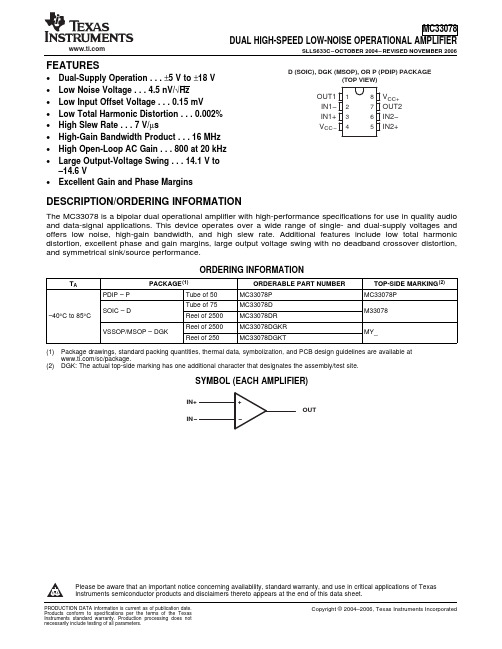
FEATURES12348765OUT1IN1−IN1+V CC −V CC+OUT2IN2−IN2+D (SOIC), DGK (MSOP), OR P (PDIP) PACKAGE(TOP VIEW)DESCRIPTION/ORDERINGINFORMATIONOUT•Dual-Supply Operation ...±5V to ±18V •Low Noise Voltage ...4.5nV/√Hz •Low Input Offset Voltage ...0.15mV•Low Total Harmonic Distortion ...0.002%•High Slew Rate ...7V/µs•High-Gain Bandwidth Product ...16MHz •High Open-Loop AC Gain ...800at 20kHz •Large Output-Voltage Swing ...14.1V to –14.6V•Excellent Gain and Phase MarginsThe MC33078is a bipolar dual operational amplifier with high-performance specifications for use in quality audio and data-signal applications.This device operates over a wide range of single-and dual-supply voltages and offers low noise,high-gain bandwidth,and high slew rate.Additional features include low total harmonic distortion,excellent phase and gain margins,large output voltage swing with no deadband crossover distortion,and symmetrical sink/source performance.ORDERING INFORMATIONT APACKAGE (1)ORDERABLE PART NUMBER TOP-SIDE MARKING (2)PDIP –PTube of 50MC33078P MC33078P Tube of 75MC33078D SOIC –DM33078–40°C to 85°CReel of 2500MC33078DR Reel of 2500MC33078DGKR VSSOP/MSOP –DGKMY_Reel of 250MC33078DGKT(1)Package drawings,standard packing quantities,thermal data,symbolization,and PCB design guidelines are available at /sc/package.(2)DGK:The actual top-side marking has one additional character that designates the assembly/test site.SYMBOL (EACH AMPLIFIER)Please be aware that an important notice concerning availability,standard warranty,and use in critical applications of Texas Instruments semiconductor products and disclaimers thereto appears at the end of this data sheet.PRODUCTION DATA information is current as of publication date.Copyright ©2004–2006,Texas Instruments IncorporatedProducts conform to specifications per the terms of the Texas Instruments standard warranty.Production processing does not necessarily include testing of all parameters.Absolute Maximum Ratings (1)Recommended Operating ConditionsDUAL HIGH-SPEED LOW-NOISE OPERATIONAL AMPLIFIERSLLS633C–OCTOBER 2004–REVISED NOVEMBER 2006over operating free-air temperature range (unless otherwise noted)MINMAX UNIT V CC+Supply voltage (2)18V V CC–Supply voltage (2)–18V V CC+–V CC–Supply voltage36V Input voltage,either input (2)(3)V CC+or V CC–V Input current (4)±10mADuration of output short circuit (5)UnlimitedD package97θJA Package thermal impedance,junction to free air (6)(7)DGK package 172°C/W P package85T J Operating virtual junction temperature 150°C T stg Storage temperature range–65150°C (1)Stresses beyond those listed under Absolute Maximum Ratings may cause permanent damage to the device.These are stress ratings only,and functional operation of the device at these or any other conditions beyond those indicated under Recommended Operating Conditions is not implied.Exposure to absolute-maximum-rated conditions for extended periods may affect device reliability.(2)All voltage values,except differential voltages,are with respect to the midpoint between V CC+and V CC–.(3)The magnitude of the input voltage must never exceed the magnitude of the supply voltage.(4)Excessive input current will flow if a differential input voltage in excess of approximately 0.6V is applied between the inputs,unless some limiting resistance is used.(5)The output may be shorted to ground or either power supply.Temperature and/or supply voltages must be limited to ensure the maximum dissipation rating is not exceeded.(6)Maximum power dissipation is a function of T J (max),θJA ,and T A .The maximum allowable power dissipation at any allowable ambient temperature is P D =(T J (max)–T A )/θJA .Operating at the absolute maximum T J of 150°C can affect reliability.(7)The package thermal impedance is calculated in accordance with JESD 51-7.MINMAX UNIT V CC––5–18Supply voltageV V CC+518T AOperating free-air temperature range–4085°C2Submit Documentation FeedbackElectrical CharacteristicsOperating CharacteristicsV CC–=–15V,V CC+=15V,T A =25°C (unless otherwise noted)PARAMETERTEST CONDITIONSMINTYP MAXUNIT T A =25°C0.152V IO Input offset voltage V O =0,R S =10Ω,V CM =0mV T A =–40°C to 85°C 3Input offset voltage αV IO V O =0,R S =10Ω,V CM =0T A =–40°C to 85°C 2µV/°C temperature coefficient T A =25°C300750I IB Input bias current V O =0,V CM =0nA T A =–40°C to 85°C 800T A =25°C25150I IO Input offset currentV O =0,V CM =0nA T A =–40°C to 85°C175Common-mode input voltage V ICR ∆V IO =5mV,V O =0±13±14V rangeT A =25°C90110Large-signal differential A VDR L ≥2k Ω,V O =±10VdBvoltage amplificationT A =–40°C to 85°C 85V OM+10.7R L =600ΩV OM––11.9V OM+13.213.8V OMMaximum output voltage swing V ID =±1VR L =2k ΩVV OM––13.2–13.7V OM+13.514.1R L =10k ΩV OM––14–14.6CMMR Common-mode rejection ratio V IN =±13V80100dB k SVR (1)Supply-voltage rejection ratio V CC+=5V to 15V,V CC–=–5V to –15V 80105dB Source current 1529I OS Output short-circuit current |V ID |=1V,Output to GND mA Sink current –20–37T A =25°C2.052.5I CC Supply current (per channel)V O =0mA T A =–40°C to 85°C 2.75(1)Measured with V CC ±differentially varied at the same timeV CC–=–15V,V CC+=15V,T A =25°C (unless otherwise noted)PARAMETERTEST CONDITIONSMIN TYP MAXUNIT SR Slew rate at unity gain A VD =1,V IN =–10V to 10V,R L =2k Ω,C L =100pF57V/µs GBW Gain bandwidth product f =100kHz 1016MHz B 1Unity gain frequency Open loop 9MHz C L =0pF –11G m Gain margin R L =2k ΩdB C L =100pF –6C L =0pF 55ΦmPhase margin R L =2k Ωdeg C L =100pF40Amp-to-amp isolation f =20Hz to 20kHz–120dB Power bandwidthV O =27V (PP),R L =2k Ω,THD ≤1%120kHz THD Total harmonic distortion V O =3V rms ,A VD =1,R L =2k Ω,f =20Hz to 20kHz 0.002%z o Open-loop output impedance V O =0,f =9MHz 37Ωr id Differential input resistance V CM =0175k ΩC id Differential input capacitance V CM =012pF V n Equivalent input noise voltage f =1kHz,R S =100Ω 4.5nV/√Hz I nEquivalent input noise currentf =1kHz0.5pA/√Hz3Submit Documentation FeedbackScope x 1= 1.0 M ΩΩNOTE:All capacitors are non-polarized.DUAL HIGH-SPEED LOW-NOISE OPERATIONAL AMPLIFIERSLLS633C–OCTOBER 2004–REVISED NOVEMBER 2006Figure 1.Voltage Noise Test Circuit (0.1Hz to 10Hz)4Submit Documentation FeedbackTYPICAL CHARACTERISTICS10020030040050060056789101112131415161718V CC+/–V CC––Supply Voltage –VI I B –I n p u t B i a s C u r r e n t –nA0100200300400500600-15-10-5051015V CM –Common Mode Voltage –VI I B –I n p u t B i a s C u r r e n t –nA1002003004005006007008009001000-55-35-15525456585105125T A –Temperature –°CI I B –I n p u t B i a s C u r r e n t –nA-2-1.5-1-0.500.511.52-55-35-15525456585105125T A –Temperature –°CV I O –I n p u t O f f s e t V o l t a g e –mVINPUT BIAS CURRENTINPUT BIAS CURRENTvsvsCOMMON-MODE VOLTAGESUPPLY VOLTAGEINPUT BIAS CURRENTINPUT OFFSET VOLTAGEvsvsTEMPERATURETEMPERATURE5Submit Documentation Feedback00.20.40.60.811.21.4-55-255356595125T A –Temperature –°CI n p u t C o m m o n -M o d e V o l t a g e L o w P r o x i m i t y t o V C C ––V-1.4-1.2-1-0.8-0.6-0.4-0.20-55-255356595125T A –Temperature –°CI n p u t C o m m o n -M o d e V o l t a g e H i g h P r o x i m i t y t o V C C +–V01234567891000.511.522.533.544.5R L –Load Resistance–k @O u t p u t S a t u r a t i o n V o l t a g eP r o x i m i t y t o V C C ––VW -10-9-8-7-6-5-4-3-2-1000.511.522.533.544.5R L –Load Resistance –k hO u t p u t S a t u r a t i o n V o l t a g e P r o x i m i t y t o V C C +–VW DUAL HIGH-SPEED LOW-NOISE OPERATIONAL AMPLIFIERSLLS633C–OCTOBER 2004–REVISED NOVEMBER 2006TYPICAL CHARACTERISTICS (continued)INPUT COMMON-MODE VOLTAGEINPUT COMMON-MODE VOLTAGELOW PROXIMITY TO V CC–HIGH PROXIMITY TO V CC+vsvsTEMPERATURETEMPERATUREOUTPUT SATURATION VOLTAGE PROXIMITY TO V CC+OUTPUT SATURATION VOLTAGE PROXIMITY TO V CC–vsvsLOAD RESISTANCE LOAD RESISTANCE6Submit Documentation Feedback10203040506070-55-35-15525456585105125T A –Temperature –°CI O S –O u t p u t S h o r t -C i r c u i t C u r r e n t –m A012345678910-55-35-15525456585105125T A –Temperature –°CI C C –S u p p l y C u r r e n t –m A01020304050607080901001.0E+02 1.0E+03 1.0E+04 1.0E+05 1.0E+06 1.0E+07f –Frequency –HzC M M R –d B1001k 10k 100k 1M 10M 01020304050607080901001101201.0E+02 1.0E+03 1.0E+04 1.0E+05 1.0E+06 1.0E+07f –Frequency –HzP S R R –d B1001k 10k 100k 1M10M TYPICAL CHARACTERISTICS (continued)OUTPUT SHORT-CIRCUIT CURRENTSUPPLY CURRENTvsvsTEMPERATURETEMPERATURECMRR PSSR vsvsFREQUENCYFREQUENCY7Submit Documentation Feedback051015202530-55-35-15525456585105125T A –Temperature –°CG B W –G a i n B a n d w i d t h P r o d u c t –M Hz05101520253056789101112131415161718V CC+/–V CC––Supply Voltage –VG B W –G a i n d B a n d w i d t h P r o d u c t –M H z510152025301.E+011.E+02 1.E+03 1.E+04 1.E+05 1.E+06 1.E+07f –Frequency –HzV O –O u t p u t V o l t a g e –V1001k 10k 100k 1M 10M 10-20-15-10-50510152056789101112131415161718V CC+/–V CC––Supply Voltage –VV O –O u t p u t V o l t a g e –VDUAL HIGH-SPEED LOW-NOISE OPERATIONAL AMPLIFIERSLLS633C–OCTOBER 2004–REVISED NOVEMBER 2006TYPICAL CHARACTERISTICS (continued)GAIN BANDWIDTH PRODUCTGAIN BANDWIDTH PRODUCTvsvsSUPPLY VOLTAGETEMPERATUREOUTPUT VOLTAGEOUTPUT VOLTAGEvsvsSUPPLY VOLTAGEFREQUENCY8Submit Documentation Feedback8085909510010511056789101112131415161718V CC+/–V CC––Supply Voltage –VA V –O p e n -L o o p G a i n –dB80859095100105110115120-55-35-15525456585105125T A –Temperature –°CA V –O p e n -L o o p G a i n –dB1001101201301401501601701801902001.E+01 1.E+02 1.E+031.E+04 1.E+05f –Frequency –HzC r o s s t a l k R e j e c t i o n –d B1k 10k 100k101001.0E+03 1.0E+04 1.0E+05 1.0E+06 1.0E+07f –Frequency –HzZ O –O u t p u t I m p e d a n c e –W1k10k 100k 1M 10MTYPICAL CHARACTERISTICS (continued)OPEN-LOOP GAINOPEN-LOOP GAINvsvsSUPPLY VOLTAGETEMPERATUREOUTPUT IMPEDANCECROSSTALK REJECTIONvsvsFREQUENCYFREQUENCY9Submit Documentation Feedback0.00010.0010.010.111.E+011.E+021.E+031.E+041.E+05f –Frequency –HzT H D –T o t a l H a r m o n i c D i s t o r t i o n –%1k 10k 100k 101000.00010.0010.010.110123456789V O –Output Voltage –V rmsT H D –T o t a l H a r mo n i c D i s t o r t i o n –%234567891056789101112131415161718V CC+/–V CC––Supply Voltage –VS R –S l e w R a t e –V /µs2345678910-55-35-15525456585105125T A –Temperature –°CS R –S l e w R a t e –V /µsDUAL HIGH-SPEED LOW-NOISE OPERATIONAL AMPLIFIERSLLS633C–OCTOBER 2004–REVISED NOVEMBER 2006TYPICAL CHARACTERISTICS (continued)TOTAL HARMONIC DISTORTIONTOTAL HARMONIC DISTORTIONvsvsFREQUENCYOUTPUT VOLTAGESLEW RATESLEW RATEvsvsSUPPLY VOLTAGETEMPERATURE10Submit Documentation Feedbackf –Frequency –HzC out –Output Load Capacitance –pF 0102030405060708090100101001000C out –Output Load Capacitance –pF O v e r s h o o t –%110100100100010000100000f –Frequency –Hz I n p u t V o l t a g e N o i s e 0.1110I n p u t C u r r e n t N o i s e 101k 10k 100k OVERSHOOT INPUT VOLTAGE AND CURRENT NOISE vs vs OUTPUT LOAD CAPACITANCEFREQUENCY11010010001.E+01 1.E+02 1.E+03 1.E+04 1.E+05 1.E+06R S –Source Resistance –èI n p u t R e f e r r e d N o i s e V o l t a g e W 101001k 10k 100k 1M 0246810121416010100100010000100000R SD –Differential Source Resistance –èG a i n M a r g i n –d B 0481216202428323640444852566064P h a s e M a r g i n –d e g W 1k 10k 100k 1000110-22610141822Time –µs -22610141822Time –µs V I –I n p u t V o l t a g e –V MC33078DUAL HIGH-SPEED LOW-NOISE OPERATIONAL AMPLIFIERSLLS633C–OCTOBER 2004–REVISED NOVEMBER 2006TYPICAL INPUT REFERRED NOISE VOLTAGE vs SOURCE RESISTANCELARGE SIGNAL TRANSIENT RESPONSE LARGE SIGNAL TRANSIENT RESPONSE (A V =1)(A V =–1)-0.50.00.5 1.0 1.5Time–µs-500-400-300-200-100100200300400-5-4-3-2-1012345Time–sMC33078 DUAL HIGH-SPEED LOW-NOISE OPERATIONAL AMPLIFIERSLLS633C–OCTOBER2004–REVISED NOVEMBER2006TYPICAL CHARACTERISTICS(continued)SMALL SIGNAL TRANSIENT RESPONSE LOW_FREQUENCY NOISEAPPLICATION INFORMATIONOutput Characteristics250 ns per Division250 ns per Division250 ns per Division0.25V p e r D i v i s i o n 250 ns per Division 0.25V p e r D i v i s i o n250 ns per Division0.25V p e r D i v i s i o n 250 ns per Division0.25V p e r D i v i s i o n5V–5VV OΩMC33078DUAL HIGH-SPEED LOW-NOISE OPERATIONAL AMPLIFIERSLLS633C–OCTOBER 2004–REVISED NOVEMBER 2006All operating characteristics are specified with 100-pF load capacitance.The MC33078can drive higher capacitance loads.However,as the load capacitance increases,the resulting response pole occurs at lower frequencies,causing ringing,peaking,or oscillation.The value of the load capacitance at which oscillation occurs varies from lot to lot.If an application appears to be sensitive to oscillation due to load capacitance,adding a small resistance in series with the load should alleviate the problem (see Figure 2).PULSE RESPONSE PULSE RESPONSE PULSE RESPONSE (R L =600Ω,C L =380pF)(R L =2k Ω,C L =560pF)(R L =10k Ω,C L =590pF)PULSE RESPONSE PULSE RESPONSE PULSE RESPONSE (R O =0Ω,C O =1000pF,R L =2k Ω)(R O =4Ω,C O =1000pF,R L =2k Ω)(R O =35Ω,C O =1000pF,R L =2k Ω)Figure 2.Output CharacteristicsPACKAGING INFORMATIONOrderable Device Status(1)PackageType PackageDrawingPins PackageQtyEco Plan(2)Lead/Ball Finish MSL Peak Temp(3)MC33078D ACTIVE SOIC D875Green(RoHS&no Sb/Br)CU NIPDAU Level-1-260C-UNLIMMC33078DE4ACTIVE SOIC D875Green(RoHS&no Sb/Br)CU NIPDAU Level-1-260C-UNLIMMC33078DG4ACTIVE SOIC D875Green(RoHS&no Sb/Br)CU NIPDAU Level-1-260C-UNLIMMC33078DGKR ACTIVE MSOP DGK82500Green(RoHS&no Sb/Br)CU NIPDAU Level-1-260C-UNLIMMC33078DGKRG4ACTIVE MSOP DGK82500Green(RoHS&no Sb/Br)CU NIPDAU Level-1-260C-UNLIMMC33078DGKT ACTIVE MSOP DGK8250Green(RoHS&no Sb/Br)CU NIPDAU Level-1-260C-UNLIMMC33078DGKTG4ACTIVE MSOP DGK8250Green(RoHS&no Sb/Br)CU NIPDAU Level-1-260C-UNLIMMC33078DR ACTIVE SOIC D82500Green(RoHS&no Sb/Br)CU NIPDAU Level-1-260C-UNLIMMC33078DRE4ACTIVE SOIC D82500Green(RoHS&no Sb/Br)CU NIPDAU Level-1-260C-UNLIMMC33078DRG4ACTIVE SOIC D82500Green(RoHS&no Sb/Br)CU NIPDAU Level-1-260C-UNLIMMC33078P ACTIVE PDIP P850Pb-Free(RoHS)CU NIPDAU N/A for Pkg TypeMC33078PE4ACTIVE PDIP P850Pb-Free(RoHS)CU NIPDAU N/A for Pkg Type(1)The marketing status values are defined as follows:ACTIVE:Product device recommended for new designs.LIFEBUY:TI has announced that the device will be discontinued,and a lifetime-buy period is in effect.NRND:Not recommended for new designs.Device is in production to support existing customers,but TI does not recommend using this part in a new design.PREVIEW:Device has been announced but is not in production.Samples may or may not be available.OBSOLETE:TI has discontinued the production of the device.(2)Eco Plan-The planned eco-friendly classification:Pb-Free(RoHS),Pb-Free(RoHS Exempt),or Green(RoHS&no Sb/Br)-please check /productcontent for the latest availability information and additional product content details.TBD:The Pb-Free/Green conversion plan has not been defined.Pb-Free(RoHS):TI's terms"Lead-Free"or"Pb-Free"mean semiconductor products that are compatible with the current RoHS requirements for all6substances,including the requirement that lead not exceed0.1%by weight in homogeneous materials.Where designed to be soldered at high temperatures,TI Pb-Free products are suitable for use in specified lead-free processes.Pb-Free(RoHS Exempt):This component has a RoHS exemption for either1)lead-based flip-chip solder bumps used between the die and package,or2)lead-based die adhesive used between the die and leadframe.The component is otherwise considered Pb-Free(RoHS compatible)as defined above.Green(RoHS&no Sb/Br):TI defines"Green"to mean Pb-Free(RoHS compatible),and free of Bromine(Br)and Antimony(Sb)based flame retardants(Br or Sb do not exceed0.1%by weight in homogeneous material)(3)MSL,Peak Temp.--The Moisture Sensitivity Level rating according to the JEDEC industry standard classifications,and peak solder temperature.Important Information and Disclaimer:The information provided on this page represents TI's knowledge and belief as of the date that it is provided.TI bases its knowledge and belief on information provided by third parties,and makes no representation or warranty as to the accuracy of such information.Efforts are underway to better integrate information from third parties.TI has taken and continues to take reasonable steps to provide representative and accurate information but may not have conducted destructive testing or chemical analysis on incoming materials and chemicals.TI and TI suppliers consider certain information to be proprietary,and thus CAS numbers and other limited information may not be available for release.In no event shall TI's liability arising out of such information exceed the total purchase price of the TI part(s)at issue in this document sold by TI to Customer on an annual basis.OTHER QUALIFIED VERSIONS OF MC33078:•Enhanced Product:MC33078-EPNOTE:Qualified Version Definitions:•Enhanced Product-Supports Defense,Aerospace and Medical ApplicationsTAPE AND REEL INFORMATION*All dimensions are nominal Device Package Type Package DrawingPinsSPQ Reel Diameter (mm)Reel Width W1(mm)A0(mm)B0(mm)K0(mm)P1(mm)W (mm)Pin1Quadrant MC33078DGKR MSOPDGK 82500330.012.4 5.3 3.3 1.38.012.0Q1MC33078DGKT MSOPDGK 8250180.012.4 5.3 3.3 1.38.012.0Q1MC33078DR SOIC D 82500330.012.4 6.4 5.2 2.18.012.0Q1*All dimensions are nominalDevice Package Type Package Drawing Pins SPQ Length(mm)Width(mm)Height(mm) MC33078DGKR MSOP DGK82500346.0346.035.0 MC33078DGKT MSOP DGK8250220.0205.050.0MC33078DR SOIC D8*******.0346.029.0IMPORTANT NOTICETexas Instruments Incorporated and its subsidiaries(TI)reserve the right to make corrections,modifications,enhancements,improvements, and other changes to its products and services at any time and to discontinue any product or service without notice.Customers should obtain the latest relevant information before placing orders and should verify that such information is current and complete.All products are sold subject to TI’s terms and conditions of sale supplied at the time of order acknowledgment.TI warrants performance of its hardware products to the specifications applicable at the time of sale in accordance with TI’s standard warranty.Testing and other quality control techniques are used to the extent TI deems necessary to support this warranty.Except where mandated by government requirements,testing of all parameters of each product is not necessarily performed.TI assumes no liability for applications assistance or customer product design.Customers are responsible for their products and applications using TI components.To minimize the risks associated with customer products and applications,customers should provide adequate design and operating safeguards.TI does not warrant or represent that any license,either express or implied,is granted under any TI patent right,copyright,mask work right, or other TI intellectual property right relating to any combination,machine,or process in which TI products or services are rmation published by TI regarding third-party products or services does not constitute a license from TI to use such products or services or a warranty or endorsement e of such information may require a license from a third party under the patents or other intellectual property of the third party,or a license from TI under the patents or other intellectual property of TI.Reproduction of TI information in TI data books or data sheets is permissible only if reproduction is without alteration and is accompanied by all associated warranties,conditions,limitations,and notices.Reproduction of this information with alteration is an unfair and deceptive business practice.TI is not responsible or liable for such altered rmation of third parties may be subject to additional restrictions.Resale of TI products or services with statements different from or beyond the parameters stated by TI for that product or service voids all express and any implied warranties for the associated TI product or service and is an unfair and deceptive business practice.TI is not responsible or liable for any such statements.TI products are not authorized for use in safety-critical applications(such as life support)where a failure of the TI product would reasonably be expected to cause severe personal injury or death,unless officers of the parties have executed an agreement specifically governing such use.Buyers represent that they have all necessary expertise in the safety and regulatory ramifications of their applications,and acknowledge and agree that they are solely responsible for all legal,regulatory and safety-related requirements concerning their products and any use of TI products in such safety-critical applications,notwithstanding any applications-related information or support that may be provided by TI.Further,Buyers must fully indemnify TI and its representatives against any damages arising out of the use of TI products in such safety-critical applications.TI products are neither designed nor intended for use in military/aerospace applications or environments unless the TI products are specifically designated by TI as military-grade or"enhanced plastic."Only products designated by TI as military-grade meet military specifications.Buyers acknowledge and agree that any such use of TI products which TI has not designated as military-grade is solely at the Buyer's risk,and that they are solely responsible for compliance with all legal and regulatory requirements in connection with such use. TI products are neither designed nor intended for use in automotive applications or environments unless the specific TI products are designated by TI as compliant with ISO/TS16949requirements.Buyers acknowledge and agree that,if they use any non-designated products in automotive applications,TI will not be responsible for any failure to meet such requirements.Following are URLs where you can obtain information on other Texas Instruments products and application solutions:Products ApplicationsAudio /audio Communications and Telecom /communicationsAmplifiers Computers and Peripherals /computersData Converters Consumer Electronics /consumer-appsDLP®Products Energy and Lighting /energyDSP Industrial /industrialClocks and Timers /clocks Medical /medicalInterface Security /securityLogic Space,Avionics and Defense /space-avionics-defense Power Mgmt Transportation and /automotiveAutomotiveMicrocontrollers Video and Imaging /videoRFID Wireless /wireless-appsRF/IF and ZigBee®Solutions /lprfTI E2E Community Home Page Mailing Address:Texas Instruments,Post Office Box655303,Dallas,Texas75265Copyright©2011,Texas Instruments Incorporated。
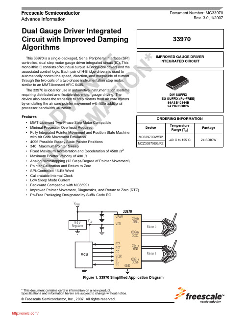
Document Number: MC33970Rev. 3.0, 1/2007Freescale Semiconductor Advance Information* This document contains certain information on a new product.Specifications and information herein are subject to change without notice.© Freescale Semiconductor, Inc., 2007. All rights reserved.Dual Gauge Driver Integrated Circuit with Improved Damping••••••••••••Low Sleep Mode Current•Backward Compatible with MC33991•Improved Pointer Movement, Diagnostics, and Return to Zero (RTZ) •Pb-Free Packaging Designated by Suffix Code EGFigure 1. 33970 Simplified Application Diagram33970Analog Integrated Circuit Device Data33970INTERNAL BLOCK DIAGRAMINTERNAL BLOCK DIAGRAMFigure 2. 33970 Simplified Internal Block DiagramH-BRIDGE COS0+INTERNAL VPWRVDDSIN0COS0COS0-SIN0+SIN0-COS1+COS1-COS1REGULATORLOGICSPIILIMOVERTEMPERATUREAND CONTROLSIN1OSCILLATORDETECTUNDER -ANDOVERVOLTAGE DETECTCS SCLK SO SIRSTRTZSIN1+SIN1-GND (8)MULTIPLEXERSIGMA-DELTAADCAGNDSTATE MACHINEVDDAnalog Integrated Circuit Device Data 33970PIN CONNECTIONSPIN CONNECTIONSFigure 3. 33970 Pin ConnectionsTable 1. 33970 Pin DefinitionsA functional description of each pin can be found in the Functional Pin Description section beginning on page 10.Pin NumberPin Name Pin FunctionFormal Name Definition1234COS0+COS0−SIN0+SIN0−OutputH-Bridge Outputs 0Each pin is the output pin of a half bridge, designed to source or sink current.5 – 8,17– 20GND Ground Ground These pins serve as the ground for the source of the low-side output transistors as well as the logic portion of the device.9CS Input Chip Select This pin is connected to a chip select output of a LSI IC.10SCLK Input Serial Clock This pin is connected to the SCLK pin of the master device and acts as a bit clock for the SPI port.11SO Output Serial Output This pin is connected to the SPI Serial Data Input pin of the master device, or to the SI pin of the next device in a daisy chain.12SI Input Serial Input This pin is connected to the SPI Serial Data Output pin of the master device from which it receives output command data.13RTZ Output Multiplexed OutputThis is a multiplexed output pin, for the non-driven coil, during a Return to Zero (RTZ) event.14VDD Input Voltage This SPI and logic power supply input will work with 5.0 V supplies. 15RST Input Reset This input has an internal active pull-up. 16VPWR Input Battery Voltage Power supply.21222324SIN1−SIN1+COS1−COS1+OutputH-Bridge Outputs 1Each of these pins are the output pin of a half bridge, designed to source or sink current.COS0+COS0-SIN0+SIN0-GND GND GND CS SCLK SO SI123456789101112242322212019181716151413COS1+COS1-SIN1+SIN1-GND GND GND VPWR RST VDD RTZGND GNDAnalog Integrated Circuit Device Data33970ELECTRICAL CHARACTERISTICS MAXIMUM RATINGSELECTRICAL CHARACTERISTICSMAXIMUM RATINGSTable 2. Maximum RatingsAll voltages are with respect to ground unless otherwise noted. Exceeding these ratings may cause a malfunction or permanent damage to the device.RatingsSymbolValueUnitELECTRICAL RATINGS Power Supply Voltage Steady State V PWR(SUS)-0.3 to 41VInput Pin Voltage (1)V IN -0.3 to 7.0V SIN +/- COS +/- Continuous Per Output Current (2)I OUTMAX 40mA ESD Voltage (3)Human Body Model Machine Model V ESD1V ESD2±2000 ±200V THERMAL RATINGS Storage TemperatureT STG -55 to 150°C Operating Junction Temperature T J-40 to 150°C Thermal Resistance Junction to Ambient Junction to Lead R θJA R θJL6020°C/WTHERMAL RESISTANCEPeak Package Reflow Temperature During Reflow (4), (5)T PPRTNote 5°CNotes1.Exceeding voltage limits on Input pins may cause permanent damage to the device.2.Output continuous output rating so long as maximum junction temperature is not exceeded. Operation at 125°C ambient temperaturewill require maximum output current computation using package thermal resistances.3.ESD1 testing is performed in accordance with the Human Body Model (C ZAP = 100 pF, R ZAP = 1500 Ω), ESD2 testing is performed inaccordance with the Machine Model (C ZAP = 200 pF, R ZAP = 0 Ω).4.Pin soldering temperature limit is for 10 seconds maximum duration. Not designed for immersion soldering. Exceeding these limits may cause malfunction or permanent damage to the device.5.Freescale’s Package Reflow capability meets Pb-free requirements for JEDEC standard J-STD-020C. For Peak Package Reflow Temperature and Moisture Sensitivity Levels (MSL),Go to , search by part number [e.g. remove prefixes/suffixes and enter the core ID to view all orderable parts. (i.e. MC33xxxD enter 33xxx), and review parametrics.Analog Integrated Circuit Device Data 33970ELECTRICAL CHARACTERISTICSSTATIC ELECTRICAL CHARACTERISTICSSTATIC ELECTRICAL CHARACTERISTICSTable 3. Static Electrical CharacteristicsCharacteristics noted under conditions 4.75 V < V DD < 5.25 V, -40°C < T A < 125°C, GND = 0 V unless otherwise noted. Typical values noted reflect the approximate parameter means at T A = 25°C under nominal conditions unless otherwise noted.CharacteristicSymbol Min Typ Max UnitPOWER INPUT Supply Voltage Range Fully Operational Limited Operational (6),(7)V PWR6.54.0––2626VVPWR Supply CurrentGauge 1 and 2 Outputs ON, No Output Loads I PWR(ON)–4.06.0mAVPWR Supply Current (All Outputs Disabled)Reset = Logic [0], V DD = 5.0 V Reset = Logic [0], V DD = 0 V I PWSLP1I PWRSLP2––42156025µAOvervoltage Detection Level (8)V PWROV 263238V Undervoltage Detection Level (9)V PWRUV 5.0 5.6 6.2V Logic Supply Voltage Range (5.0 V Nominal Supply)V DD 4.5 5.0 5.5V Under VDD Logic Reset V DDUV––4.5VVDD Supply Current Sleep: Reset Logic [0]Outputs Enabled I DD(OFF)I DD(ON)––401.0651.8µA mAPOWER OUTPUTSMicrostep Output (Measured Across Coil Outputs) SIN0,1, ± (COS0,1, ±) (refer to Table 1)R OUT = 200 ΩSteps 6, 18 (0, 12)Steps 5, 7, 17, 19 (1, 11, 13, 23)Steps 4, 8, 16, 20 (2, 10, 14, 22)Steps 3, 9, 15, 21 (3, 9, 15, 21)Steps 2, 10, 14, 22 (4, 8,16, 20)Steps 1, 11, 13, 23 (5, 7, 17, 19)Steps 0, 12 (6, 18)V ST6V ST5V ST4V ST3V ST2V ST1V ST0 4.820.94 V ST60.84 V ST60.68 V ST60.47 V ST60.23 V ST6-0.15.30.97 V ST60.87 V ST60.71 V ST60.50 V ST60.26 V ST60.06.01.0 V ST60.96 V ST60.8 V ST60.57 V ST60.31 V ST60.1VFull Step Active Output (Measured Across Coil Outputs) SIN0, 1, ± (COS0, 1, ±) (see Figure 9, page 23)Steps 1, 3 (0, 2)V FS4.95.36.0V Microstep, Full Step Output (Measured from Coil Low Side to Ground)SIN0, 1, ± (COS0, 1, ±), I OUT = 30 mAV LS0.00.10.3VNotes6.Outputs and logic remain active; however, the larger coil voltage levels may be clipped. The reduction in drive voltage may result in aloss of position control.7.The logic will reset at some level below the specified Limited Operational minimum. 8.Outputs will disable and must be re-enabled via the PECCR command.9.Outputs remain active; however, the reduction in drive voltage may result in a loss of position control.Analog Integrated Circuit Device Data33970ELECTRICAL CHARACTERISTICSSTATIC ELECTRICAL CHARACTERISTICSPOWER OUTPUTS (continued)Output Flyback Clamp (10)V FB –V ST6 + 0.5V ST6 + 1.0V Output Current Limit (Output = VST6)I LIM 40100170mA Overtemperature Shutdown (10)OT SD 155–180°C Overtemperature Hysteresis (10)OT HYST8.0–16°CCONTROL I/OInput Logic High Voltage (11)V IH 2.0––V Input Logic Low Voltage (11)V IL ––0.8V Input Logic Voltage Hysteresis (10)V IN(HYST)–100–mV Input Logic Pull Down Current (SI, SCLK)I DWN 3.0–20µA Input Logic Pull-Up Current (CS , RST )I UP 5.0–20µA SO High-State Output Voltage (I OH = 1.0 mA)V SOH 0.8 V DD––V SO Low-State Output Voltage (I OL = -1.6 mA)V SOL –0.20.4V SO Tri-State Leakage Current (CS ≥ 3.5 V)I SOLK -5.00 5.0µA Input Capacitance (12)C IN – 4.012pF SO Tri-State Capacitance (12)C SO––20pFANALOG TO DIGITAL CONVERTER (RTZ ACCUMULATOR COUNT)ADC Gain (10), (13)G ADC100188270Counts/V/msNotes10.This parameter is guaranteed by design; however, it is not production tested.11.V DD = 5.0 V.12.Capacitance not measured. This parameter is guaranteed by design; however, it is not production tested.13.Reference Figure 8, RTZ Accumulator (Typical)Table 3. Static Electrical Characteristics (continued)Characteristics noted under conditions 4.75 V < V DD < 5.25 V, -40°C < T A < 125°C, GND = 0 V unless otherwise noted. Typical values noted reflect the approximate parameter means at T A = 25°C under nominal conditions unless otherwise noted.CharacteristicSymbolMinTypMaxUnitAnalog Integrated Circuit Device Data 33970ELECTRICAL CHARACTERISTICSDYNAMIC ELECTRICAL CHARACTERISTICSDYNAMIC ELECTRICAL CHARACTERISTICSTable 4. Dynamic Electrical CharacteristicsCharacteristics noted under conditions 4.75 V < V DD < 5.25 V, -40°C < T A < 125°C, GND = 0 V unless otherwise noted. Typical values noted reflect the approximate parameter means at T A = 25°C under nominal conditions unless otherwise noted.CharacteristicSymbolMinTypMaxUnitPOWER OUTPUT AND CLOCK TIMINGSSIN, COS Output Turn ON Delay Time (Time from Rising CS Enabling Outputs to Steady State Coil Voltages and Currents) (14)t DLY (ON)––1.0msSIN, COS Output Turn OFF Delay Time (Time from Rising CS Disables Outputs to Steady State Coil Voltages and Currents) (14)t DLY (OFF)–– 1.0msUncalibrated Oscillator Cycle Time t CLU 0.65 1.01.7µs Calibrated Oscillator Cycle TimeCal Pulse = 8.0 µs, PECCR D4 = Logic [0]Cal pulse = 8.0 µs, PECCR D4 = Logic [1]t CLC1.00.9 1.11.0 1.21.1µsMaximum Pointer Speed (15)V MAX ––400°/s Maximum Pointer Acceleration (15) A MAX ––4500°/s 2SPI INTERFACE TIMING (16)Recommended Frequency of SPI Operationf SPI – 1.0 3.0MHz Falling Edge of CS to Rising Edge of SCLK (Required Setup Time) (17)t LEAD –50167ns Falling Edge of SCLK to Rising Edge of CS (Required Setup Time) (17)t LAG –50167ns SI to Falling Edge of SCLK (Required Setup Time) (17)t S ISU –2583ns Required High State Duration of SCLK (Required Setup Time) (17)t WSCLKH ––167ns Required Low State Duration of SCLK (Required Setup Time) (17)t WSCLKL ––167ns Falling Edge of SCLK to SI (Required Hold Time) (17)t SI (HOLD)–2583ns SO Rise Time C L = 200 pF t R SO–2550nsSO Fall Time C L = 200 pFt F SO–2550nsSI, CS , SCLK, Incoming Signal Rise Time (18)t RSI ––50ns SI, CS , SCLK, Incoming Signal Fall Time (18)t F SI ––50ns Falling Edge of RST to Rising Edge of RST (Required Setup Time) (17)t W RST –– 3.0µs Rising Edge of CS to Falling Edge of CS (Required Setup Time) (17), (19) t CS –– 5.0µs Rising Edge of RST to Falling Edge of CS (Required Setup Time) (17)t EN ––5.0µsNotes14.Maximum specified time for the 33970 is the minimum guaranteed time needed from the microcontroller.15.The minimum and maximum value will vary proportionally to the internal clock tolerance. These numbers are based on an ideallycalibrated clock frequency of 1.0 MHz. These are not 100 percent tested.16.The device shall meet all SPI interface timing requirements specified in the SPI Interface Timing section of this table, over the temperaturerange specified. Digital interface timing is based on a symmetrical 50 percent duty cycle SCLK Clock Period of 333 ns. The device shall be fully functional for slower clock speeds. See Figure 4 and 5.17.The maximum setup time specified for the 33970 is the minimum time needed from the microcontroller to guarantee correct operation.18.Rise and Fall time of incoming SI, CS, and SCLK signals suggested for design consideration to prevent the occurrence of double pulsing.19.The value is for a 1.0 MHz calibrated internal clock. The value will change proportionally as the internal clock frequency changesAnalog Integrated Circuit Device Data33970ELECTRICAL CHARACTERISTICSDYNAMIC ELECTRICAL CHARACTERISTICSTime from Falling Edge of CS to SO Low Impedance (20)t SO(EN)––145ns Time from Rising Edge of CS to SO High Impedance (21)t SO(DIS)–1.34.0µs Time from Rising Edge of SCLK to SO Data Valid (22)0.2 V DD ≤ SO ≥ 0.8 V DD , C L = 200 pFt VALID–65105nsNotes20.Time required for output status data to be terminated at SO. 1.0 k Ω load on SO21.Time required for output status data to be available for use at SO. 1.0 k Ω load on SO.22.Time required to obtain valid data out from SO following the rise of SCLK.Table 4. Dynamic Electrical CharacteristicsCharacteristics noted under conditions 4.75 V < V DD < 5.25 V, -40°C < T A < 125°C, GND = 0 V unless otherwise noted. Typical values noted reflect the approximate parameter means at T A = 25°C under nominal conditions unless otherwise noted.CharacteristicSymbol Min Typ Max UnitAnalog Integrated Circuit Device Data 33970ELECTRICAL CHARACTERISTICSTIMING DIAGRAMSTIMING DIAGRAMSFigure 4. Input Timing Switching CharacteristicsFigure 5. Valid Data Delay Time and Valid Time WaveformsRSTCSSISCLKV INV ILV IH V ILV IH V ILV IHV ILDon’t CareValidValidDon’t CareDon’t Care0.2 V DD0.2 V DD 0.2 V DD0.7 V DD0.7 V DD0.7 V DD 0.7 V DDt ENt WRSTt CSt LAGt RSIt LEAD t LEADt WSCLKht WSCLKlt FSIt SI(HOLD)SCLKSOSOLow-to-HighHigh-to-Low3.5 V0.2 V DD0.7 V DD0.2 V DD1.0 VV OHV OLV OH V OLV OH V OLt FSIt RSI0.7 V DD50%t SO(EN)t RSOt FSOt SO(DIS)t VALIDAnalog Integrated Circuit Device Data33970FUNCTIONAL DESCRIPTION INTRODUCTIONFUNCTIONAL DESCRIPTIONINTRODUCTIONThis 33970 is a single-packaged, Serial Peripheral Interface (SPI) controlled, dual step motor gauge driverintegrated circuit (IC). This monolithic IC consists of four dual output H-Bridge coil drivers and the associated control logic. Each pair of H-Bridge drivers is used to automatically control the speed, direction, and magnitude of current through the two coils of a two-phase instrumentation step motor, similar to an MMT-licensed AFIC 6405.The 33970 is ideal for use in automotive instrumentation systems requiring distributed and flexible step motor gauge driving. The device also eases the transition to step motors from air core motors by emulating the air core pointer movement with little additional processor bandwidth utilization.FUNCTIONAL PIN DESCRIPTIONH-Bridge Outputs 0 (COS0+, COS0-, SIN0+, SIN0-)Each pin is the output pin of a half bridge, designed to source or sink current. The H-Bridge pins linearly drive the sine and cosine coils of two separate step motors to provide four-quadrant operation.GROUND (GND)These pins serve as the ground for the source of the low-side output transistors as well as the logic portion of the device. They also help dissipate heat from the device.CHIP SELECT (CS)The CS pin enables communication with the master device. When this pin is in a logic [0] state, the 33970 is capable of transferring information to, and receivinginformation from, the master. The 33970 latches data in from the Input Shift registers to the addressed registers on the rising edge of CS when CS is logic [0]. When CS is logic high, signals at the SCLK and SI pins are ignored and the SO pin is tri-stated (high impedance). CS will only be transitioned from a logic [1] state to a logic [0] state when SCLK is a logic [0]. CS has an internal pull-up (l UP ) connected to the pin, as specified in the section of the Static Electrical Characteristics table entitled CONTROL I/O , which is found on page 6.SERIAL CLOCK (SCLK)SCLK clocks the Internal Shift registers of the 33970 device. The Serial Input (SI) pin accepts data into the Input Shift register on the falling edge of the SCLK signal, while the Serial Output pin (SO) shifts data information out of the SO Line Driver on the rising edge of the SCLK signal. It isimportant that the SCLK pin be in a logic [0] state whenever the CS makes any transition. SCLK has an internal pull down (l DWN ), as specified in the section of the Static Electrical Characteristics table entitled CONTROL I/O , which is found on page 6. When CS is logic [1], signals at the SCLK and SI pins are ignored and SO is tri-stated (high impedance). Refer to the data transfer timing diagrams in Figure 6 and Figure 7 on page 12.SERIAL OUTPUT (SO)The SO data pin is a tri-stateable output from the Shift register. The Status register bits are the first 16 bits shifted out. Those bits are followed by the message bits clocked in FIFO, when the device is in a daisy chain connection or being sent words that are multiples of 16 bits. Data is shifted on the rising edge of the SCLK signal. The SO pin will remain in a high impedance state until the CS pin is put into a logic low state.SERIAL INPUT (SI)The SI pin is the input of the Serial Peripheral Interface (SPI). Serial Input (SI) information is read on the falling edge of SCLK. A 16-bit stream of serial data is required on the SI pin, beginning with the most significant bit (MSB). Messages that are not multiples of 16 bits (e.g., daisy chained device messages) are ignored. After transmitting a 16-bit word, the CS pin must be de-asserted (logic [1]) before transmitting a new word. SI information is ignored when CS state.Multiplexed Output (RTZ)This is a multiplexed output pin, for the non-driven coil, during a Return to Zero (RTZ) event.Voltage (VDD)This SPI and logic power supply input will work with 5.0 V supplies.RESET (RST)If the master decides to reset the device, or place it into a sleep state, the RST pin is driven to a logic [0]. A logic [0] on the RST pin will force all internal logic to the known default state. This input has an internal active pull-up.BATTERY VOLTAGE (VPWR)Power supply.分销商库存信息: FREESCALEMC33970DWR2。

音频运放评测音频运放评测1、皇冠金苹果、MA系列等用的是MC33079四运放,而LAB、变色龙、哈里森等用的是5532、5534运放,BGW150前级放大采用NE5534AN、QUAD-406电压放大采用LM318,雅马哈高级调音台(价格上万的)采用NJM4558D或NJM4558DD或者NJM072D,飞利浦大部分音响设备采用LM833或者LM837(四运放);2、德国坦克有两款声卡采用NJM4580贴片和飞利浦(TI)NE5532,以及NEC的2SB772(P)和2SD882(P)驱动;3、用OP37的机器几乎没有,用所谓高级运放甚至陶封、金封运放如AD712、AD812、AD797、OPA2604、NE5535、HA5112、CA3240等等在成品机中几乎见不到;4、在电路搭配中,决定音色最大的位置不是运放,而是输出阻抗匹配电阻和负反馈回路形式;5、国产山寨宇音PK-1耳机,可以通过换耳壳(PK-1换PK-2耳壳),pk-1外壳开第二个孔,加吸音棉、换等长银线(特氟龙镀银线)、换插头(原始山寨pk-1的插头太差了,经常接触不良)、校正相位和配对直流电阻值、用酒精去掉振膜上那一圈红漆(这个最好不要做,很容易玩死山寨pk-1)、煲耳机300小时来提高山寨PK-1的音质,而且提高比较显著,但不要指望能秒杀森海塞尔MX760。
6、±5V低压供电中,想要省电而且音质好,可采用LM833、MC33078或者NJM45XX系列运放,这几种运放在低压供电下失真比较低,且性能稳定,特别是NJM4556AD,低压性能、噪声水平、驱动能力和稳定性都十分出色;±15V高压供电,要求音质比较好且失真比较小的,可以采用TL072类型(±18V供电)、NE5532/5534(±15V供电)、OPA2604以及OPA2114/NJM2114(±12V供电),需要根据电路供电电源的特征更换运放,不宜随意更换。
MC33077Low Noise Dual Operational AmplifierThe MC33077 is a precision high quality, high frequency, low noise monolithic dual operational amplifier employing innovative bipolar design techniques. Precision matching coupled with a unique analog resistor trim technique is used to obtain low input offset voltages.Dual−doublet frequency compensation techniques are used to enhance the gain bandwidth product of the amplifier. In addition, the MC33077offers low input noise voltage, low temperature coefficient of input offset voltage, high slew rate, high AC and DC open loop voltage gain and low supply current drain. The all NPN transistor output stage exhibits no deadband cross−over distortion, large output voltage swing, excellent phase and gain margins, low open loop output impedance and symmetrical source and sink AC frequency performance.The MC33077 is available in plastic DIP and SOIC−8 packages (P and D suffixes).Features•Low V oltage Noise: 4.4 nV/Hz Ǹ@ 1.0 kHz •Low Input Offset V oltage: 0.2 mV•Low TC of Input Offset V oltage: 2.0 m V/°C•High Gain Bandwidth Product: 37 MHz @ 100 kHz •High AC V oltage Gain: 370 @ 100 kHz1850 @ 20 kHz•Unity Gain Stable: with Capacitance Loads to 500 pF •High Slew Rate: 11 V/m s•Low Total Harmonic Distortion: 0.007%•Large Output V oltage Swing: +14 V to −14.7 V •High DC Open Loop V oltage Gain: 400 k (112 dB)•High Common Mode Rejection: 107 dB •Low Power Supply Drain Current: 3.5 mA •Dual Supply Operation: ±2.5 V to ±18 V •Pb−Free Package is AvailableDevice Package Shipping †ORDERING INFORMATIONMC33077D SOIC−898 Units/Rail MC33077DR2SOIC−82500 Tape & Reel PDIP−8P SUFFIX CASE 62618SOIC−8D SUFFIX CASE 75118MARKING DIAGRAMS1818A = Assembly Location WL, L = Wafer Lot YY , Y = YearWW, W= Work WeekMC33077PPDIP−850 Units/RailPIN CONNECTIONS42V EE 135678V CC Output 2Inputs 2Inputs 1(Dual, Top View)−+1−+2Output 133077ALYWMC33077P AWL YYWWMC33077DR2G SOIC−8(Pb−Free)2500 Tape & Reel †For information on tape and reel specifications,including part orientation and tape sizes, please refer to our T ape and Reel Packaging Specifications Brochure, BRD8011/D.Figure 1. Representative Schematic Diagram (Each Amplifier)MAXIMUM RATINGSMaximum ratings applied to the device are individual stress limit values (not normal operating conditions) and are not valid simultaneously. If stress limits are exceeded device functional operation is not implied, damage may occur and reliability may be affected. Functi onal operation should be restricted to the Recommended Operating Conditions.1.Either or both input voltages should not exceed V CC or V EE (See Applications Information).2.Power dissipation must be considered to ensure maximum junction temperature (T J) is not exceeded (See power dissipation performancecharacteristic, Figure 2).3.Measured with V CC and V EE simultaneously varied.P D (M A X ), M A X I M U M P O W E R D I S S I P A T I O N (m W )Figure 2. Maximum Power Dissipationversus Temperature Figure 3. Input Bias Current versus Supply VoltageT A , AMBIENT TEMPERATURE (°C)V CC , |V EE |, SUPPLY VOLTAGE (V), I N P U T B I A S C U R R E N T (n A )I I B 24002000160012008004008006004002000 2.5 5.07.51012.51517.520Figure 4. Input Bias Currentversus TemperatureFigure 5. Input Offset Voltageversus TemperatureFigure 6. Input Bias Current versusCommon Mode Voltage Figure 7. Input Common Mode Voltage Rangeversus TemperatureFigure 8. Output Saturation Voltage versusLoad Resistance to Ground Figure 9. Output Short Circuit Currentversus TemperatureT A , AMBIENT TEMPERATURE (°C), I N P U T B I A S C U R R E N T (n A )I I B V , I N P U T O F F S E T V O L T A G E (m V )I O T A , AMBIENT TEMPERATURE (°C)V CM , COMMON MODE VOLTAGE (V), I N P U T B I A S C U R R E N T (n A )I IB T A , AMBIENT TEMPERATURE (°C)V I C R , I N P U T C O M M O N M O D E V O T A G E R A N G E (V )R L , LOAD RESISTANCE TO GROUND (k W )V , O U T P U T S A T U R A T I O N V O L T A G E (V )s a tT A , AMBIENT TEMPERATURE (°C)|I |, O U T P U T S H O R T C I R C U I T C U R R E N T (m A )S C1.00.5−0.5−1.06005004003002001000V CC 0.0V CC V CC V CC V EE +1.5V EE +1.0V EE +0.5V EE +0.0V CC V CC V CC V EE V EE V EE 5040302010−55−25025*******125−55−25255075100125Figure 12. Power Supply Rejectionversus Frequency Figure 13. Gain Bandwidth Productversus Supply VoltageFigure 14. Gain Bandwidth Productversus Temperature Figure 15. Maximum Output Voltageversus Supply VoltageI , S U P P L Y C U R R E N T (m A )C Cf, FREQUENCY (Hz)P S R , P O W E R S U P P L Y R E J E C T I O N (d B )V CC , |V EE |, SUPPLY VOLTAGE (V)T A , AMBIENT TEMPERATURE (°C)G B W , G A I N B A N D W I D T H P R O D U C T (M H z )V CC , |V EE |, SUPPLY VOLTAGE (V)V O ,O U T P U T V O L T A G E (V )p 5.0504642383430262015105.0V O ,O U T P U T V O L T A G E (V )p p Figure 16. Output Voltageversus Frequency Figure 17. Open Loop Voltage Gainversus Supply VoltageFigure 20. Channel Separationversus Frequency Figure 21. Total Harmonic Distortionversus Frequencyf, FREQUENCY (Hz)V CC , |V EE |, SUPPLY VOLTAGE (V)O P E N L O O P V O L T A G E G A I N (X 1000 V /V )A V O L ,O P E N L O O P V O L T A G E G A I N (X 1000 V /V )A V O L ,f, FREQUENCY (Hz)C S , C H A N N E L S E P A R A T I O N (d B )f, FREQUENCY (Hz)30252015100110101001.0 k10 k100 kFigure 22. Total Harmonic Distortionversus Frequency Figure 23. Total Harmonic Distortionversus Output VoltageFigure 24. Slew Rate versus Supply Voltage Figure 25. Slew Rate versus TemperatureFigure 26. Voltage Gain and Phaseversus FrequencyFigure 27. Open Loop Gain Margin and Phase Margin versus Output Load CapacitanceT H D ,T O T A L H A R M O N I C D I S T O R T I O N (%)f, FREQUENCY (Hz)V O , OUTPUT VOLTAGE (V pp )T H D , T O T A L H A R M O N I C D I S T O R T I O N (%)V CC , |V EE |, SUPPLY VOLTAGE (V)S R , S L E W R A T E (V / s )µS R , S L E W R A T E (V / s )µT A , AMBIENT TEMPERATURE (°C)f, FREQUENCY (Hz)φ, E X C E S S P H A S E (D E G R E E S )O P E N −L O O P V O L T A G E G A I N (d B )A V O L ,A , O P E N L O O P G A I N M A R G I N (dB )m 0102030405060φ, P H A S E M A R G I N (D E G R E E S )m 70C L , OUTPUT LOAD CAPACITANCE (pF)1.00.140302010014060201412108.06.04.02.010100 1.0 k10 k 100 k 1.0 M 10 M100 M1.0101001000Figure 28. Phase Margin versusOutput VoltageFigure 29. Overshoot versusOutput Load CapacitanceFigure 30. Input Referred Noise Voltageand Current versus FrequencyFigure 31. Total Input Referred Noise Voltageversus Source ResistantFigure 32. Phase Margin and Gain Marginversus Differential Source ResistanceFigure 33. Inverting Amplifier Slew Rate V O, OUTPUT VOLTAGE (V)φ,PHASEMARGIN(DEGREES)mC L, OUTPUT LOAD CAPACITANCE (pF)os,OVERSHOOT(%)f, FREQUENCY (Hz)e,INPUTREFERREDNOISEVOLTAGE()n105.03.02.01.00.50.30.20.1i,INPUTREFERREDNOISECURRENT(pA)nnV/Hz√V,TOTALREFERREDNOISEVOLTAGE()nR S, SOURCE RESISTANCE (W)nV/Hz√10203040506070φm,PHASEMARGIN(DEGREES)R T, DIFFERENTIAL SOURCE RESISTANCE (W)A,GAINMARGIN(dB)mV,OUTPUTVOLTAGE(5.V/DIV)Ot, TIME (2.0 m s/DIV)V70605040302010806040100503020105.03.02.01.01000100101.01412108.06.04.02.01.010100 1.0 k10 kV CC = +15 VV EE = −15 VA V = −1.0R L = 2.0 k WC L = 100 pFT A = 25°CFigure 34. Non−inverting Amplifier Slew Rate Figure 35. Non−inverting Amplifier OvershootFigure 36. Low Frequency Noise Voltageversus TimeV , O U T P U T V O L T A G E (5.0 V /D I V )O t, TIME (2.0 m s/DIV)t, TIME (200 ns/DIV)e , I N P U T N O I S E V O L T A G E (100n V /D I V )n t, TIME (1.0 sec/DIV)V , O U T P U T V O L T A G E (5.0 V /D I V )O V CC = +15 V V EE = −15 V A V = +1.0R L = 2.0 k W T A = 25°CC L = 0 pFC L = 100 pFV CC = +15 VV EE = −15 VBW = 0.1 Hz to 10 Hz T A = 25°CSee Noise Circuit (Figure 36)V CC = +15 VV EE = −15 V A V = +1.0R L = 2.0 k W C L = 100 pF T A = 25°CAPPLICATIONS INFORMATIONThe MC33077 is designed primarily for its low noise, low offset voltage, high gain bandwidth product and large output swing characteristics. Its outstanding high frequency gain/phase performance make it a very attractive amplifier for high quality preamps, instrumentation amps, active filters and other applications requiring precision quality characteristics. The MC33077 utilizes high frequency lateral PNP input transistors in a low noise bipolar differential stage driving a compensated Miller integration amplifier. Dual−doublet frequency compensation techniques are used to enhance the gain bandwidth product. The output stage uses an all NPN transistor design which provides greater output voltage swing and improved frequency performance over more conventional stages by using both PNP and NPN transistors (Class AB). This combination produces an amplifier with superior characteristics.Through precision component matching and innovative current mirror design, a lower than normal temperature coefficient of input offset voltage (2.0 m V/°C as opposed to 10 m V/°C), as well as low input offset voltage, is accomplished. The minimum common mode input range is from 1.5 V below the positive rail (V CC) to 1.5 V above the negative rail (V EE). The inputs will typically common mode to within 1.0 V of both negative and positive rails though degradation in offset voltage and gain will be experienced as the common mode voltage nears either supply rail. In practice, though not recommended, the input voltage may exceed V CC by approximately 3.0V and decrease below the V EE by approximately 0.6V without causing permanent damage to the device. If the input voltage on either or both inputs is less than approximately 0.6V, excessive current may flow, if not limited, causing permanent damage to the device.The amplifier will not latch with input source currents up to 20 mA, though in practice, source currents should be limited to 5.0 mA to avoid any parametric damage to the device. If both inputs exceed V CC, the output will be in the high state and phase reversal may occur. No phase reversal will occur if the voltage on one input is within the common mode range and the voltage on the other input exceeds V CC. Phase reversal may occur if the input voltage on either or both inputs is less than 1.0V above the negative rail. Phase reversal will be experienced if the voltage on either or both inputs is less than V EE.Through the use of dual−doublet frequency compensation techniques, the gain bandwidth product has been greatly enhanced over other amplifiers using the conventional single pole compensation. The phase and gain error of the amplifier remains low to higher frequencies for fixed amplifier gain configurations.With the all NPN output stage, there is minimal swing loss to the supply rails, producing superior output swing, no crossover distortion and improved output phase symmetry with output voltage excursions (output phase symmetry being the amplifiers ability to maintain a constant phase relation independent of its output voltage swing). Output phase symmetry degradation in the more conventional PNP and NPN transistor output stage was primarily due to the inherent cut−off frequency mismatch of the PNP and NPN transistors used (typically 10 MHz and 300 MHz, respectively), causing considerable phase change to occur as the output voltage changes. By eliminating the PNP in the output, such phase change has been avoided and a very significant improvement in output phase symmetry as well as output swing has been accomplished.The output swing improvement is most noticeable when operation is with lower supply voltages (typically 30% with ±5.0 V supplies). With a 10 k load, the output of the amplifier can typically swing to within 1.0 V of the positive rail (V CC), and to within 0.3 V of the negative rail (V EE), producing a 28.7 V pp signal from ±15 V supplies. Output voltage swing can be further improved by using an output pull−up resistor referenced to the V CC. Where output signals are referenced to the positive supply rail, the pull−up resistor will pull the output to V CC during the positive swing, and during the negative swing, the NPN output transistor collector will pull the output very near V EE. This configuration will produce the maximum attainable output signal from given supply voltages. The value of load resistance used should be much less than any feedback resistance to avoid excess loading and allow easy pull−up of the output.Output impedance of the amplifier is typically less than 50W at frequencies less than the unity gain crossover frequency (see Figure 19). The amplifier is unity gain stable with output capacitance loads up to 500 pF at full output swing over the −55° to +125°C temperature range. Output phase symmetry is excellent with typically 4°C total phase change over a 20 V output excursion at 25°C with a 2.0 k W and 100 pF load. With a 2.0 k W resistive load and no capacitance loading, the total phase change is approximately one degree for the same 20V output excursion. With a 2.0k W and 500 pF load at 125°C, the total phase change is typically only 10°C for a 20V output excursion (see Figure 28).As with all amplifiers, care should be exercised to insure that one does not create a pole at the input of the amplifier which is near the closed loop corner frequency. This becomes a greater concern when using high frequency amplifiers since it is very easy to create such a pole with relatively small values of resistance on the inputs. If this does occur, the amplifier’s phase will degrade severely causing the amplifier to become unstable. Effective source resistances, acting in conjunction with the input capacitance of the amplifier, should be kept to a minimum to avoid creating such a pole at the input (see Figure 32). There is minimal effect on stability where the created input pole is much greater than the closed loop corner frequency. Where amplifier stability is affected as a result of a negative feedback resistor in conjunction with theamplifier’s input capacitance, creating a pole near the closed loop corner frequency, lead capacitor compensation techniques (lead capacitor in parallel with the feedback resistor) can be employed to improve stability. The feedback resistor and lead capacitor RC time constant should be larger than that of the uncompensated input pole frequency. Having a high resistance connected to the noninverting input of the amplifier can create a like instability problem. Compensation for this condition can be accomplished by adding a lead capacitor in parallel with the noninverting input resistor of such a value as to make the RC time constant larger than the RC time constant of the uncompensated input resistor acting in conjunction with the amplifiers input capacitance.For optimum frequency performance and stability, careful component placement and printed circuit board layout should be exercised. For example, long unshielded input or output leads may result in unwanted input output coupling.In order to reduce the input capacitance, the body of resistors connected to the input pins should be physically close to the input pins. This not only minimizes the input pole creation for optimum frequency response, but also minimizes extraneous signal “pickup” at this node. Power supplies should be decoupled with adequate capacitance as close as possible to the device supply pin.In addition to amplifier stability considerations, input source resistance values should be low to take full advantageof the low noise characteristics of the amplifier. Thermalnoise (Johnson Noise) of a resistor is generated by thermally−charged carriers randomly moving within the resistor creating a voltage. The RMS thermal noise voltage in a resistor can be calculated from:E nr = 4k TR × BW/where:k = Boltzmann’s Constant (1.38 × 10⁻²³ joules/k)T = Kelvin temperature R = Resistance in ohmsBW = Upper and lower frequency limit in Hertz.By way of reference, a 1.0 k W resistor at 25°C will produce a 4.0nV/Hz √ of RMS noise voltage. If this resistor is connected to the input of the amplifier, the noise voltage will be gained−up in accordance to the amplifier’s gain configuration. For this reason, the selection of input source resistance for low noise circuit applications warrants serious consideration. The total noise of the amplifier, as referred to its inputs, is typically only 4.4 nV/Hz √ at 1.0 kHz.The output of any one amplifier is current limited and thus protected from a direct short to ground, However, under such conditions, it is important not to allow the amplifier to exceed the maximum junction temperature rating. Typically for ±15V supplies, any one output can be shorted continuously to ground without exceeding the temperature rating.Figure 37. Voltage Noise Test Circuit(0.1 Hz to 10 Hz p−p )Note: All capacitors are non−polarized.0.1 m FScope ×1R in = 1.0 M WWPACKAGE DIMENSIONSSOIC−8D SUFFIX CASE 751−07ISSUE AB*For additional information on our Pb−Free strategy and solderingdetails, please download the ON Semiconductor Soldering and Mounting Techniques Reference Manual, SOLDERRM/D.SOLDERING FOOTPRINT*NOTES:1.DIMENSIONING AND TOLERANCING PER ANSI Y14.5M, 1982.2.CONTROLLING DIMENSION: MILLIMETER.3.DIMENSION A AND B DO NOT INCLUDE MOLD PROTRUSION.4.MAXIMUM MOLD PROTRUSION 0.15 (0.006)PER SIDE.5.DIMENSION D DOES NOT INCLUDE DAMBAR PROTRUSION. ALLOWABLE DAMBARPROTRUSION SHALL BE 0.127 (0.005) TOTAL IN EXCESS OF THE D DIMENSION AT MAXIMUM MATERIAL CONDITION.6.751−01 THRU 751−06 ARE OBSOLETE. NEWSTANDARD IS 751−07.DIM A MIN MAX MIN MAX INCHES4.805.000.1890.197MILLIMETERS B 3.80 4.000.1500.157C 1.35 1.750.0530.069D 0.330.510.0130.020G 1.27 BSC 0.050 BSC H 0.100.250.0040.010J 0.190.250.0070.010K 0.40 1.270.0160.050M 0 8 0 8 N 0.250.500.0100.020S5.806.200.2280.244YM0.25 (0.010)Z SXS____SOIC−8ǒmm inchesǓSCALE 6:1PDIP−8P SUFFIX CASE 626−05ISSUE LNOTES:1.DIMENSION L TO CENTER OF LEAD WHEN FORMED PARALLEL.2.PACKAGE CONTOUR OPTIONAL (ROUND OR SQUARE CORNERS).3.DIMENSIONING AND TOLERANCING PER ANSI Y14.5M, 1982.DIM MIN MAX MIN MAX INCHESMILLIMETERS A 9.4010.160.3700.400B 6.10 6.600.2400.260C 3.94 4.450.1550.175D 0.380.510.0150.020F 1.02 1.780.0400.070G 2.54 BSC 0.100 BSC H 0.76 1.270.0300.050J 0.200.300.0080.012K 2.92 3.430.1150.135L 7.62 BSC 0.300 BSC M −−−10 −−−10 N0.76 1.010.0300.040__ON Semiconductor and are registered trademarks of Semiconductor Components Industries, LLC (SCILLC). SCILLC reserves the right to make changes without further notice to any products herein. SCILLC makes no warranty, representation or guarantee regarding the suitability of its products for any particular purpose, nor does SCILLC assume any liability arising out of the application or use of any product or circuit, and specifically disclaims any and all liability, including without limitation special, consequential or incidental damages.“Typical” parameters which may be provided in SCILLC data sheets and/or specifications can and do vary in different applications and actual performance may vary over time. All operating parameters, including “Typicals” must be validated for each customer application by customer’s technical experts. SCILLC does not convey any license under its patent rights nor the rights of others. SCILLC products are not designed, intended, or authorized for use as components in systems intended for surgical implant into the body, or other applications intended to support or sustain life, or for any other application in which the failure of the SCILLC product could create a situation where personal injury or death may occur. Should Buyer purchase or use SCILLC products for any such unintended or unauthorized application, Buyer shall indemnify and hold SCILLC and its officers, employees, subsidiaries, affiliates,and distributors harmless against all claims, costs, damages, and expenses, and reasonable attorney fees arising out of, directly or indirectly, any claim of personal injury or death associated with such unintended or unauthorized use, even if such claim alleges that SCILLC was negligent regarding the design or manufacture of the part. SCILLC is an Equal Opportunity/Affirmative Action Employer. This literature is subject to all applicable copyright laws and is not for resale in any manner.PUBLICATION ORDERING INFORMATION。
MC74HC14AHex Schmitt-Trigger InverterHigh−Performance Silicon−Gate CMOS The MC74HC14A is identical in pinout to the LS14, LS04 and the HC04. The device inputs are compatible with Standard CMOS outputs; with pullup resistors, they are compatible with LSTTL outputs.The HC14A is useful to “square up” slow input rise and fall times. Due to hysteresis voltage of the Schmitt trigger, the HC14A finds applications in noisy environments.Features•Output Drive Capability: 10 LSTTL Loads•Outputs Directly Interface to CMOS, NMOS and TTL •Operating V oltage Range: 2.0 to 6.0 V•Low Input Current: 1.0 m A•High Noise Immunity Characteristic of CMOS Devices•In Compliance With the JEDEC Standard No. 7.0 A Requirements •Chip Complexity: 60 FETs or 15 Equivalent Gates•NLV Prefix for Automotive and Other Applications Requiring Unique Site and Control Change Requirements; AEC−Q100 Qualified and PPAP Capable•These Devices are Pb−Free, Halogen Free/BFR Free and are RoHS CompliantLOGIC DIAGRAMY1A1A2 A3 A4 A5 A6Y2Y3Y4Y5Y6Y = APin 14 = V CCPin 7 = GNDSee detailed ordering and shipping information in the packagedimensions section on page 5 of this data sheet.ORDERING INFORMATIONMARKING DIAGRAMSA= Assembly LocationL, WL= Wafer LotY, YY= YearW, WW= Work WeekG or G= Pb−Free PackageTSSOP−14DT SUFFIXCASE 948GSOIC−14 NBD SUFFIXCASE 751AHC14AALYW GG114(Note: Microdot may be in either location)TSSOP−14SOIC−14 NBPIN ASSIGNMENT1314121110982134567V CC A6Y6A5Y5A4Y4A1Y1A2Y2A3Y3GND14−Lead (Top View)LHFUNCTION TABLEInputs OutputsAHLYMAXIMUM RATINGSSymbol ParameterValue Unit V CC DC Supply Voltage (Referenced to GND)–0.5 to +7.0V V in DC Input Voltage (Referenced to GND)–0.5 to V CC + 0.5V V out DC Output Voltage (Referenced to GND)–0.5 to V CC + 0.5V I in DC Input Current, per Pin ±20mA I out DC Output Current, per Pin±25mA I CC DC Supply Current, V CC and GND Pins ±50mA P D Power Dissipation in Still Air,SOIC Package†TSSOP Package†500450mW T stg Storage Temperature Range–65 to +150_C T LLead Temperature, 1 mm from Case for 10 SecondsPlastic DIP , SOIC or TSSOP Package260_CStresses exceeding those listed in the Maximum Ratings table may damage the device. If any of these limits are exceeded, device functionality should not be assumed, damage may occur and reliability may be affected.†Derating:SOIC Package: –7 mW/_C from 65_ to 125_CTSSOP Package: −6.1 mW/_C from 65_ to 125_CRECOMMENDED OPERATING CONDITIONSSymbol ParameterMin Max Unit V CC DC Supply Voltage (Referenced to GND)2.0 6.0V V in , V outDC Input Voltage, Output Voltage (Referenced to GND)0V CC V T A Operating Temperature Range, All Package Types –55+125_C t r , t fInput Rise/Fall Time V CC = 2.0 V (Figure 1)V CC = 4.5 V V CC = 6.0 V000No Limit*No Limit*No Limit*nsFunctional operation above the stresses listed in the Recommended Operating Ranges is not implied. Extended exposure to stresses beyond the Recommended Operating Ranges limits may affect device reliability.*When V in = 50% V CC , I CC > 1mAThis device contains protection circuitry to guard against damage due to high static voltages or electric fields. However, precautions must be taken to avoid applications of any voltage higher than maximum rated voltages to this high−impedance circuit. For proper operation, V in and V out should be constrained to the range GND v (V in or V out ) v V CC .Unused inputs must always be tied to an appropriate logic voltage level (e.g., either GND or V CC ).Unused outputs must be left open.DC CHARACTERISTICS(Voltages Referenced to GND)V CC V Guaranteed LimitSymbol Parameter Condition−55 to 25°C≤85°C≤125°C UnitV T+ max Maximum Positive−Going InputThreshold Voltage(Figure 3)V out = 0.1V|I out| ≤ 20m A2.03.04.56.01.502.153.154.201.502.153.154.201.502.153.154.20VV T+ min Minimum Positive−Going InputThreshold Voltage(Figure 3)V out = 0.1V|I out| ≤ 20m A2.03.04.56.01.01.52.33.00.951.452.252.950.951.452.252.95VV T− max Maximum Negative−Going InputThreshold Voltage(Figure 3)V out = V CC − 0.1V|I out| ≤ 20m A2.03.04.56.00.91.42.02.60.951.452.052.650.951.452.052.65VV T− min Minimum Negative−Going InputThreshold Voltage(Figure 3)V out = V CC − 0.1V|I out| ≤ 20m A2.03.04.56.00.30.50.91.20.30.50.91.20.30.50.91.2VV H max (Note 1)Maximum Hysteresis Voltage(Figure 3)V out = 0.1V or V CC − 0.1V|I out| ≤ 20m A2.03.04.56.01.201.652.253.001.201.652.253.001.201.652.253.00VV H min (Note 1)Minimum Hysteresis Voltage(Figure 3)V out = 0.1V or V CC − 0.1V|I out| ≤ 20m A2.03.04.56.00.200.250.400.500.200.250.400.500.200.250.400.50VV OH Minimum High−Level OutputVoltage V in≤ V T− min|I out| ≤ 20m A2.04.56.01.94.45.91.94.45.91.94.45.9VV in≤V T− min|I out| ≤ 2.4mA|I out| ≤ 4.0mA|I out| ≤ 5.2mA3.04.56.02.483.985.482.343.845.342.203.705.20V OL Maximum Low−Level OutputVoltage V in≥ V T+ max|I out| ≤ 20m A2.04.56.00.10.10.10.10.10.10.10.10.1VV in≥V T+ max|I out| ≤ 2.4mA|I out| ≤ 4.0mA|I out| ≤ 5.2mA3.04.56.00.260.260.260.330.330.330.400.400.40I in Maximum Input LeakageCurrentV in = V CC or GND 6.0±0.1±1.0±1.0m AI CC Maximum Quiescent SupplyCurrent (per Package)V in = V CC or GNDI out = 0m A6.0 1.01040m A1.V H min > (V T+min) − (V T− max); V H max = (V T+ max) − (V T− min). AC CHARACTERISTICS(C L = 50pF, Input t r = t f = 6ns)V CC V Guaranteed LimitSymbol Parameter−55 to 25°C≤85°C≤125°C Unitt PLH, t PHL Maximum Propagation Delay, Input A or B to Output Y(Figures 1 and 2)2.03.04.56.07530151395401916110552219nst TLH, t THL Maximum Output Transition Time, Any Output(Figures 1 and 2)2.03.04.56.07527151395321916110362219nsC in Maximum Input Capacitance101010pFC PD Power Dissipation Capacitance (Per Inverter)*Typical @ 25°C, V CC = 5.0 VpF22*Used to determine the no−load dynamic power consumption: P D = C PD V CC2f + I CC V CC.Figure 1. Switching WaveformsGNDV CCOUTPUT YINPUT AC L **Includes all probe and jig capacitanceTESTPOINTFigure 2. Test CircuitFigure 3. Typical Input Threshold, V T+, V T− versus Power Supply VoltageV CC , POWER SUPPLY VOLTAGE (VOLTS)234561234V T , T Y P I C A L I N P U T T H R E S H O L D V O L T A G E (V O L T S )V H typ = (V T+ typ) - (V T- typ)Figure 4. Typical Schmitt−Trigger ApplicationsV inVoutV CC V T+V T-GND V OHV OLV inV outV CC V T+V T-GNDV OHV OL(a) A Schmitt-Trigger Squares Up Inputs With Slow Rise and Fall Times(b) A Schmitt-Trigger Offers Maximum Noise ImmunityYAORDERING INFORMATIONDevicePackage Shipping †MC74HC14ADG SOIC−14 NB (Pb−Free)55 Units / Rail MC74HC14ADR2G SOIC−14 NB (Pb−Free)2500 / Tape & Reel MC74HC14ADTG TSSOP−14(Pb−Free)96 Units / Rail MC74HC14ADTR2G TSSOP−14(Pb−Free)2500 / Tape & Reel NLV74HC14ADG*SOIC−14 NB (Pb−Free)55 Units / Rail NLV74HC14ADR2G*SOIC−14 NB (Pb−Free)2500 / Tape & Reel NLV74HC14ADTG*TSSOP−14(Pb−Free)96 Units / Rail NLV74HC14ADTR2G*TSSOP−14(Pb−Free)2500 / Tape & Reel†For information on tape and reel specifications, including part orientation and tape sizes, please refer to our Tape and Reel Packaging Specifications Brochure, BRD8011/D.*NLV Prefix for Automotive and Other Applications Requiring Unique Site and Control Change Requirements; AEC−Q100 Qualified and PPAP CapableCASE 948G ISSUE BDIM MIN MAX MIN MAX INCHESMILLIMETERS A 4.90 5.100.1930.200B 4.30 4.500.1690.177C −−− 1.20−−−0.047D 0.050.150.0020.006F 0.500.750.0200.030G 0.65 BSC 0.026 BSC H 0.500.600.0200.024J 0.090.200.0040.008J10.090.160.0040.006K 0.190.300.0070.012K10.190.250.0070.010L 6.40 BSC 0.252 BSC M0 8 0 8 NOTES:1.DIMENSIONING AND TOLERANCING PER ANSI Y14.5M, 1982.2.CONTROLLING DIMENSION: MILLIMETER.3.DIMENSION A DOES NOT INCLUDE MOLD FLASH, PROTRUSIONS OR GATE BURRS.MOLD FLASH OR GATE BURRS SHALL NOT EXCEED 0.15 (0.006) PER SIDE.4.DIMENSION B DOES NOT INCLUDE INTERLEAD FLASH OR PROTRUSION.INTERLEAD FLASH OR PROTRUSION SHALL NOT EXCEED 0.25 (0.010) PER SIDE.5.DIMENSION K DOES NOT INCLUDE DAMBAR PROTRUSION. ALLOWABLE DAMBAR PROTRUSION SHALL BE 0.08(0.003) TOTAL IN EXCESS OF THE K DIMENSION AT MAXIMUM MATERIAL CONDITION.6.TERMINAL NUMBERS ARE SHOWN FOR REFERENCE ONLY .7.DIMENSION A AND B ARE TO BE DETERMINED AT DATUM PLANE −W−.____14X REF 14X0.360.65PITCHSOLDERING FOOTPRINT**For additional information on our Pb−Free strategy and soldering details, please download the ON Semiconductor Soldering and Mounting Techniques Reference Manual, SOLDERRM/D.CASE 751A−03ISSUE KNOTES:1.DIMENSIONING AND TOLERANCING PER ASME Y14.5M, 1994.2.CONTROLLING DIMENSION: MILLIMETERS.3.DIMENSION b DOES NOT INCLUDE DAMBAR PROTRUSION. ALLOWABLE PROTRUSION SHALL BE 0.13 TOTAL IN EXCESS OF AT MAXIMUM MATERIAL CONDITION.4.DIMENSIONS D AND E DO NOT INCLUDE MOLD PROTRUSIONS.5.MAXIMUM MOLD PROTRUSION 0.15 PER SIDE.DETAIL ADIM MIN MAX MIN MAX INCHESMILLIMETERS D 8.558.750.3370.344E 3.80 4.000.1500.157A 1.35 1.750.0540.068b 0.350.490.0140.019L 0.40 1.250.0160.049e 1.27 BSC 0.050 BSC A30.190.250.0080.010A10.100.250.0040.010M0 7 0 7 H 5.80 6.200.2280.244h 0.250.500.0100.019____14X0.581.27PITCH*For additional information on our Pb−Free strategy and soldering details, please download the ON Semiconductor Soldering and Mounting Techniques Reference Manual, SOLDERRM/D.PUBLICATION ORDERING INFORMATIONON Semiconductor and the are registered trademarks of Semiconductor Components Industries, LLC (SCILLC) or its subsidiaries in the United States and/or other countries.SCILLC owns the rights to a number of patents, trademarks, copyrights, trade secrets, and other intellectual property. A listing of SCILLC’s product/patent coverage may be accessed at /site/pdf/Patent−Marking.pdf. SCILLC reserves the right to make changes without further notice to any products herein. SCILLC makes no warranty, representation or guarantee regarding the suitability of its products for any particular purpose, nor does SCILLC assume any liability arising out of the application or use of any product or circuit, and specifically disclaims any and all liability, including without limitation special, consequential or incidental damages. “Typical” parameters which may be provided in SCILLC data sheets and/or specifications can and do vary in different applications and actual performance may vary over time. All operating parameters, including “Typicals” must be validated for each customer application by customer’s technical experts. SCILLC does not convey any license under its patent rights nor the rights of others. SCILLC products are not designed, intended,or authorized for use as components in systems intended for surgical implant into the body, or other applications intended to support or sustain life, or for any other application in which the failure of the SCILLC product could create a situation where personal injury or death may occur. Should Buyer purchase or use SCILLC products for any such unintended or unauthorized application, Buyer shall indemnify and hold SCILLC and its officers, employees, subsidiaries, affiliates, and distributors harmless against all claims, costs, damages, and expenses, and reasonable attorney fees arising out of, directly or indirectly, any claim of personal injury or death associated with such unintended or unauthorized use, even if such claim alleges that SCILLC was negligent regarding the design or manufacture of the part. SCILLC is an Equal Opportunity/Affirmative Action Employer. This literature is subject to all applicable copyright laws and is not for resale in any manner.Mouser ElectronicsAuthorized DistributorClick to View Pricing, Inventory, Delivery & Lifecycle Information:O N Semiconductor:MC74HC14ADG MC74HC14ADR2G MC74HC14ADTG MC74HC14ADTR2G。