17 Analog Cells and Macros Layout
- 格式:pdf
- 大小:1.83 MB
- 文档页数:16

如何进行集成电路设计中的模拟电路布局与布线Integrated circuit design is a complex process that involves various stages, including analog circuit layout and routing. In this essay, I will discuss how to effectively perform analog circuit layout and routing in integrated circuit design.When it comes to analog circuit layout, it is crucial to consider factors such as noise, signal integrity, and thermal management. The layout should be optimized to minimize noise interference and ensure the integrity of the signals. This can be achieved by carefully placing components and routing the interconnections. For example, sensitive analog components should be placed away from noisy digital components to minimize interference.Furthermore, thermal management is essential in analog circuit layout. Heat dissipation should be taken into account to prevent overheating and ensure the reliability of the circuit. This can be achieved by utilizing heat sinks, thermal vias, and proper spacing between components. Adequate spacing can also help to reduce crosstalk and ensure signal integrity.In terms of analog circuit routing, it is essential to consider the performance requirements and constraints of the circuit. The routing should be optimized to minimize parasitic capacitance, resistance, and inductance. This can be achieved by using proper routing techniques, such as avoiding sharp corners and minimizing the length of the traces.Moreover, it is essential to ensure proper shielding and grounding in analog circuit routing. Shielding can help to minimize electromagnetic interference (EMI) and enhance the performance of the circuit. Grounding plays a vital role in providing a reference point for the circuit and reducing noise. It is crucial to establish a solid ground plane and connect the ground connections properly.To improve the efficiency of analog circuit layout and routing, computer-aided design (CAD) tools can be utilized. These tools provide advanced algorithms and features that can assist in optimizing the layout and routing process. They can also help in analyzing the circuit performance and identifying potential issues.In conclusion, analog circuit layout and routing are vital steps in integrated circuit design. The layout should consider factors such as noise, signal integrity, and thermal management. The routing should be optimized to meet the performance requirements and constraints of the circuit. By utilizing proper techniques and tools, efficient and reliable analog circuit layout and routing can be achieved.在集成电路设计中,模拟电路布局与布线是一个复杂的过程。

英语作文-如何进行集成电路设计中的模拟电路布局与布线Integrated circuit design is a complex process that involves various stages, including analog circuit layout and routing. In this article, we will focus on how to effectively carry out analog circuit layout and routing in integrated circuit design.Analog circuit layout is a crucial step in the design process as it determines the physical placement of components on the chip. The goal of layout is to optimize the performance of the circuit while minimizing the area it occupies. To achieve this, designers need to carefully consider factors such as signal integrity, power distribution, and thermal management.When laying out an analog circuit, designers should start by placing the critical components, such as transistors and capacitors, in strategic locations to minimize signal distortion and interference. Components should be arranged in a way that minimizes parasitic effects and ensures proper functioning of the circuit.Routing, on the other hand, involves connecting the components in the layout using metal traces. The goal of routing is to ensure that signals can flow smoothly between components without interference. Designers need to consider factors such as signal integrity, power consumption, and electromagnetic compatibility when routing analog circuits.To effectively route an analog circuit, designers should follow certain guidelines. For example, they should minimize the length of traces to reduce signal propagation delays and avoid crosstalk. They should also use proper shielding techniques to minimize electromagnetic interference and ensure signal integrity.In addition to layout and routing, designers also need to consider the impact of parasitic elements on circuit performance. Parasitic elements such as resistance,capacitance, and inductance can affect the behavior of the circuit and need to be carefully managed during the design process.Simulation tools can be used to verify the layout and routing of analog circuits before fabrication. These tools allow designers to analyze the performance of the circuit, identify potential issues, and make necessary adjustments to improve the design.In conclusion, analog circuit layout and routing are critical steps in the integrated circuit design process. By following best practices and using simulation tools, designers can create high-performance analog circuits that meet the requirements of modern electronics applications.。


Agilent 16800 SeriesPortable Logic AnalyzersData SheetQuickly debug, validate,and optimize your digitalsystem – at a price thatfits your budget.Features and benefits•250 ps resolution (4 GHz) timingzoom to find elusive timing problemsquickly, without double probing•15” display, with available touchscreen, allows you to see more dataand navigate quicklymeasurements and displays of yourlogic analyzer and oscilloscope datalet you effectively track downproblems across the analog anddigital portions of your design•Eight models with34/68/102/136/204 channels,up to 32M memory depth andmodels with a pattern generatorprovide the measurement flexibilityfor any budget•Application support for every aspectof today’s complex designs – FPGAdynamic probe, digital VSA (vectorsignal analysis) and broad processorand bus support2Selection Guide for 16800 Series Portable Logic AnalyzersModels with a built-in pattern generator give you more measurement flexibility1Pattern generator available with 16821A, 16822A and 16823A.Choose from eight models to get the measurement capability for your specific applicationProbes are ordered separately. Please specify probes when ordering to ensure the correct connection between your logic analyzer, pattern generator, and the device under test.Agilent 16800 Series portable logic analyzers offer the performance, applications, and usability your digital development team needs to quickly debug, validate, and optimize your digital system – at a price that fits your budget.The logic analyzer’s timing and state acquisition gives you the power to:•Accurately measure precise timing relationships using4GHz (250ps) timing zoomwith 64K depth•Find anomalies separated in time with memory depthsupgradeable to 32M•Buy what you need today and upgrade in the future. 16800Series logic analyzers comewith independent upgrades for memory depth and state speed •Sample synchronous buses accurately and confidentlyusing eye finder. Eye finderautomatically adjuststhreshold and setup andhold to give you the highestconfidence in measurementson high-speed buses•Track problems from symptom to root cause across severalmeasurement modes byviewing time-correlated datain waveform/chart, listing,inverse assembly, source code, or compare display •Set up triggers quickly andconfidently with intuitive,simple, quick, and advancedtriggering. This capabilitycombines new triggerfunctionality with an intuitiveuser interface•Access the signals that holdthe key to your system’sproblems with the industry’swidest range of probingaccessories with capacitiveloading down to 0.7 pF•Monitor and correlate multiplebuses with split analyzercapability, which providessingle and multi-bus support(timing, state, timing/state orstate/state configurations)Accurately measure precisetiming relationships16800 Series logic analyzers letyou make accurate high-speedtiming measurements with 4GHz(250ps) high-speed timing zoom. Aparallel acquisition architectureprovides high-speed timingmeasurements simultaneouslythrough the same probe used forstate or timing measurements.Timing zoom stays active all thetime with no tradeoffs. View dataat high resolution over longerperiods of time with 64-K-deeptiming zoom.Figure 1. With eight models to choose from, you can get alogic analyzer with measurement capabilities that meetyour needs.3Automate measurement setup and quickly gain diagnostic clues16800 Series logic analyzers make it easy for you to get up and running quickly by automating your measurement setup process. In addition, the logic analyzer’s setup/hold window (or sampling position) and threshold voltage settings are automatically determined so you can capture data on high-speed buses with the highest accuracy. Auto Threshold and Sample Position mode allow you to...•Obtain accurate and reliable measurements•Save time during measurement setup•Gain diagnostic clues and identify problem signalsquickly•Scan all signals and buses simultaneously or just a few•View results as a composite display or as individual signals•See skew between signals and buses•Find and fix inappropriate clock thresholds•Measure data valid windows•Identify signal integrityproblems related to rise times,fall times, data valid windowwidths Identify problem signals overhundreds of channels simultaneouslyAs timing and voltage marginscontinue to shrink, confidencein signal integrity becomes anincreasingly vital requirementin the design validation process.Eye scan lets you acquire signalintegrity information on allthe buses in your design, undera wide variety of operatingconditions, in a matter ofminutes. Identify problem signalsquickly for further investigationwith an oscilloscope. Results canbe viewed for each individualsignal or as a composite ofmultiple signals or buses.Extend the life of your equipmentEasily upgrade your 16800 Serieslogic analyzer. “Turn on”additional memory depth andstate speed when you need more.Purchase the capability youneed now, then upgrade as yourneeds evolve.Figure 2. Identify problem signals quickly by viewing eye diagrams across all buses and signals simultaneously.4578910A Built-in Pattern Generator Gives You Digital Stimulus and Responsein a Single InstrumentSelected 16800 Series models (16821A, 16822A and 16823A)also include a 48-channel pattern generator to drive down risk early in product development. With a pattern generator you can:•Substitute for missing boards,integrated circuits (ICs) or buses instead of waiting for missing pieces •Write software to createinfrequently encountered test conditions and verify that the code works – before complete hardware is available •Generate patterns necessary to put a circuit in a desired state,operate the circuit at full speed or step the circuit through a series of states •Create a circuit initialization sequence Agilent 16800 Series portable logic analyzers with a pattern generator offer a variety offeatures that make it easier for you to create digital stimulus tests.Vectors up to 48 bits wideVectors are defined as a “row” of labeled data values, with each data value from one to 48 bits wide. Each vector is output on the rising edge of the clock.Create stimulus patterns for the widest buses in your system.Depth up to 16 M vectorsWith the pattern generator, you can load and run up to 16Mvectors of stimulus. Depth on this scale is most useful when coupled with powerful stimulus generated by electronic design automation tools, such as SynaptiCAD’sWaveFormer and VeriLogger.These tools create stimulus using a combination of graphicallydrawn signals, timing parameters that constrain edges, clock signals,and timing and Boolean equations for describing complex signal behavior. The stimulus also can be created from design simulation waveforms. The SynaptiCAD tools allow you to convert .VCD files into .PGB files directly, offering you an integrated solution that saves you time.Synchronized clock outputYou can output data synchronized to either an internal or external clock. The external clock is input via a clock pod, and has nominimum frequency (other than a 2ns minimum high time).The internal clock is selectable between 1MHz and 300MHz in 1-MHz steps. A Clock Out signal is available from the clock pod and can be used as an edge strobe with a variable delay of up to 8ns.Initialize (INIT) block for repetitive runsWhen running repetitively, the vectors in the initialize (init)sequence are output only once,while the main sequence isoutput as a continually repeating sequence. This “init” sequence is very useful when the circuit or subsystem needs to be initialized.The repetitive run capability is especially helpful whenoperating the pattern generator independent of the logic analyzer.“Send Arm out to…” coordinates activity with the logic analyzerVerify how your system responds to a specific stimulus sequence by arming the logic analyzer from the pattern generator. A “Send Arm out to…” instruction acts as a trigger arming event for the logic analyzer or other test equipment to begin measurements. Arm setup and trigger setup of the logic analyzer determines the action initiated by “Send Arm out to…”.Figure 3. Models with a built-in pattern generator give you more measurement flexibility.“Wait for External Event…” forinput patternThe clock pod also accepts a 3-bit input pattern. These inputs are level-sensed so that any number of “Wait for External Event”instructions can be inserted into a stimulus program. Up to four pattern conditions can be defined from the OR-ing of the eight possible 3-bit input patterns. A “Wait for External Event” also can be defined to wait for an Arm. This Arm signal can come from the logic analyzer. “Wait for External Event…” allows you to executea specific stimulus sequence only when the defined external event occurs.Simplify creation of stimulus programs with user-defined macros and loops User macros permit you to define a pattern sequence once, then insert the macro by name wherever it is needed. Passing parameters to the macro will allow you to create a more generic macro. For each call to the macro you can specify unique values for the parameters.Loops enable you to repeat a defined block of vectors for a specified number of times. Loops and macros can be nested, except that a macro cannot be nested within another macro. At compile time, loops and macros are expanded in memory to alinear sequence.Convenient data entry andediting featureYou can conveniently enterpatterns in hex, octal, binary,decimal, and signed decimal(two’s complement) bases. Tosimplify data entry, you can viewthe data associated with anindividual label with multipleradixes. Delete, Insert, and Copycommands are provided for easyediting. Fast and convenientPattern Fills give the programmeruseful test patterns with a fewkey strokes. Fixed, Count, Rotate,Toggle, and Random patterns areavailable to help you quicklycreate a test pattern, suchas “walking ones.” Patternparameters, such as step size andrepeat frequency, can be specifiedin the pattern setup.ASCII input file format: your designtool connectionThe pattern generator supportsan ASCII file format to facilitateconnectivity to other tools in yourdesign environment. Because theASCII format does not support theinstructions listed earlier, theycannot be edited into the ASCIIfile. User macros and loops alsoare not supported, so the vectorsneed to be fully expanded in theASCII file. Many design tools willgenerate ASCII files and outputthe vectors in this linear sequence.Data must be in hex format, andeach label must represent a set ofcontiguous output channels.ConfigurationThe pattern generator operateswith the clock pods, data pods,and lead sets described later inthis document. At least one clockpod and one data pod must beselected to configure a functionalsystem. You can select from avariety of pods to provide thesignal source needed for your logicdevices. The data pods, clock podsand data cables use standardconnectors. The electricalcharacteristics of the data cablesare described for users withspecialized applications who wantto avoid the use of a data pod.Direct connection to yourtarget systemYou can connect the patterngenerator pods directly to astandard connector on your targetsystem. Use a 3M brand #2520Series or similar connector. Theclock or data pods will plug rightin. Short, flat cable jumpers canbe used if the clearance aroundthe connector is limited. Use a 3M#3365/20, or equivalent, ribboncable; a 3M #4620 Series orequivalent connector on thepattern generator pod end of thecable, and a 3M #3421 Series orequivalent connector at yourtarget system end of the cable.Probing accessoriesThe probe tips of theAgilent10474A, 10347A, 10498A,and E8142A lead sets plugdirectly into any 0.1-inch gridwith 0.026-inch to 0.033-inchdiameter round pins or 0.025-inchsquare pins. These probe tipswork with the Agilent5090-4356surface mount grabbers andwith the Agilent5959-0288through-hole grabbers, providingcompatibility with industrystandard pins.A Built-in Pattern Generator Gives You Digital Stimulus and Response in a Single Instrument3-STATE IN TTLPattern generator cable pin outsData cable (Pod end)Clock cable (Pod end)2122Unleash the Complementary Power of a Logic Analyzer and an Oscilloscope Seamless scope integrationwith View ScopeEasily make time-correlatedmeasurements between Agilentlogic analyzers and oscilloscopes.The time-correlated logic analyzerand oscilloscope waveforms areintegrated into a single logicanalyzer waveform display foreasy viewing and analysis. Youcan also trigger the oscilloscopefrom the logic analyzer (or viceversa), automatically de-skew thewaveforms and maintain markertracking between the twoinstruments. Perform thefollowing more effectively:•Validate signal integrity•Track down problems caused by signal integrity•Validate correct operation of A/D and D/A converters •Validate correct logical and timing relationships betweenthe analog and digital portions of a designConnectionThe Agilent logic analyzer and oscilloscope can be physically connected with standard BNC and LAN connections. Two BNC cables are connected for cross triggering, and the LAN connection is used to transfer data between the instruments. The View Scope correlation software is standard in the logic analyzer’s application software version 3.50 or higher. The View Scope software includes:•Ability to import some or all of the captured oscilloscopewaveforms•Auto scaling of the scopewaveforms for the best fit inthe logic analyzer displayFigure 4. View Scope seamlessly integrates your scopeand logic analyzer waveforms into a single display.2324Acquisition and analysis tools provide rapid insight into your toughest debug problemsYou have unique measurement and analysis needs. When you want to understand what your target is doing and why, you need acquisition and analysis tools that rapidly consolidate data into displays that provide insight into your system’s behavior.Figure 5. Perform in-depth time, frequency and modulation domain analysis on your digital baseband and IF signals with Agilent’s 89600 Vector Signal Analysis software.Save time analyzing your unique design with a turnkey setup Agilent Technologies and our partners provide an extensive range of bus and processor analysis probes. They provide non-intrusive, full-speed,real-time analysis to accelerate your debugging process.•Save time making bus-and processor-specificmeasurements withapplication specific analysisprobes that quickly andreliably connect to yourdevice under test•Display processor mnemonicsor bus cycle decode•Get support for acomprehensive list ofindustry-standard processorsand buses252627ProgrammabilityYou can write programs to control the logic analyzer application from remote computers on the local area network using COM or ASCII. The COM automation serveris part of the logic analyzer application. This software allows you to write programs to control the logic analyzer. All measurement functionality is controllable via the COM interface.The B4608A Remote ProgrammingInterface (RPI) lets you remotelycontrol a 16800 Series logicanalyzer by issuing ASCIIcommands to the TCP socketon port 6500. This interface isdesigned to be as similar aspossible to the RPI on 16700Series logic analysis systems,so that you can reuse existingprograms.The remote programminginterface works through the COMautomation objects, methods,and properties provided forcontrolling the logic analyzerapplication. RPI commands areimplemented as Visual Basicmodules that execute COMautomation commands, translatetheir results, and return propervalues for the RPI. You can use theB4606A advanced customizationenvironment to customize andadd RPI commands.Figure 6. 16800 Series programming overview2816800 Series Interfaces2930Figure 9. 16800 Series back panelFull profile PCI card expansion slotExternal display portParallel portSerial port10/100 Base T LAN 2.0 USB ports (4)Clock inTrigger out Trigger in Keyboard Mouse AC power Figure 8. 16800 Series front panelOn/Off power switch 15 inch built-in color LCD display, Touch Screen available General purpose knob Run/stop keys Touch screen on/off (if ordered)16800 Series Physical CharacteristicsDimensionsPower 16801A 115/230 V, 48-66 Hz, 605 W max 16802A 115/230 V, 48-66 Hz, 605 W max 16803A 115/230 V, 48-66 Hz, 605 W max 16804A 115/230 V, 48-66 Hz, 775 W max 16806A 115/230 V, 48-66 Hz, 775 W max 16821A 115/230 V, 48-66 Hz, 775 W max 16822A 115/230 V, 48-66 Hz, 775 W max 16823A 115/230 V, 48-66 Hz, 775 W max Weight Max net Max shipping 16801A 12.9 kg 19.7 kg (28.5 lbs)(43.5 lbs)16802A 13.2 kg 19.9 kg (28.9 lbs)(43.9 lbs)16803A 13.7 kg 20.5 kg (30.3 lbs)(45.3 lbs)16804A 14.2 kg 21.0 kg (31.3 lbs)(46.3 lbs)16806A 14.6 kg 21.4 kg (32.1 lbs)(47.1 lbs)16821A 14.2 kg 20.9 kg (31.2 lbs)(46.2 lbs)16822A 14.2 kg 21.1 kg (31.6 lbs)(46.6 lbs)16823A14.5 kg 21.3 kg (32.0 lbs)(47.0 lbs)Instrument operating environment Temperature 0˚ C to 50˚ C (32˚ F to 122˚ F)Altitude To 3000 m (10,000 ft)Humidity8 to 80% relative humidity at 40˚ C (104˚ F)Figure 7. 16800 Series exterior dimensionsFigure 10. 16800 Series side view330.32(13.005)Dimensions: mm (inches)28.822(11.347)443.23(17.450)Agilent 1184A TestmobileThe Agilent 1184A testmobile gives you a convenient means of organizing and transporting your logic analyzer and accessories.The testmobile includes the following:•Drawer for accessories(probes, cables, power cords)•Keyboard tray with adjustable tilt and height•Mouse extension on keyboard tray for either right or lefthand operation•on uneven surfaces••Load limits:Total: 136.4 kg (300.0 lb.)Figure 11. Agilent 1184A testmobile cartFigure 12. Agilent 1184A testmobile cart dimensions3132Stationary shelfThis light-duty fixed shelf isdesigned to support 16800 Series logic analyzers. The shelf can be used in all standard Agilent racks. The stationary shelf is mounted securely into placeusing the supplied hardware and is designed to sit at the bottom of the EIA increment. Features of the stationary shelf include:•Snap-in design for easy installation •Smooth edgesRack accessoriesSliding shelfThe sliding shelf provides a flat surface with full product accessibility. It can be used in all Agilent racks to support 16800Series logic analyzers. The shelf and slides are preassembled for easy installation. Features of the sliding shelf include:•Snap-in design for easy installation •Smooth edgesConsider purchasing the steel ballast (C2790AC) to use with the sliding shelf. The ballast provides anti-tip capability when the shelf is extended.Figure 15. Sliding shelf (J1526AC)Figure 14. Stationary shelf (J1520AC)Figure 13. Sliding shelf installed in rackEach 16800 Series portable logicanalyzer comes with one PS/2keyboard, one PS/2 mouse,accessory pouch, power cord and1-year warranty standard.Selecting a logic analyzer to meet your application and budget is as easy as 1, 2, 3333435。
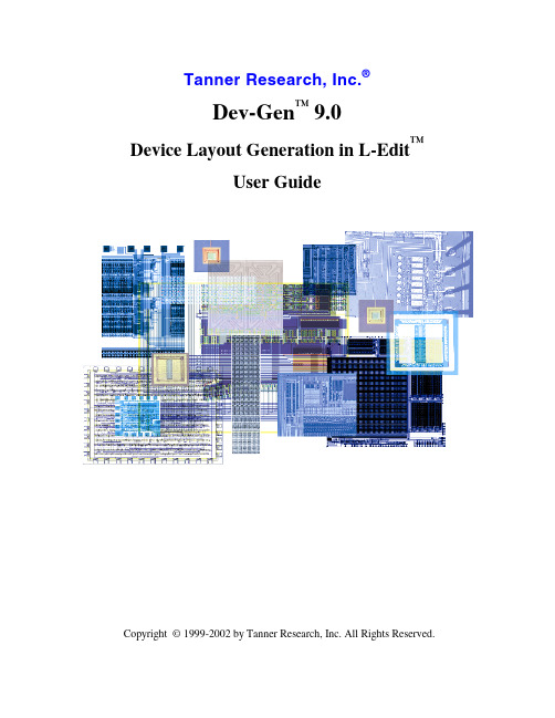
Tanner Research, Inc.®Dev-Gen™ 9.0Device Layout Generation in L-Edit™User GuideCopyright © 1999-2002 by Tanner Research, Inc. All Rights Reserved.Table of ContentsTable of Contents (2)Introduction (4)Running Dev-Gen (4)Device Setup (4)Using the Setup Dialogs (5)Importing and Exporting Device Settings (6)Device Setup Wizards (7)Modifying Device Parameters (8)Cell Info Placement Wizard (8)Capacitors (9)Inductors (11)Square Layout (12)Circular Layout (12)Resistors (14)Calculating Resistance (15)Segmented Resistor (16)Continuous Resistor (16)MOSFETs (18)Device Parameters (18)Layout Patterns (19)Additional Options (19)Setup Reference (21)Introduction (21)Capacitors (21)Text Formats (21)Single Capacitor Layer Setup (22)Single Capacitor Design Rules (23)Capacitor Array Layer Setup (25)Capacitor Array Design Rules (26)Default Parameters (28)Inductor Setup Wizard (29)Text Formats (29)Inductor Layer Setup (29)Inductor Design Rules (30)Default Parameters (31)Resistor Setup Wizard (32)Text Formats (32)Continuous Resistor Layer Setup (33)Continuous Resistor Design Rules (34)Segmented Resistor Layer Setup (35)Segmented Resistor Design Rules (36)Default Parameters (37)N- and P-Channel MOSFET Setup (38)Text Formats (38)MOSFET Layer Setup (39)MOSFET Design Rules (40)Default Parameters (43)IntroductionDev-Gen™ 9.0 is an integrated set of macros that provides parameterizable device layout generation in L-Edit, allowing ASIC designers to generate analog device layout quickly and accurately. For each device, you can specify layout configurations, design rules, and electrical parameters. The current macro set includes four device generators:• Capacitor Generator – constructs a single capacitor or a capacitor array.Optional dimension control allows you to constrain one dimension to a fixedvalue or create a square capacitor.• Inductor Generator – constructs inductor cells in either rectangular or circular coils. Parameters include the width of inductor segments and thetotal number of wraps in the coil.• Resistor Generator – constructs continuous (simple) or segmented(precision) resistor cells. Dimension control allows you to specify the widthand number of resistive layout segments.• MOSFET Generator – constructs n- or p-channel MOSFET cells using specified transistor parameters and layout options. Optional dimensioncontrol allows you to constrain one dimension of the device to a fixed value. Running Dev-GenThe suite of macros is accessible from the L-Edit menu by selecting Tools > Add-Ins > Dev-Gen.You can map Dev-Gen to a shortcut key by selecting Setup > Application from the L-Edit menu. On the Keyboard tab, choose the Macro category and select Dev-Gen from the list of available macros. Press the new shortcut key and click Assign.Dev-Gen device generation is highly dependent on the process technology. A series of dialogs is provided on the Setup tab of the Dev-Gen interface to guide you through the process technology setup. The first time Dev-Gen is launched on a layout database file, you will be prompted to begin setup by completing the Setup dialogs, importing settings from a text file, or accepting the default settings. After the initial setup, Dev-Gen device parameters are stored in the layout database file.Device SetupThe first step in using Dev-Gen is initializing the generator for the current layout database file (*.tdb). If you load Dev-Gen in a layout file that has not been initialized for Dev-Gen, a Missing Information dialog will prompt you to load or create the missing Dev-Gen setup parameters:Choose one of the following options:Import Dev-Gen information from a file Allows you to load a text file containing a list of Dev-Gen option values. Text files are discussed in Importing and Exporting Device Settings on page 6.Start editing Dev-Gen information by using the Dev-Gen setup wizard Launches the Dev-Gen Setup dialog. From the main setup dialog, you can launch individual wizards to specify parameters for each Dev-Gen device. When you have completed setup, click Cancel to close the Setup dialog and launch the standard Dev-Gen interface.Initialize Dev-Gen Information with default values Launches Dev-Gen with the default parameter values loaded.Once setup is complete, Dev-Gen device parameters are saved in the current .tdb file. Using the Setup DialogsDev-Gen includes a set of device setup wizards that allow you to create custom Dev-Gen device setups, each containing a set of saved parameter values. Tanner Research also includes Dev-Gen device setups in its popular Mixed-Signal Design Kits.To create or modify a set of device parameters, click the Setup tab of the Dev-Gen interface and select one of the device setup wizards. The Setup tab contains wizards for capacitor, inductor, resistor, and n- or p-channel MOSFET devices.Importing and Exporting Device SettingsThe Setup dialog includes Import and Export buttons that allow you to read and save setup information in a text file. Using the import and export functions, you can easily save parameters to share with other L-Edit/Dev-Gen users.To export setup information, click Export on the Setup tab. In the Export Dev-Gen Information To dialog, type or select the text file (*.txt) in which to save setup information and click Save. If you select an existing file, Dev-Gen will automatically overwrite its contents with the most recent setup data. The exported text file contains all parameters and configurations that have been specified in setup wizards for the current layout database (.tdb) file. The text file also contains the most recently used values in each cell generator dialog.To import setup information, click Import on the Setup tab. In the Import Dev-Gen Information From dialog, select a text file containing Dev-Gen setup information andclick Open.The easiest way to edit setup information is using the device setup wizards, describedbelow. However, you can also create a text file for import or edit an exported text filedirectly. Text file formats are described for each set of device parameters in SetupReference on page 21.Device Setup WizardsClicking a device setup wizard button launches the Setup Wizard dialog for that device:The Setup Wizard allows you to create or modify device names. Each Device Namecorresponds to a device class, a saved set of device parameters. You can specify severaldifferent setup configurations using different device names.Options include:Current Device Name Displays the currently selected device name. This field alsospecifies the name of the default setup configuration, whichis automatically loaded into the corresponding devicegenerator dialog’s Device Name field.Modify Launches the device setup wizard for the selected devicename. The device setup wizard is a series of dialogs thatwill guide you through the selection of layer assignments,design rules, and default electrical and geometricparameters.Create Launches the Create New Device Class dialog to create anew device name.Type the device name in the field provided and click OK.The device class will be created with Dev-Gen defaultvalues and saved in the current .tdb file. Click Modify toedit the default settings.Remove Deletes the selected Device Name and its associated setupconfiguration from the current .tdb file.Copy To…Creates a new device class using the same setupconfiguration as the selected device name.Rename To…Renames the selected device class.Modifying Device ParametersWhen you select a device name in the Setup Wizard and click Modify, Dev-Gen launches a series of setup dialogs for the selected device class. Device setup wizard dialogs specify layer assignments, design rules for constructing cells, and default parameters. A complete list of setup parameters for capacitors, inductors, resistors, and n- and p-channel MOSFETs is given in the Setup Reference on page 21.Cell Info Placement WizardThe Cell Info Placement Wizard launches a setup dialog to specify the location and appearance of information ports in a generated cell. Information ports are optional text ports that report electrical and geometric parameters used to generate a device.Information port settings apply to all device types. Options include:Cell Information Text Layer Specifies the layer on which Dev-Gen places information ports in the generated cell.Cell Information Text Size Point size of the port text.Cell Information Text Orientation Select the placement of text within a port. Text can be right- or left- justified in the top, center, or bottom of a port.CapacitorsTo generate a capacitor, select the Capacitor tab in the Device L ayout Generator dialog.Device Name shows the name of the currently active device class. The capacitor generator constructs capacitor cells using the layer assignments, design rules, andelectrical parameters specified for the active device class. To change the device class, open the Capacitor Setup Wizard in the Setup tab.In the Capacitor Type field, select either Capacitor Array or Single Capacitor from the drop-down list. The Capacitor Array generator builds large and precision capacitors from evenly distributed arrays of small and accurate unit capacitor elements. Capacitor arrays are widely used in demanding analog circuit implementations such as switch-cap circuitry in filter applications. The advantages of such structures include precision value and uniform parasitic conditions on unit capacitor elements.Capacitor parameters include:Total Capacitance The total capacitance of the cell to be built.Unit Capacitance (Array only) The capacitance of each component of the array. This field is not available for a single capacitor.Dimension Choose one of the following options:• Fixed Height– Capacitor is constructed with thespecified height. Capacitor width is varied toachieve the correct area.• Fixed Width– Capacitor is constructed with thespecified width. Height is varied to achieve thecorrect area.• Square– The capacitor is built with equal heightand width. The size of the square depends upon thecalculated area.If Fixed Height or Fixed Width is selected, specify acorresponding height or width value in the DimensionLength field. Height and width are specified in technologyunits.Place cell information into generated cell When checked, writes capacitor parameters to text ports in the generated cell. (Use the Cell Info Placement Wizard on the Setup tab to specify the layer for information ports.)The default values of Total Capacitance, Unit Capacitance, and Dimension Length are specified in the Capacitor device setup wizard.Click Build to create the new capacitor cell. All cells built by Dev-Gen are locked; to unlock the capacitor cell, choose Cell > Info from the L-Edit menu and uncheck the Locked (no edits) option.InductorsTo generate an inductor, select the Inductor tab in the Device Layout Generator dialog.Device Name shows the name of the currently active device class. The inductor generator constructs capacitor cells using the layer assignments, design rules, and electrical parameters specified for the active device class. To change the device class, open the Inductor Setup Wizard in the Setup tab.Choose either a Square or Circular layout style. The parameters for each layout type are described below.The option Place cell information into generated cell causes Dev-Gen to write inductor parameters to port text in the generated cell. Use the Cell Info Placement Wizard on the Setup tab to specify the layer for information ports.Click Build to generate the inductor cell. All cells built by Dev-Gen are locked; to unlock the inductor cell, choose Cell > Info from the L-Edit menu and uncheck the Locked (no edits) option.Square LayoutWhen Square is selected as the L ayout Style , the following Inductor Parameters apply:Generation DirectionThe direction in which the inductor will be generated, beginning at the inside of the coil. Options are Clockwise and Counter Clockwise . Inductor widthWidth, in technology units, of the wire used to generate the inductor. Initial Segment LengthLength of the first straight segment of the inductor. Subsequent segments increase in length as the coil increases in size. Number of turns The number of times the coil makes a complete revolutionaround the first inductor segment. This value is one fourththe number of right angles in the inductor. The following figure illustrates inductor parameters for a square coil with two turns: Circular LayoutTo generate a circular coil layout, select Circular in theLayout Style pull-down menu. When Circularis selected as the L ayout Style , the following Inductor Parameters apply:Generation Direction The direction in which the inductor will be generated,beginning at the inside of the coil. Options are Clockwiseand Counter Clockwise .Inductor widthWidth, in technology units, of the wire used to generate theinductor. Initial Segment LengthEnd of Turn 1End of Turn 2Generation DirectionInductor WidthInitial Radius Length Length, in technology units, of the radius of the innermostcircle in the inductor coil.Number of turns The number of times the inductor coil completes a 360degree revolution around its center.Segments Per Ring The number of linear segments used to approximate eachcircular revolution of the inductor coil.The following figure illustrates inductor parameters for a circular coil with two turns:End of End ofTurn 1 Turn 2ResistorsTo generate a resistor, select the Resistor tab in the Device Layout Generator dialog.Device Name shows the name of the currently active device class. The resistor generator constructs capacitor cells using the layer assignments, design rules, and electrical parameters specified for the active device class. To change the device class, open the Resistor Setup Wizard in the Setup tab.In the Resistor Type field, select either a Continuous Resistor or a Segmented Resistor from the drop-down list.Continuous resistors are simple resistors in which the resistive layer segments are connected by unit cell arrays on the resistive layer. Continuous resistors are the simpler of the two resistor types, and they generally have higher accuracy as the device increases in size. For best resistance approximation, a continuous resistor should have an odd number of segments (or an even number of turns).Segmented resistors are constructed from individual resistor segments connected by metal. Segmented resistors are preferable for small-value and high-accuracy devices, especially when the ratio between resistors is critical to circuit performance.Additional resistor parameters include:Resistor WidthThe width, in technology units, of subsegments on the resistor layer. ResistanceResistance value of the completed device. Dimension of resistor celldetermined by Enter an integer value in the Number Of Segments field to select the number of equal-length resistor subsegments thatwill be used to construct the device. The height of thesegments is then calculated from the number of segments,width of each segment, and the desired resistance.Note: The Vertical Dimension option has not yet beenimplemented.Place cell information into generated cellWhen checked, writes resistor parameters to port text in thegenerated cell. Use the Cell Info Placement Wizard on theSetup tab to specify the layer for information ports. Calculating ResistanceThe layout for a Dev-Gen resistor is calculated using the specified resistor parameters and the following formula for total sheet resistance:Segmented ResistorUnit Cell Array forContinuous ResistorWL R ρ= where • ρ is the Resistivity value (in ohms per square) of the resistor device. You can specify this parameter in the last step of the Resistor Setup Wizard.• L is the total calculated length of all resistor segments, in microns. The relationship between total length and segment length is described in the next section.• W is the user-specified width of the resistor segments, converted to microns. • R is the user-specified total resistance .Total resistor length is determined from the resistance equation above. From this calculation, Dev-Gen then determines the lengths of resistor segments according the type of resistor and total number of segments.Note: Contact and Metal Inter-Connect layers are generally add negligible resistance tothe primary resistive layer. Therefore, these values are ingored in resistance calculations.Segmented ResistorIn a segmented resistor, inter-connection paths between adjacent segments do not contribute to the total length. In this case, segment length (dL ) is equal to the total length divided by the user-specified number of segments (N ):Nh TotalLengt dL = The height of the final resistor cell is equal to the sum of the segment length and the contact cell heights (h ), as shown below.Continuous ResistorThe total length of a continuous resistor is calculated as the length of the central line of the primary resistive layer geometry. In this case, two different segment lengths are included in the calculation: HH = dL + 2hNhTotalLengt dL dL =+2• dL is the length of a main segment of the resistor body.• dL2 is the length of the interconnection between two resistor segments. This value is derivedfrom the minimum spacing rule for the primaryresistive layer (SP ). Each main segment of the resistor is paired with a corresponding interconnection segment. The length of a single main segment and interconnection pair is equal to the TotalLength divided by the specified number of resistor segments.The length of the interconnection, dL2, is equal to the sum of the resistor width (W ) and the minimum spacing between resistor segments (SP ). Minimum spacing on the primary resistive layer is specified in the Resistor Setup Wizard .MOSFETsTo generate a MOSFET, select the MOSFET tab in the Device Layout Generator dialog:Device Name shows the name of the currently active device class corresponding to the selected Device Type(n-channel or p-channel). The MOSFET generator constructs MOSFET cells using the layer assignments, design rules, and electrical parameters specified for the active device class. To change the active n-channel or p-channel device class, open either the N-Channel MOSFET Setup Wizard or the P-Channel MOSFET Setup Wizard in the Setup tab.Select either a P-Channel or N-Channel MOSFET in the Device Type field.Device ParametersThe Restricted by Cell Dimension field allows you to select one of three ways to determine the dimensions of the MOSFET device:• Manual– Allows you to specify the length and width of a single channel, and the total number of channels included in the device.• Horizontal – Allows you to constrain the MOSFET device to a maximum horizontal size. Using the specified values for channel length and total transistor width, Dev-Gen calculates the maximum allowed number of channels and their correspondingwidths.• Vertical– Constrains the MOSFET to a specified vertical size. Using the specified values for channel length and total transistor width, Dev-Gen calculates the minimumallowed number of channels and their corresponding widths.When Manual is selected, the available parameters are:Channel Length The length of an individual channel (technology units).Single Channel Width The width of an individual channel (technology units).Total Transistor Width The combined width of all transistor channels(technology units).When Horizontal or Vertical is selected, the available parameters are:Channel Length The length of an individual channel (technology units).Multiple Channel Count The total number of transistor channels.Restricted Cell Dimension The fixed horizontal or vertical size of the completedMOSFET device (technology units).Layout PatternsDev-Gen supports the following layout patterns:S/D Inter-Connection Allows optional metal connection between source and drain.Gate Inter-Connection Specifies the pattern of interconnection between gate layersegments. You can choose no connection, parallelconnections along the top and/or bottom of the segments, orsnaked connection paths beginning at the upper or lower endof the leftmost segment.Bulk Contact Arrangement Specifies the desired arrangement of optional bulk-contactelements.Additional OptionsPlace cell information into generated cell When checked, writes MOSFET parameters to port text in the generated cell. Use the Cell Info Placement Wizard on the Setup tab to specify the layer for information ports.SPICE Parameter Back Annotation Allows SPICE parameters such as source/drain areas and perimeters to be extracted to an L-Edit Extract file. Click Browse EXT File to choose the extract definition file.Setup ReferenceIntroductionEvery device generated by Dev-Gen is a member of a device class. A device class is a pre-defined set of parameters that specify layer assignments, design rules, and default parameters for a device type. A device type can have multiple device classes; see Device Setup Wizards on page 7 for information about creating device classes.You can define and modify Dev-Gen device classes using the device setup wizards, which are available from the Setup tab. Alternatively, you can edit setup information in a text file that contains all of the Dev-Gen device class definitions that will be used with your layout database file.Setup for each device class includes the following information:• Layer assignments that map Dev-Gen layer names to existing layers in your L-Edit database file. Some Dev-Gen layers are optional (e.g., a dielectric implant in acapacitor); to omit an optional layer, assign it a value of NULL.• Design rules for constructing the device cell. It is important that you define design rules to be consistent with the rules saved in Tools > Setup DRC for the currentlayout database file, or those specified by your foundry. For example, if the capacitortop plate layer is mapped to Poly, then the minimum width of the top plate should begreater than or equal to the minimum width of Poly. Otherwise, Dev-Gen devicesmay generate DRC errors and/or fail to fabricate properly.• Default Parameters that define the default values of device generator parameters. In some cases, default parameters also include internal electrical parameters, such asresistivity.Additional setup information includes:• The names of the default device classes for capacitor, inductor, resistor, and N- and P-Channel MOSFET devices.• Information port parameters, including the layer on which ports are placed and the size and alignment of text.The following sections describe setup parameters for each device. At the beginning of each section, the text format for parameter definitions is shown.CapacitorsText FormatsCapacitor setup information consists of the following sections of text.// Default device nametCell_Info.Capacitor.ClassDefault::5::ActiveClass// Single Capacitor Layer SetuptCell_yerName::5::MapLayer ...// Single Capacitor Design RulestCell_::3::Value...// Capacitor Array Layer SetuptCell_yerName::5::MapLayer ...// Capacitor Array Design RulestCell_::3::Value...// Default ParameterstCell_Info.Capacitor.ClassName.InitalValue.Parameter::3::Value...Single Capacitor Layer SetupThe first two dialogs of the Capacitor Setup Wizard allow you to assign elements of the Dev-Gen single capacitor to layers defined in your L-Edit layout database:To assign a Target Layer, select from the drop-down list. The first entry in each most lists is NULL. To omit a capacitor feature from the generated cell, set the Target Layer to NULL. (If NULL does not appear on the list, you can enter it manually in the Target Layer field.)Dev-Gen Layer(Text Format Name) Definition Recommended Target LayersC TOP PLATE (C_TopPlate) Layer that forms the top plate of the capacitor. Poly2Mim-CapC BOTTOM PLATE (C_BottomPlate) Layer that forms the bottom plate of thecapacitor.Poly1Metal4Dev-Gen Layer(Text Format Name)DefinitionRecommended Target Layers C MASK (C_Mask) Dedicated dielectric implant for special capacitive performance (such as Thin Oxide).*Thin Oxide C SUBS (C_Subs) Well or substrate below the capacitor. This layer is not electrically connected to the capacitor.*Well Metal3C ID (C_Id) ID layer to extract device to netlist components.*Capacitor ID 1stMETAL (1stMetal) Metal connecting to the capacitor. Metal1 CONTACT (Contact)Contact CutContact* Optional layers may be omitted from the capacitor by mapping them to NULL.Single Capacitor Design RulesSteps 3 and 4 of the Capacitor Setup Wizard contain design rule values for constructinga single capacitor:The Value for each rule is defined in technology units. # Rule(Text Format Name)Description1Top Plate: Min Top Plate Width (Rule1)Includes three rules that comprise the capacitor width:• Minimum width of the top plate. • Minimum width of the bottom plate.Mi i idth f th it ID l if# Rule(Text Format Name)Descriptionone is defined.2 Top Plate: Min Top Platesurrounded by Bottom Plate(Rule2) Minimum width of the bottom plate area surrounding the capacitor’s top plate.3 Bottom Plate: Min Bottom PlateSurrounded by C Mask(Rule3) If a dielectric implant (mask) layer is defined, specifies the minimum width of mask layer required to surround the capacitor’s bottom plate.4 Bottom Plate: Min Bottom PlateSurround by C Subs(Rule4) Minimum width of the substrate layer area surrounding the capacitor’s bottom plate.5 Contact: Exact Contact Cut Size(Rule5)Exact width of contact cuts.6 Contact: Min Contact Spacing(Rule6) Minimum spacing allowed between contact cuts.7 Contact: Min Contact Surroundby Metal(Rule7) Minimum width of the metal layer area surrounding each contact cut.8 Contact: Min Contact Surroundby Top Plate(Rule8) Minimum width of the top plate area surrounding each contact cut.9 Contact: Min Contact Surroundby Bottom Plate(Rule9) Minimum width of the bottom plate area surrounding each contact cut.10 Contact: Min (Bottom Plate)Contact Spacing to Top Plate(Rule10) Minimum spacing between contact cuts on the bottom plate and the edge of the capacitor top plate.Capacitor Array Layer SetupSteps 5 and 6 of the Capacitor Setup Wizard allow you to assign elements of the Dev-Gen capacitor array to layers defined in your L-Edit layout database:To assign a Target Layer, select from the drop-down list. The first entry in each most lists is NULL. To omit a capacitor feature from the generated cell, set the Target Layer to NULL. (If NULL does not appear on the list, you can enter it manually in the Target Layer field.)Dev-Gen Layer(Text Format Name) Definition Recommended Target LayersC TOP PLATE (C_TopPlate) Layer that forms the top plate of the capacitor. Poly2Mim-CapC BOTTOM PLATE (C_BottomPlate) Layer that forms the bottom plate of the capacitor. Poly1Metal4C MASK (C_Mask) Dedicated dielectric implant for special capacitive performance (such as Thin Oxide).*Thin OxideC SUBS (C_Subs) Well or substrate below the capacitor. This layer isnot electrically connected to the capacitor.*WellMetal3C ID(C_Id)ID layer to extract device to netlist components.* Capacitor ID1st METAL(1stMetal)Metal connecting to the capacitor. Metal1CONTACT(Contact)Contact cut. Contact2nd METAL(2ndMetal)Metal connecting the 1st Metal and Via layers.* Metal2VIA Via cut.* Via1。

Cadence 使用参考手册邓海飞微电子学研究所设计室2000年7月目录概述 (1)1.1 Cadence概述 (1)1.2 ASIC设计流程 (1)第一章Cadence 使用基础 (5)2.1 Cadence 软件的环境设置 (5)2.2 Cadence软件的启动方法 (10)2.3库文件的管理 (12)2.4文件格式的转化 (13)2.5 怎样使用在线帮助 (13)2.6 本手册的组成 (14)第二章Verilog-XL 的介绍 (15)3. 1 环境设置 (15)3.2 Verilog-XL的启动 (15)3.3 Verilog XL的界面 (17)3.4 Verilog-XL的使用示例 (18)3.5 Verilog-XL的有关帮助文件 (19)第四章电路图设计及电路模拟 (21)4.1 电路图设计工具Composer (21)4.1.1 设置 (21)4.1.2 启动 (22)4.1.3 用户界面及使用方法 (22)4.1.4 使用示例 (24)4.1.5 相关在线帮助文档 (24)4.2 电路模拟工具Analog Artist (24)4.2.1 设置 (24)4.2.2 启动 (25)4.2.3 用户界面及使用方法 (25)4.2.5 相关在线帮助文档 (25)第五章自动布局布线 (27)5.1 Cadence中的自动布局布线流程 (27)5.2 用AutoAbgen进行自动布局布线库设计 (28)第六章版图设计及其验证 (30)6.1 版图设计大师Virtuoso Layout Editor (30)6.1.1 设置 (30)6.1.2 启动 (30)6.1.3 用户界面及使用方法 (31)6.1.4 使用示例 (31)6.1.5 相关在线帮助文档 (32)6.2 版图验证工具Dracula (32)6.2.1 Dracula使用介绍 (32)6.2.2 相关在线帮助文档 (33)第七章 skill语言程序设计 (34)7.1 skill语言概述 (34)7.2 skill语言的基本语法 (34)7.3 Skill语言的编程环境 (34)7.4面向工具的skill语言编程 (35)附录1 技术文件及显示文件示例 (60)附录2 Verilog-XL实例文件 (72)1Test_memory.v (72)2SRAM256X8.v (73)3ram_sy1s_8052 (79)4TSMC库文件 (84)附录3 Dracula 命令文件 (359)概述作为流行的EDA工具之一Cadence一直以来都受到了广大EDA工程师的青睐然而Cadence的使用之繁琐又给广大初学者带来了不少麻烦作为一位过来人本人对此深有体会本着为初学者抛砖引玉的目的本人特意编写了这本小册子将自己数年来使用Cadence的经验加以总结但愿会对各位同行有所帮助本册子的本意在于为初学者指路故不会对个别工具进行很详细的介绍只是对初学者可能经常使用的一些工具加以粗略的介绍其中可能还请各位同行加以指正1.1 Cadence概述Cadence是一个大型的EDA软件它几乎可以完成电子设计的方方面面包括ASIC设计FPGA设计和PCB板设计与众所周知的EDA软件Synopsys 相比Cadence的综合工具略为逊色然而Cadence在仿真电路图设计自动布局布线版图设计及验证等方面却有着绝对的优势Cadence与Synopsys 的结合可以说是EDA设计领域的黄金搭档此外Cadence公司还开发了自己的编程语言skill,并为其编写了编译器由于skill语言提供编程接口甚至与C语言的接口所以可以以Cadence为平台进行扩展用户还可以开发自己的基于Cadence的工具实际上整个Cadence软件可以理解为一个搭建在skill语言平台上的可执行文件集所有的Cadence工具都是用Skill语言编写的但同时由于Cadence的工具太多使得Cadence显得有点凌乱这给初学者带来了更多的麻烦Cadence包含的工具较多几乎包括了EDA设计的方方面面本小册子旨在向初学者介绍Cadence的入门知识所以不可能面面具到只能根据ASIC 设计流程介绍一些ASIC设计者常用的工具例如仿真工具Verilog-xl,布局布线工具Preview和Silicon Ensemble,电路图设计工具Composer,电路模拟工具Analog Artist,版图设计工具Virtuoso Layout Editor,版图验证工具Dracula最后介绍一下Skill语言的编程1.2 ASIC设计流程设计流程是规范设计活动的准则好的设计流程对于产品的成功至关重要本节将通过与具体的EDA工具Synopsys和Cadence相结合概括出一个实际可行的ASIC设计的设计流程图11是实际设计过程中较常用的一个流程接下一页图1 1 ASIC设计流程图这是深亚微米设计中较常用的设计流程在该设计流程中高层次综合和底层的布局布线之间没有明显的界线高层设计时必须考虑底层的物理实现高层的划分与布局规划同时由于内核Core的行为级模型有其物理实现的精确的延时信息使得设计者可在设计的早期兼顾芯片的物理实现从而可以较精确的估计互连的延时以达到关键路径的延时要求同时布局布线后提取的SDF文件将被反标到综合后的门级网表中以验证其功能和时序是否正确从该流程中可看出在实际设计中较常用到的Cadence的工具有VerilogHDL仿真工具Verilog-XL,电路设计工具Composer电路模拟工具Analog Artist,版图设计工具Virtuoso Layout Editor,版图验证工具Dracula和Diva以及自动布局布线工具Preview和Silicon Ensemble本册子将对这些工具作一个初步介绍如果读者想进一步了解某个软件的使用可参考本册子提供的相关在线文档以进一步熟练第一章Cadence 使用基础2.1 Cadence 软件的环境设置要使用Cadence,必须在自己的计算机上作一些相应的设置这些设置包括很多方面而且不同的工具可能都需要进行各自的设置读者如果遇到这方面的问题可以参考一下openbook中的Configuration Guides及各工具的userguide或者reference,其访问的方法是 main menu-> System Administration-> Configuration Guides但作为初学者只需进行以下几项设置1..cshrc文件的设置首先要在自己的.cshrc文件中设置Cadence软件所在的路径所使用的licence文件等下面的代码为.cshrc中设置的一个简单示例其中Cadence所在的目录为/EDA04/cds97a/Cadencesetenv CDS_ROOT /EDA04/cds97asetenv CDS_INST_DIR /EDA04/cds97aset path = ($path $CDS_INST_DIR/tools/dfII/bin$CDS_INST_DIR/tools/bin)setenv LM_LICENSE_FILE /EDA04/cds97a/share/license/license.dat 对于某些Cadence中的工具也必须在.cshrc中进行一些设置2..cdsenv文件设置.cdsenv文件中包含了Cadence软件的一些初始设置该文件是用Skill语言写成的Cadence可直接执行3..cdsinit设置与.cdsenv一样.cdsinit中也包含了Cadence软件的一些初始化设置该文件是用Skill语言写成的在Cadence启动时会首先自动调用这两个文件并执行其中的语句若仅为初学可以不编写这两个文件Cadence 会自动调用隐含的设置若想更改设置可参考一些模板文件进行编写在install_dir/tools/dfII/cdsuser 目录下有一些隐含的模板文件下面是一个简单的.cdsinit 文件;;;;;;;;;;;;;;;;;;;;;;;;;;;;;;;;;;;;;;;;;;;;;;;;;;;;;;;;;;;;; Tutorial .cdsinit file; By: Cris Reeser/Diane Goldberg; Created: October 10, 1995;; This initialization file contains the settings necessary to; successfully run the Cell Design tutorial. Some of these may; be redundant, if your site uses a site initialization file.; For further information on initialization files, read the; comments in the <install_dir>/samples/local/cdsinit file.;;;;;;;;;;;;;;;;;;;;;;;;;;;;;;;;;;;;;;;;;;;;;;;;;;;;;;;;;;;;;; Human Interface Environment SettingshiiSetFont("text" "-adobe-courier-bold-r-*-*-12-*")hiSetFormPosition(603:500)hinestLimit = 5hiSetUndoLimit(10)hiExpertMode(nil)window(1)->useScrollbars = twindow(1)->backingStore = tenvSetVal("layout" "xSnapSpacing" 'float 0.5)envSetVal("layout" "ySnapSpacing" 'float 0.5)envSetVal("layout" "segSnapMode" 'string "anyAngle")envSetVal("layout" "stopLevel" 'int 20)envLoadFile("./.cdsenv");;;;;;;;;;;;;;;;;;;;;;;;;;;;;;;;;;;;;;;;;;;;;;;;;;;;;;;;;;;;; Bindkey Settingsload(prependInstallPath("samples/local/schBindKeys.il"))load(prependInstallPath("samples/local/leBindKeys.il"));;;;;;;;;;;;;;;;;;;;;;;;;;;;;;;;;;;;;;;;;;;;;;;;;;;;;;;;;;;;; RESIZE CIW; CIW; Note, hiFlush() is used as a workaround to display problem with; resizing windows in SKILL.hiFlush()hiResizeWindow(window(1) list(3:3 750:200));;;;;;;;;;;;;;;;;;;;;;;;;;;;;;;;;;;;;;;;;;;;;;;;;;;;;;;;;;;;; Tutorial Customization;;;;;;;;;;;;;;;;;;;;;;;;;;;;;;;;;;;;;;;;;;;;;;;;;;;;;;;;;;;;setSkillPath(". techFiles"); Welcome the userfprintf(poport"************************************************\n")fprintf(poport "Welcome to the SRAM Compiler... %s\n"getShellEnvVar("USER"))printf( " \n" )printf( "Done with initialization.\n" )printf("************************************************\n ")printf( " \n" )printf( " \n" )从中可看出Skill语言的语法与C语言的较为类似经过一定的学习后就很容易掌握4.cds.lib文件的设置如果用户需要加入自己的库则可以修改自己的库管理文件cds.lib对于初次使用Cadence的用户Cadence会在用户的当前目录下生成一个cds.lib文件用户通过CIW生成一个库时Cadence会自动将其加入cds.lib文件中下面是一个简单的Cadence库管理文件cds.lib的示例DEFINE ourTechLib/EDAHOME01/students/dhf/sram/dual/ourTechLibDEFINE sram /EDAHOME01/students/dhf/sram/dual/sramDEFINE basic ${CDS_INST_DIR}/tools/dfII/etc/cdslib/basicDEFINE sample${CDS_INST_DIR}/tools/dfII/samples/cdslib/sampleDEFINE analogLib/EDA04/cds97a/tools/dfII/etc/cdslib/artist/analogLib DEFINE pCells /EDAHOME01/students/dhf/sram/dual/pCellsDEFINE hhh /EDAHOME01/students/dhf/sram/dual/hhh 其中DEFINE为库定义的保留字,ourTechLib sram等为所定义的库的名字最后的字符串为保存库的实际的物理目录5.技术库的生成技术文件库对于IC设计而言是非常重要的其中包含了很多设计中所必需的信息对于版图设计者而言技术库就显得更为重要了要生成技术文件库必须先编写技术文件技术文件主要包括层的定义符号化器件的定义层物理以及电学规则和一些针对特定的Cadence工具的规则的定义例如自动布局布线的一些规则版图转换成GDSII时所用到的层号的定义技术文件的编写可参考openbook中有关技术文件的介绍并参考相应的模板来进行其访问顺序为Main Menu->ICTools->Design FramWork II->Technology File Help附录1中有一个简单的技术文件示例技术文件编好以后就可以按照以下几步生成技术库1点击CIW中的File菜单选择其中的New项中的Library项如图21所示弹出图22所示的表格2在Name项中输入所需的名字如myTecLib保持如图所示的设置点击ok弹出如图23所示的对话框3在对话框中输入编好的技术文件名如my.tf这时技术文件必须在启动Cadence的当前目录点击ok4经过一段时间后在CIW的显示区会出现一个提示Library myTecLib is created successfully.对于非工艺库的生成与工艺库大体相同只是在22中选择attach toexited technology file,并在接下来的过程中选择相应的工艺库图21图22图236.显示文件display.drf的设置display.drf文件控制Cadence的显示其基本语法可参考openbook中的相应的介绍附录1中包含了一个display.drf的示例2.2 Cadence软件的启动方法完成了一些必要的设置对初学者只需设置.cshrc文件即可其他设置都用隐含设置等熟练了一些之后再进一步优化自己的使用环境就可以启动Cadence软件启动Cadence软件的命令有很多不同的启动命令可以启动不同的工具集常用的启动命令有icfb,icca等也可以单独启动单个工具例如启动Viruoso Layout Editor可以用layoutPlus来启动Silicon Ensemble可以用sedsm来启动以icfb为例先在UNIX提示符下输入icfb&再按回车经过一段时间就会出现如图24所示的CIW Command Interpreter Window窗口从CIW窗口就可以调用许多工具并完成许多任务CIW窗口是使用Cadence时遇到的第一个窗口是Cadence主要的用户界面它主要包括以下几个部分1Title Bar显示使用的软件名及log文件目录如图24中的最上一行 icfb-log:/EDAHOME01/students/dhf/CDS.log2Menu Banner3Output Area 输出Cadence对用户命令的反应4Input Line 可用来输入Skill命令5Mouse Bindings Line 显示捆绑在鼠标左中右三键上的快捷键6Scrolling bar to Scroll Through the Log FileCadence将许多常用工具集成在一块以完成一些典型的任务图25总结了一些常用的启动命令及其可使用的工具用户可根据自己的需要选择最少的命令集图2 4 CIW窗口图2 5 Cadence启动命令2.3库文件的管理启动了Cadence后就可以利用File菜单建立自己的工作库点击CIW窗口上的File菜单选定其中的New lib项弹出如图22所示的对话框输入库名并选择相应的工艺库然后选择ok,这时在CIW的显示区会出现如下提示The lib is created successfully!新建的库是一个空的库里面什么也没有用户可在库中生成自己所需的单元例如可以生成一个反相器单元并为其生成一个电路及一个版图视图其流程如下1选择File菜单中的New项并选择Cellview项则弹出如图2-6所示的对话框选择所需的库并输入单元名inv并选择视图类型Schematic再点击ok按钮则弹出如图27所示的窗口2用Add菜单中的Component命令调用analogLib中的单元输入PMOS和NMOS管以及电源和地如图28所示3点击Check and save 命令保存用同样的流程可生成inv的版图视图利用Tools中的library manager可以对库进行管理图26图27图282.4文件格式的转化Cadence有自己的内部数据格式为了与其他EDA软件之间进行数据交换Cadence提供内部数据与标准数据格式之间的转换点击CIW的File菜单中的Import可将各种外部数据格式转换成Cadence内部数据格式利用CIW 的File菜单中的Export可将各种Cadence内部数据格式转换成外部标准数据格式2.5 怎样使用在线帮助学习Cadence的最好教材是使用在线帮助Cadence的在线帮助是用openbook命令来启动的在UNIX提示符下输入openbook&并回车就可以启动在线帮助要拷贝在线帮助中的文件可以先按下control键并用左键进行选择然后用copy进行拷贝如果想要知道一些关于如何使用openbook的技巧可在系统提示符下输入openbook help &即可2.6 本手册的组成在本手册中将按照ASIC设计流程分别在第三章介绍高层的HDL工具例如Verilog仿真工具Verilog-xl第四章介绍电路图设计工具Composer及电路模拟工具Analog Artist第五章介绍自动布局布线Preview和SiliconEnsemble第六章介绍版图设计工具Virtuoso Layout Editor和验证工具Dracula 和Diva第七章将介绍Skill语言的编程第二章Verilog-XL的介绍人们在进行电子设计时较常用的输入方法有两种一种为硬件描述语言一种为电路图输入随着ASIC设计技术的发展以HDL作为输入的设计方法已成为ASIC设计的主流目前较常用的硬件描述语言有VHDL和Verilog两种相对而言Verilog在工业上用的较为平常故本小册子的讨论集中在Verilog上作为EDA设计的主流软件之一Cadence提供了对Verilog及VHDL 的强大支持尤其是Verilog,Cadence很早就引入了Verilog,并为其开发了一整套工具而其中最出色的当数Verilog的仿真工具Verilog-XL Verilog-XL一直以其友好的用户界面及强大的功能而受到广大Verilog用户的青睐本章将分五个方面一一对对其进行一个较为详尽的介绍3. 1 环境设置对于一般的Cadence的用户而言可能不需要进行任何设置就可启动Verilog-XL用户可输入下列命令看自己是否可访问Verilog-XLwhich verilog如果可以访问Verilog-XL,会有类似如下的反应/EDA04/cds97a/ tools/bin/verilog否则必须在.cshrc中用set path命令加入以上路径3.2 Verilog-XL的启动Verilog-XL的启动命令为verilog,它可以附带很多可选项下面是其各选项及其意义Valid host command options for verilog:-f <filename> read host command arguments from file-v <filename> specify library file-y <directory> specify library directory-c compile only-s enter interactive mode immediately-i <filename> input from command file-r <filename> restart from a saved data structure-l <filename> set log file name-k <filename> set key file name-u convert identifiers to upper case-t set full trace-q quiet-d decompile data structureSpecial behavioral performance options (if licensed):+turbo speed up behavioral simulation.+turbo+2 +turbo with second level optimizations.+turbo+3 +turbo+2 with third level optimizations.+listcounts generate code for maintaining information for $listcounts+no_turbo don't use a VXL-TURBO license.+noxl disable XL acceleration of gates in all modulesSpecial environment invocation options (if licensed):+gui invoke the verilog graphical environment 下面是几个简单的使用示例在UNIX提示符下输入这些命令即可启动Verilog-XLExample host commands to run VERILOG:verilog sio85.vverilog f1 f2 f3verilog -s sio85.vverilog -r save.dat -l run2.log -k run2.keyverilog -r save.dat -si commands.vicverilog -dqcr save.dat一般较常用的启动方法是verilog –s +gui –v libname –f scriptFile sourcefilename &其中libname为所使用的库的名字scriptFile为用可选项编写的命令文件3.3 Verilog XL的界面运行以上的启动命令后如果未发生什么错误就会弹出下图所示的用户界面这就是Verilog-XL的SimControl窗口,从该图形界面中可控制仿真的执行图3 1 Verilog-XL 的图形界面Verilog-XL的图形界面主要有以下几个窗口1SimControlSimControl窗口是主要的仿真控制窗口当用带有gui选项的verilog命令启动Verilog-XL时就会弹出这个窗口通过这个窗口用户可以显示设计的模块结构运行Verilog-XL命令设置及显示断点强行给变量赋值等等通过这个窗口可以实现用户与仿真的交互从而达到对仿真的控制2Navigator通过点击SimControl窗口右上角的星形图标即可激活Navigator窗口该窗口可用来图形化显示设计的层次设计中的实体及其变量3Signal Flow Browser4Watch Objects Window5SimWaveSimWave窗口可以用来显示已经选择并跟踪了的信号的波形3.4 Verilog-XL的使用示例介绍了Verilog-XL的启动和用户界面后下面我们将通过一个具体的实例来演示Verilog-XL的使用在附录2中有本示例所需的文件在本示例中将对一个SRAM模块SRAM256X8.v进行仿真在这个SRAM模块中又包含了一个子模块ram_sy1s_8052.v所调用的为TSMC的0.35um的库test_bench 为test_memory.v在该test_bench中首先对SRAM进行写然后进行读下面按照一个简单的流程来对这个SRAM进行模拟1在UNIX提示符下输入verilog -c -v tcb773s.v test_memory.v &来对源文件进行调试如果没有错误会显示0 Simulation events2没有错误之后就可以启动Verilog-XL的图形界面verilog –s +gui –v tcb773s.v test_memory.v &则会弹出如图32所示的窗口3跟踪自己所需要的波形信号4按运行按钮或在命令行输入原点并回车即可运行按停止按钮即可停止停止后波形会自动更新图323.5 Verilog-XL的有关帮助文件与Verilog-XL有关的帮助文件主要有以下一些Verilog-XL ReferenceVerilog-XL User GuideVerilog-XL TutorialSimCompare User GuideSimWave User GuideVPI User Guide and Reference (formerly PLI 2.0)PLI 1.0 User Guide and ReferencePLI Application Note: Back Annotation and Delay Calculation PLI Application Note: Using the Value Change LinkLMC Hardware Modeling Interface Reference and User Guide Graphical Output for the Verilog Product Family Reference SDF Annotator User GuideCentral Delay Calculator Algorithm GuideTiming Library Format ReferenceVerilog Language Sensitive Editor User Guide可通过如下顺序对这些文档进行访问Main menu->HDL Tools>Verilog-XL第四章电路图设计及电路模拟设计的输入除了可以用硬件描述语言如VHDL及Verilog外还可以用电路图输入在早期的ASIC设计中电路图起着更为重要的作用作为流行的EDA软件,Cadence提供了一个优秀的电路图编辑工具Composer Composer 不但界面友好操作方便而且功能非常强大电路图设计好后其功能是否正确性能是否优越必须通过电路模拟才能进行验证Cadence同样提供了一个优秀的电路模拟软件Analog Artist由于Analog Artist通过Cadence与Hspice的接口调用Hspice对电路进行模拟本章将介绍电路图设计工具Composer和电路模拟软件Analog Artist的设置启动界面及使用方法简单的示例以及相关的辅助文件以便读者能对这两种工具有一个初步的理解4.1 电路图设计工具ComposerComposer是一种设计输入的工具逻辑或者电路设计工程师物理设计工程师甚至PCB板设计工程师可以用它来支持自己的工作4.1.1 设置对于一般的Cadence的用户而言可能不需要进行任何设置就可启动Composer但有时必须设置快捷键否则所有的快捷键就会失灵给使用带来一些不便在设计时快捷键往往会有很大的作用此外在电路设计中可能需要用到一些符号库例如sample库basic库analogLib库只需在cds.lib文件中加入以下一段代码DEFINE basic ${CDS_INST_DIR}/tools/dfII/etc/cdslib/basicDEFINE sample${CDS_INST_DIR}/tools/dfII/samples/cdslib/sampleDEFINE analogLib/EDA04/cds97a/tools/dfII/etc/cdslib/artist/analogLib4.1.2 启动Composer的启动很简单在启动Cadence后从CIW窗口中打开或新建一个单元的Schematic视图就会自动启动Composer的用户界面用户即可在其中放入单元及连线以构成电路图4.1.3 用户界面及使用方法图41是Composer的图形界面在该用户界面中大部分面积是右下角的显示区左边的图标是一些常用的工具读者可以自己启动Composer然后熟悉一下Composer的用户界面下面将简单介绍一下电路图设计及符号Symbol设计的简单流程图4 1 Composer的用户界面图42是编辑电路图的一般流程为1首先用Component命令调用符号库中的元件来添加元件如图的nand32添加完所有的元件后就可以加入pin,可通过add菜单中的pin项来进行添加3布线及标线名可通过wire命令布线通过更改其属性标上线名4添加节点5加注释6加整体属性如一些自动布局布线属性图4 2 电路图设计的简单流程符号是用来代表元件的简单符号如反相器用一个三角形代替在Cadence中当上层调用下层单元和进行上下级映射时通常调用其符号所以符号在电路设计中起着很重要的作用与启动Schematic Editor类似通过在CIW窗口中新建或打开一个单元的symbol视图就可启动Symbol Editor图43是编辑符号的一般流程主要包括以下几步1在编辑区加入一些基本的图形2加入符号的pin3加入连接基本图形与pin的线4加入符号的标记如inv5加入选择外框6加入文本注释7更改整体属性图4 3 符号设计的简单流程4.1.4 使用示例在openbook中有一个关于Composer的教程如果读者需要经常用到电路图本人建议你不妨去走一遍那个教程对你一定会有帮助的该教程可安如下顺序进行访问Main Menu-> IC Tools->Tutorials-> Composer4.1.5 相关在线帮助文档Composer: Design Entry help4.2 电路模拟工具Analog ArtistCadence提供进行电路模拟的工具Analog Artist Anglog Artist通过调用Hspice进行电路模拟然后进行各种后续处理并显示结果4.2.1 设置在运行Analog Artist之前必须在.cshrc中设置以下语句setenv CDS_Netlisting_Mode Analog此外最好能从Cadence的安装目录的Analog Artist中拷贝与模拟器相应的初始化文件4.2.2 启动Analog Artist的启动方法有很多种可以从Composer的Tools菜单中执行也可以从CIW的Tools菜单中执行4.2.3 用户界面及使用方法图44是Analog Artist的用户界面关于具体的使用方法请参考openbook 中的相应手册但有一点想提醒大家大家使用的licence可能不允许使用Analog Artist如果在微所使用Analog Artist且用Hspice为模拟器似乎激励文件用cdsspice格式才可调通有兴趣的读者可以一试4.2.5 相关在线帮助文档与Analog artist相关的在线文档有Analog Artist Simulation HelpAnalog Artist Microwave Design HelpAnalog Artist Mixed-Signal Simulation HelpAnalog Artist Parametric Analysis HelpAnalog Artist Substrate Coupling Analysis (SCA) HelpAnalog Artist SKILL Functions ReferenceAnalog Expression Language ReferenceCadence SPICE ReferenceComponent Description Format User GuideFunctional Block Library ReferenceHSPICE/SPICE Interface and SPICE 2G.6 ReferenceSpectre ReferenceSpectre User GuideSpectreHDL ReferenceSpectreRF HelpSwitched Capacitor Design System HelpAnalog Artist Tutorial: Switched Capacitor DesignVerilog-A Reference通过顺序Main Menu->IC Tools->Analog and Mixed Signal Simulation可以访问Cadence 使用手册第五章自动布局布线第五章自动布局布线5.1 Cadence中的自动布局布线流程从第一章的ASIC设计流程中可看到设计输入经过综合和优化后就该对所生成的门级网表进行自动布局布线自动布局布线是连接逻辑设计和物理设计之间的纽带在自动布局布线前必须进行布局规划floorplan,在Cadence中进行布局规划的工具为Preview进行自动布局布线的引擎有四种Block EnsembleCell Ensemble Gate Ensemble和Silicon Ensemble其中Block Ensemble适用于宏单元的自动布局布线Cell Ensemble适用于标准单元或标准单元与宏单元相混合的布局布线Gate Ensemble适合于门阵列的布局布线SiliconEnsemble主要用在标准单元的布局布线中将Preview与四种引擎相结合可产生四种不同的自动布局布线环境和流程由于Silicon Ensemble(DSM)的功能很完全几乎可以完成所有复杂的自动布局布线的任务在考虑自动布局布线引擎时我们采用了Silicon Ensemble SRAM编译器所生成的用于自动布局布线的端口模型为Silicon Ensemble所要求的格式图51为采用Preview和Silicon Ensemble进行自动布局布线的流程图该流程主要由以下几个主要步骤组成1准备自动布局布线库在进行自动布局布线之前必须准备好相应的库该库中含有工艺数据自动布局布线用的库单元及显示信息库的格式必须为DesignFramework II的数据库格式可以由用户利用版图生成工具VirtuosoLayout Editor设计产生也可以来自一个由芯片制造厂家和EDA公司提供的LEF(Library Exchange Format)文件或者从GDSII生成2准备用来进行自动布局布线的网表用来进行布局布线的网表可以由硬件描述语言经过综合优化或由电路提取而来所有网表在进行自动布局布线前都必须首先生成对应的autoLayout视图view3用Preview进行布局规划Preview是 Cadence的布局规划器它可以用来规划物理设计从而在自动布局布线前预估物理实现的影响在Cadence中使用Preview与自动布局布线引擎相结合来进行自动布局布线4用Silicon Ensemble进行自动布局布线5对完成布局布线的版图进行验证生成的版图其连接性是否正确是否符合设计规则是否符合时序要求等等必须通过验证才能确定通过点击Verify&Report菜单中的相应项可对版图进行连接性设计规则验证并可生成SDFStandard Delay Format文件通过反标SDF文件可对原来的门级网表进行仿真从而确定其功能和时序是否正确图5 1 用Preview和Silicon Ensemble进行自动布局布线的流程5.2 用AutoAbgen进行自动布局布线库设计对于不同的自动布局布线引擎,对应的库的数据格式有所不同,用来生成库的工具也不同本SRAM编译器选择Silicon Ensemble作为布局布线引擎其对应的库生成工具为AutoAbgen AutoAbgen可以用来生成与用户设计的版图或版图库所对应的Abstract(即用于自动布局布线的端口模型)可以用AutoAbgen的AutoAbgen Flow Sequencer form来生成Abstract对于单个版图和LEF文件对于整个物理库其基本流程如下(1)首先在局部.cdsinit中设置好AutoAbgen运行的环境即在.cdsinit中加入以下语句aabsInstallPath=“<install_dir>/tools/autoAbgen/etc/autoAbgen”load(buildstring(list(aabsInstallPath “aaicca.ile”) “/”))(2)将AutoAbgen的初始化文件.autoAbgen拷入运行目录并用icfb&启动Cadence(3)点击CIW窗口中的AutoAbgen菜单下的AutoAbgen Flow Sequencer项打开Flow Sequencer Form(4)选择合适的流程(5)建立布局布线所需的工艺信息如果在工艺文件中已经包含布局布线的工艺信息可以忽略这一步(6)建立用来生成Abstract的版图数据如果所用的版图数据已经是DFII 的版图格式可以忽略这一步(7)更新单元的属性及其管脚属性由于AutoAbgen对所操作的版图有些特殊要求所以在生成Abstract前必须对其属性进行更新以符合AutoAbgen的要求(8)建立一个库单元将所需建立Abstract的所有单元包括到里面(9)填写环境设置表格和运行选项表格输入输出LEF的文件名如果是对库进行操作(10)选择Apply运行AutoAbgen生成所需的Abstract第六章 版图设计及其验证版图设计及其验证如果有人问Cadence 最突出的优点在那里我想问题的答案应当就在本章可以说,Cadence 的版图设计及验证工具是任何其他EDA 软件所无法比拟的Cadence 的版图设计工具是Vituoso Layout Editor,即为版图编辑大师以下简称版图大师版图大师不但界面很漂亮而且操作方便功能强大可以完成版图编辑的所有任务版图设计得好坏其功能是否正确必须通过验证才能确定Cadence 中进行版图验证的工具主要有Dracula 和Diva 两者的主要区别是Diva 是在线的验证工具被集成在Design Frame Work II 中可直接点击版图大师上的菜单来启动而Dracula 是一个单独的验证工具可以独立运行相比之下Dracula 的功能比较强大6.1 版图设计大师Virtuoso Layout Editor版图设计大师是Cadence 提供给用户进行版图设计的工具其使用起来十分方便下面进行一个简单介绍6.1.1 设置版图大师的设置很简单对于一般的Cadence 的用户而言可能不需要进行任何设置就可启动版图大师但有时必须设置快捷键否则所有的快捷键就会失灵给使用带来一些不便在设计时快捷键往往会有很大的作用与电路设计不同的是版图设计必须考虑具体的工艺实现因此存放版图的库必须是工艺库或附在别的工艺库上的库否则用隐含的库将没有版层即LSW 窗口只有一个黑框更无从画图了因此在设计版图前必须先建立自己的工艺库此外显示对于版图设计也很重要因此最后有自己的显示文件display.drf6.1.2 启动有很多种方法自动版图大师最简单的办法是通过CIW 打开或者新建一。
STICK OVERVIEWA. POVB. Mini Analog StickC. Thumb HATs, Witches andCastleD. Stick Buttons with Triggerand 2 x Head Buttons E. X, Y, and Rz Axes, Elevator,Aileron and Rudder AxesF. Pinkie and Flying PinkieG. F.E.E.L. Spring SystemTHROTTLE OVERVIEWA. Throttle Rotaries with inset buttonsB. 2-position SliderC. Thumb Controls with 2 HATs, Thumb Button,Mini AnalogStickD. Twin Throttles with Throttle LockE. Throttle Tension AdjusterF. 3-position Mode SwitchG. Base Controls with 7 Toggles and 2 RotariesGETTING STARTEDDrivers and Software InstallationWindows® 7/8/101. Download and install the X56 HOTAS software from /support/x562. After reading the Disclaimer, select the 'I accept the terms of the Disclaimer' optionand click 'NEXT' to continue3. At the Plug In screen, plug the Stick and Throttle units into the PC. Click ‘Next’ whenit becomes highlighted4. From the end screen, click ‘Finish.’ Your drivers and software are now installedNET Framework1. If this is the first Logitech product that you have installed, you may be asked to install.NET Framework after the software installation finishes. This is strongly recommended;this Microsoft Feature Update is required by the Software2. Click ‘Download and install this file.’ The PC will now find the correct files fromthe Internet and download them3. When the installation finishes, click ‘Close’CONTROLLER SETTINGSIf at any time you wish to check that the X56 is working correctly, open the Game Controllers page and click on the controller’s Properties tab.Here are the various ways to do this from each operating system:Windows® 8/101. From the Metro/Start screen, click the ‘Control Panel’ icon. NOTE: If you haveno Control Panel icon on your Metro/Start screen, type ‘control panel’ and the iconfor the Control Panel will appear2. Once the Control Panel is open, double-click on the ‘Devices and Printers’ icon.NOTE: If you cannot see this icon, make sure that you have large icons selected3. With the Devices and Printers screen open, find the X56 HOTAS in the device list and right-click on this icon. From the dropdown menu, select ‘Game Controller Settings’4. From the Game Controllers window, you should see the X56 HOTAS. listed and selected.Click ‘Properties’ and this should take you to the Controller Test screenFrom the Controller Test screen you can test all the functions, axes, buttons, rotaries, etc. When you have completed your tests, click ‘OK’ twice to get back to the main desktopWindows® 71. Click on the ‘Windows’ icon from the system tray. Hover over the All Programs menu.Click the ‘Games’ folder and then the ‘Games Explorer’ icon2. Click the ‘Tools’ option (with downward facing arrow) from the list across the topof the window. From the dropdown list, click ‘Input Devices’3. From the Game Controllers window, you should see the X-56 Rhino listed and selected.Click ‘Properties’ and this should take you to the Controller Test screenF.E.E.L. Spring Tension SystemEach spring placed on the Rhino stick shaft will give a different feeling. You can also operate the stick without a spring, providing a total of five different forces.Each spring has a unique feel and different identification. These identifiers are color swatches at the top of each spring – Red, Yellow, Blue, and Green. This table lists some of the calculations used for differentiation:Changing or removing a springTo insert, change, or remove a spring, follow these steps. Ensure the trigger is facing away from you and that the X56 HOTAS logo plate is facing you.1. Turn the Locking Bezel (part B) counterclockwise until the Stick comes away from the base.2. Remove the Seal Ring (part C) by placing the fingers from your left and right hand under the ring on either side, and then lift up. The Seal Ring is stiff by design.3. Pry apart the Locking Clamps (part D). These pull apart from the stick, but are under load from the spring. Take one half off first, hold the spring, and then remove the other half.4. Remove the Spring (part E), then either replace with a new Spring of leave the Spring off.To reassemble, reverse the order of the above steps, making sure to securely seat the Seal Ring (Part C) and firmly tighten the Locking Bezel (part D) on the Stick base.Note: When changing springs, please ensure that the USB cable is disconnected from your PC and avoid touching the connectors in the stick handle and base.1. Turn Locking Bezel counterclockwise 4. Pry apart Locking Clamps2. Remove Stick 5. Remove Spring3. Remove Seal RingSoftware OverviewThe software allows you to program the X56 with an array of keyboard commands, from basic single-key commands to very advanced, timed, and macro commands. It will also allow you to program any axis with keyboard commands, and program mouse commands.In the software you can also alter the response curves and deadbands of the main axis – we’ll cover the explanation of these topics later in the manual.There are two ways to launch the software:1. From the desktop icon that looks like this2. From the start menu bar...Once the software launches, you will be presented with the Home Screen.If it’s the first time you’ve run the software, you will be asked to choose your language. Once this is done the main Home Screen will appear. If you’ve made a mistake choosing your language or you wish to choose another language, the language menu can be accessed by clicking on the icon in the bottom-right corner of the Home Screen.There are three main Tabs within the software:1. HOME2. PROGRAMMING3. SE TTINGSHOME TABOn the Home screen you’ll see:- Live Facebook feed from Logitech G- Social media and website shortcuts, , Twitter, YouTube, Instagram, etc - Language selection, use the flag icon in the bottom-right corner to access thisPROGRAMMING TABAfter selecting the PROGRAMMING Tab you will see the X56’s programming environment.You will see a high-resolution image of the controller you are going to program on the left side of the screen. On the right side of the screen you will see a list of command boxes, called “Cells,” going down the page.At the top of the image panel you will see Stick and Throttle icons. Clicking on eitherof these will change the current unit you are programming. The unit you are programmingis easily recognizable by the larger image that fills the window.In the PROGRAMMING Tab you can mimic your controller to directly copy any of the keyboard commands used in your favorite games. The commands are then saved in what we call a Profile. What is a Profile?A Profile is the name given to a file that has programmed controller commands saved intoit. For example, you may have a Joystick with a number of buttons/hats. If you want one of these to do something in-game that you would normally have to use a keyboard shortcut for, you can “assign” that command to that button. If you want Button ‘A’ to activate the landing gear (which is the “G” key on a keyboard), you can use the software to assign this function. You can also create more complicated assignments, like “shift+F2,” or even timed commands and macros.Making your first Profile1. Either hover the mouse pointer over the Cell, or press the button you want to create a Profilefor on the controller. If you hover your mouse over the Button ‘A’ Cell, Button ‘A’ will light up on the 3D Joystick image. Or just click Button ‘A’ on the stick and the correct Cell will light up.2. W hen the correct Cell is lit, left-click in itand a large flashing cursor will appear inthe left side of the Cell. You will also seea green tick, a red cross, and a mouse iconon the right side of the Cell.3. T he Cell is now waiting for the keyboardcommand. Using your keyboard, pressthe button on the keyboard you wouldlike Button ‘A’ on the stick to activate.For this example we will use the ‘G’ key,which usually activates landing gear.When you press ‘G’ on the keyboard, a largewhite tile with the letter ‘G’ should appearin the Cell, as shown here. If this is the correctkeyboard command, press the green tick iconon the right side. If not, press the red crossand redo the procedure to get the keyboardcommand into the Cell again.4. A fter pressing the green tick icon,the command name box will appear,labeled as “Untitled” (left image, below).Simply choose a name for the commandand type the name into this box.For this example, we chose “Landinggear.” Press the enter key to complete theCell. Button ‘A’ = Landing gear, which isyour keyboard’s ‘G’ key (right image, below).5. T est your Profile by opening the “Testing”window. Above the 3D image there areseven icons. The one that is second fromthe right, which looks like a silver cog,is labeled “Test Profile.”C lick on this icon and a new window willopen. A cursor will already be flashingin the test area. Simply press Button ‘A’on the X56. When this is pressed, letter ‘G’will appear in the window, which provesyour first programmed button is working.C lose this window by clicking on the “OK”icon in the bottom-right corner ofthe Testing window.6. You can add other keyboard commands if you wish and then test them. Just rememberto save your work before you shut down the software.7. T o make the programming you have just created workin your game, you must first save it as a Profile and thenactivate it. This can be done with one click. In the icon rowjust above the 3D image, you will see an icon that looks likea blue target. If you hover over this icon a tool tip labeled“Profile” will appear.C lick this icon and a standard Windows save box will appear.Give your Profile a name and save it. After saving, the Profilewill become active and you can shut down the softwareand play your game. The X56 will now respond as you haveprogrammed it.8. The software is capable of many other powerful programming features that we have notyet covered. For example, you can program axes, mouse movement and mouse buttons, hats, and special timed or complicated commands.123567Icons in the Profile Editor1. New ProfileOpens a blank Profile for you to edit/build.2. Open ProfileOpens a previously created Profile for editing.3. Save ProfileClicking “Save” will save a new Profile or overwrite a current Profile.Using the drop-down arrow next to “Save,” you can “Save as,” allowing you to savethe current Profile to a different location or as a different name.4. ViewsYou can change the view in the Profile Editor to be just programming Cells (i.e., no image).Clicking the “Views” button again will restore the default view and the image will reappear.5. ProfileIf you are working on a Profile to use immediately, so you can get flying straight away, click here.6. Test ProfileClicking this icon will bring up the test window. This is especially useful if you are attempting to program advanced timed or macro commands as it gives you a place to test your work before you fly.7. PrintBy pressing this icon, the Profile that you are currently building will be sent to the default printer on your system.SettingsThe settings page will allow you to alter the deadzone and response curves of all axes on both the Stick and the Throttle.Response CurvesDepending on the type of aircraft that you fly, you may want your joystick to be more or less sensitive around the middle or end points of the axes. For example, if you’re flying an F/18on a refueling mission at 25,000 feet, you will be making very fine movements to get intothe correct position. Having a shallower response curve around the center point of the joystick’s X and Y axes will enable you to make very fine adjustment to your aircraft.DeadbandsA deadband, sometimes known as a deadzone or neutral zone, is a part of the range in which an axis moves, undetected by the drivers and without effect on in-game progress. It may be around the center point of the axis range, or at either end of the axis range.Axis Range AdjustmentThe axis range adjustment, or axis saturation to assign its correct name, allows you to shrink the raw data range of an axis.Physical Axis AdjustmentThe physical axis adjustment, or physical saturation, allows you to shrink the full axis data range into a small physical stick movement.S-Curves and J-CurvesThere are two types of adjustable curves – S-Curves and J-Curves. J-Curves are linear axes,like throttles and rotaries. S-Curves are non-linear, like X and Y axes.The first screenyou’ll see is the ‘SELECTDEVICE TO MODIFY’screen.You have two choices;choose to alter eitherthe Stick or the Throttleaxis.Once you are in the ‘STICK // AXIS MODIFICATION’ screen, you’ll see a raft of options. We’ll go through them one by one.121. Name of the Part being Modified2. Modifiable Axes3. Manual Axis Adjustment and Test Area4. Spring Values – for Reference when Changing Axis Data5. Back Button6. Physical Axis Adjustment Slider7. Manual Axis Attribute Boxes8. Deadzone Adjustment9. Axis Curvature Adjustment10. Pre-made Profiles11. Apply Button12. Undo Button1. Name of the Part being ModifiedThis will either be the Stick or the Throttle unit for the X-56. If you wish to change the part that you’re not currently on, use the back button (5) to go back to the selection screen.2. Modifiable AxesThis shows a list of all modifiable axes. The Stick has three modifiable axes:- X Axis- Y Axis- Rudder AxisThe Throttle unit has six modifiable axes:- Left Throttle- Right Throttle- Rotary 1- Rotary 2- Rotary 3- Rotary 43. Manual Axis Adjustment and Test AreaThis area will show you how the current response curves / dead zones / saturation points are set up on the selected axis. You can also adjust the center deadzone, the range saturation, physical saturation, and the response curve on the selected axis. There is also a cross-hair which will show the physical position of the axis you are manipulating.4. Spring ValuesThis is a reference section when you are adjusting the axes on the Stick. It will act as a guide for axis modification, and you may choose differing axis curves or deadzones depending on the Spring you have fitted to the Stick. If you are modifying the Throttle unit’s axes you will not see this reference section.5. Back ButtonTakes you to the device selection screen.6. Physical Axis Adjustment SliderAllows the ends of the axes, the far left and far right on the X Axis or full up and full down on the Y Axis, to be moved inwards towards the center point. It is similar to setting up a deadzone at the far ends of your axis.7. Manual Axis Attribute BoxesThis area allows you to input raw data to setup your deadband, curvature, range saturation, and physical saturation settings. This is very useful if you already have the data or a third-party source is supplying the data. For example, a forum post on how to setup the response curve for an F/A-18F.8. Deadzone AdjustmentThe deadzone slider will allow you to adjust the deadzone around the center point of the axis you currently have selected.9. Axis Curvature Adjustment SliderShrinks the range of an axis. Instead of going from 0 to 65555, for example,we can shrink it to 300 to 62555.10. Pre-made ProfilesWe have included a set a predefined curves to select. This is to make it easier for those whodo not wish to make their own curves. There are two different types of curves to choose from:1. J-Curves – these curves will give you a single point of manipulation and are ideal for throttlesa nd rotaries.2. S-Curves – these curves will give you two points of manipulation and are ideal for settingup X and Y axes.11. Apply ButtonThis button will save the curve that you are manipulating on the selected axis. Once saved, this axis will perform as saved, for all games, until the axis is adjusted and resaved or the reset button is used.12. Undo ButtonThis button will turn the response curves on your currently selected axis back to their default state. This can be very useful when experimenting with curves and deadbands.Altering Axis AttributesAxis Status NotificationsYou’ll need to be aware of several notifications in the axis highlighter box when manipulating and applying axis data. On the left is a list of the current device’s axes. The colors indicatethe status of each axis.Light Blue in the larger box indicates the currently selected axis.Green in the smaller box indicates that the data on the settings pageand the data on the device are in sync for this axis.Y ellow in the smaller box indicates that the data for this axis has beenmodified on the settings page but has not yet been synced to the device.To sync data, click ‘Apply’ in the bottom right. The entire box will turnY ellow then start to fill up Green to indicate that the data on the settingspage is being synced to the device. Once data is fully synced, the largerbox will revert to Light Blue and the smaller box will stay Green.When the Axis box turns Green, the data from the settings pagesaves to the physical device. The main Axis box will then turn Blue andthe slash will turn to Green.Setting a DeadzoneTo set a deadzone on an axis, whether it’s an S-Curve or a J-Curve, simply move the deadzone slider (part 8). You will see the axis start to split from the middle in the manual adjust area. The deadzone will become larger as the slider moves farther.Setting a Response CurveTo set a response curve on an axis, whether it’s an S-Curve or a J-Curve, simply movethe curvature slider. On an S-Curve setting you will see the curve turn snake-like, which indicates curvature above and below the center point the axis.On a J-Curve setting you will see the whole axis curve as the slider moves. You can also change the curvature of either curve by moving the points in the manual adjustment area (part 4).If you move the points in the area, 2 for an S-Curve and 1 for a J-Curve, then the curve will adjust to the new points.Setting an Axis RangeTo set an axis range, simply move the Axis Range Adjustment Slider (part 5). This will shrinkthe data for that axis from the full negative side and from the full positive side. Now whenyou use the axis that you have just altered, the axis data output will only output up to the points that you have set in the settings.Setting a Physical AxisTo set the physical axis range on any axis, move the Physical Axis Adjustment Slider (part 6). Moving this slider will shrink the minimum and maximum range of the physical axis.After moving the sliders to set your axis, every time you move the physical axis you'll see that the minimum and maximum range has shrunk.Saving a SettingTo save settings so they're usable, click the ‘Apply’ Button in the bottom right-hand corner of the screen (part 13). Once you've hit ‘Apply,’ the axis icon (part 1) will turn Yellow,and progressively turn Green. A Green end segment and Blue main axis indicates saved data. For more details on axis notification, please check the ‘Axis Notifications’ section.TROUBLESHOOTINGQ1 My computer is not recognizing the Controller, what’s wrong?A 1. Have you downloaded and installed the drivers from ?A 2. Check the cable connections. Unplug your controller and plug it back in, making certainthat it is securely attached.A 3. If you’re using front or top facing USB ports, try plugging into the back of the PC.A 4. I f using a hub, make sure it’s a powered hub.Q2 Why doesn't the game I'm playing recognize my Controller?A 1. Ensure that you have conducted the checks in Q1 [above].A 2. Does the game you are playing offer support for game controllers? Please refer toyour game’s manual, which should contain information regarding the use of gamecontrollers. If it does not, you can use the powerful programming software to emulate the mouse and keyboard on your X56 HOTAS.Q3 One of the buttons or axes is not working on my controller.A 1. Please test your product in the Game Controllers panel as mentioned in the early partof this manual.A 2. If you are still experiencing problems with the controller, please contact the tech supportteam at /Tickets/SubmitQ4 In flight simulation games, like FSX, why doesn't my aircraft correctly respond to axes?A 1 The X56 HOTAS stick and throttle units are independent units, therefore they bothhave an X Axis, a Y Axis, etc. It is a simple case of going into the controller settings for your simulation game and setting up the X56 HOTAS. For a more detailed overview on how to do this please visit our FAQ page: /support/x56Q5 How do I change the X56 HOTAS LED color and brightness?A 1 Install the software to find a brightness slider under the SETTINGS tab.English 22。
Abrupt junction 突变结Accelerated testing 加速实验Acceptor 受主Acceptor atom 受主原子Accumulation 积累、堆积Accumulating contact 积累接触Accumulation region 积累区Accumulation layer 积累层Active region 有源区Active component 有源元Active device 有源器件Activation 激活Activation energy 激活能Active region 有源(放大)区Admittance 导纳Allowed band 允带Alloy-junction device合金结器件Aluminum(Aluminium) 铝Aluminum – oxide 铝氧化物Aluminum passivation 铝钝化Ambipolar 双极的Ambient temperature 环境温度Amorphous 无定形的,非晶体的Amplifier 功放扩音器放大器Analogue(Analog) comparator 模拟比较器Angstrom 埃Anneal 退火Anisotropic 各向异性的Anode 阳极Arsenic (AS) 砷Auger 俄歇Auger process 俄歇过程Avalanche 雪崩Avalanche breakdown 雪崩击穿Avalanche excitation雪崩激发Background carrier 本底载流子Background doping 本底掺杂Backward 反向Backward bias 反向偏置Ballasting resistor 整流电阻Ball bond 球形键合Band 能带Band gap 能带间隙Barrier 势垒Barrier layer 势垒层Barrier width 势垒宽度Base 基极Base contact 基区接触Base stretching 基区扩展效应Base transit time 基区渡越时间Base transport efficiency基区输运系数Base-width modulation基区宽度调制Basis vector 基矢Bias 偏置Bilateral switch 双向开关Binary code 二进制代码Binary compound semiconductor 二元化合物半导体Bipolar 双极性的Bipolar Junction Transistor (BJT)双极晶体管Bloch 布洛赫Blocking band 阻挡能带Blocking contact 阻挡接触Body - centered 体心立方Body-centred cubic structure 体立心结构Boltzmann 波尔兹曼Bond 键、键合Bonding electron 价电子Bonding pad 键合点Bootstrap circuit 自举电路Bootstrapped emitter follower 自举射极跟随器Boron 硼Borosilicate glass 硼硅玻璃Boundary condition 边界条件Bound electron 束缚电子Breadboard 模拟板、实验板Break down 击穿Break over 转折Brillouin 布里渊Brillouin zone 布里渊区Built-in 内建的Build-in electric field 内建电场Bulk 体/体内Bulk absorption 体吸收Bulk generation 体产生Bulk recombination 体复合Burn - in 老化Burn out 烧毁Buried channel 埋沟Buried diffusion region 隐埋扩散区Can 外壳Capacitance 电容Capture cross section 俘获截面Capture carrier 俘获载流子Carrier 载流子、载波Carry bit 进位位Carry-in bit 进位输入Carry-out bit 进位输出Cascade 级联Case 管壳Cathode 阴极Center 中心Ceramic 陶瓷(的)Channel 沟道Channel breakdown 沟道击穿Channel current 沟道电流Channel doping 沟道掺杂Channel shortening 沟道缩短Channel width 沟道宽度Characteristic impedance 特征阻抗Charge 电荷、充电Charge-compensation effects 电荷补偿效应Charge conservation 电荷守恒Charge neutrality condition 电中性条件Charge drive/exchange/sharing/transfer/storage 电荷驱动/交换/共享/转移/存储Chemmical etching 化学腐蚀法Chemically-Polish 化学抛光Chemmically-Mechanically Polish (CMP) 化学机械抛光Chip 芯片Chip yield 芯片成品率Clamped 箝位Clamping diode 箝位二极管Cleavage plane 解理面Clock rate 时钟频率Clock generator 时钟发生器Clock flip-flop 时钟触发器Close-packed structure 密堆积结构Close-loop gain 闭环增益Collector 集电极Collision 碰撞Compensated OP-AMP 补偿运放Common-base/collector/emitter connection 共基极/集电极/发射极连接Common-gate/drain/source connection 共栅/漏/源连接Common-mode gain 共模增益Common-mode input 共模输入Common-mode rejection ratio (CMRR) 共模抑制比Compatibility 兼容性Compensation 补偿Compensated impurities 补偿杂质Compensated semiconductor 补偿半导体Complementary Darlington circuit 互补达林顿电路Complementary Metal-Oxide-Semiconductor Field-Effect-Transistor(CMOS)互补金属氧化物半导体场效应晶体管Complementary error function 余误差函数Computer-aided design (CAD)/test(CAT)/manufacture(CAM) 计算机辅助设计/ 测试/制造Compound Semiconductor 化合物半导体Conductance 电导Conduction band (edge) 导带(底) Conduction level/state 导带态Conductor 导体Conductivity 电导率Configuration 组态Conlomb 库仑Conpled Configuration Devices 结构组态Constants 物理常数Constant energy surface 等能面Constant-source diffusion恒定源扩散Contact 接触Contamination 治污Continuity equation 连续性方程Contact hole 接触孔Contact potential 接触电势Continuity condition 连续性条件Contra doping 反掺杂Controlled 受控的Converter 转换器Conveyer 传输器Copper interconnection system 铜互连系统Couping 耦合Covalent 共阶的Crossover 跨交Critical 临界的Crossunder 穿交Crucible坩埚Crystal defect/face/orientation/lattice 晶体缺陷/晶面/晶向/晶格Current density 电流密度Curvature 曲率Cut off 截止Current drift/dirve/sharing 电流漂移/驱动/共享Current Sense 电流取样Curvature 弯曲Custom integrated circuit 定制集成电路Cylindrical 柱面的Czochralshicrystal 直立单晶Czochralski technique 切克劳斯基技术(Cz法直拉晶体J)Dangling bonds 悬挂键Dark current 暗电流Dead time 空载时间Debye length 德拜长度De.broglie 德布洛意Decderate 减速Decibel (dB) 分贝Decode 译码Deep acceptor level 深受主能级Deep donor level 深施主能级Deep impurity level 深度杂质能级Deep trap 深陷阱Defeat 缺陷Degenerate semiconductor 简并半导体Degeneracy 简并度Degradation 退化Degree Celsius(centigrade) /Kelvin 摄氏/开氏温度Delay 延迟Density 密度Density of states 态密度Depletion 耗尽Depletion approximation 耗尽近似Depletion contact 耗尽接触Depletion depth 耗尽深度Depletion effect 耗尽效应Depletion layer 耗尽层Depletion MOS 耗尽MOS Depletion region 耗尽区Deposited film 淀积薄膜Deposition process 淀积工艺Design rules 设计规则Die 芯片(复数dice)Diode 二极管Dielectric 介电的Dielectric isolation 介质隔离Difference-mode input 差模输入Differential amplifier 差分放大器Differential capacitance 微分电容Diffused junction 扩散结Diffusion 扩散Diffusion coefficient 扩散系数Diffusion constant 扩散常数Diffusivity 扩散率Diffusion capacitance/barrier/current/furnace 扩散电容/势垒/电流/炉Digital circuit 数字电路Dipole domain 偶极畴Dipole layer 偶极层Direct-coupling 直接耦合Direct-gap semiconductor 直接带隙半导体Direct transition 直接跃迁Discharge 放电Discrete component 分立元件Dissipation 耗散Distribution 分布Distributed capacitance 分布电容Distributed model 分布模型Displacement 位移Dislocation 位错Domain 畴Donor 施主Donor exhaustion 施主耗尽Dopant 掺杂剂Doped semiconductor 掺杂半导体Doping concentration 掺杂浓度Double-diffusive MOS(DMOS)双扩散MOS.Drift 漂移Drift field 漂移电场Drift mobility 迁移率Dry etching 干法腐蚀Dry/wet oxidation 干/湿法氧化Dose 剂量Duty cycle 工作周期Dual-in-line package (DIP)双列直插式封装Dynamics 动态Dynamic characteristics 动态属性Dynamic impedance 动态阻抗Early effect 厄利效应Early failure 早期失效Effective mass 有效质量Einstein relation(ship) 爱因斯坦关系Electric Erase Programmable Read Only Memory(E2PROM) 一次性电可擦除只读存储器Electrode 电极Electrominggratim 电迁移Electron affinity 电子亲和势Electronic -grade 电子能Electron-beam photo-resist exposure 光致抗蚀剂的电子束曝光Electron gas 电子气Electron-grade water 电子级纯水Electron trapping center 电子俘获中心Electron Volt (eV) 电子伏Electrostatic 静电的Element 元素/元件/配件Elemental semiconductor 元素半导体Ellipse 椭圆Ellipsoid 椭球Emitter 发射极Emitter-coupled logic 发射极耦合逻辑Emitter-coupled pair 发射极耦合对Emitter follower 射随器Empty band 空带Emitter crowding effect 发射极集边(拥挤)效应Endurance test =life test 寿命测试Energy state 能态Energy momentum diagram 能量-动量(E-K)图Enhancement mode 增强型模式Enhancement MOS 增强性MOS Entefic (低)共溶的Environmental test 环境测试Epitaxial 外延的Epitaxial layer 外延层Epitaxial slice 外延片Expitaxy 外延Equivalent curcuit 等效电路Equilibrium majority /minority carriers 平衡多数/少数载流子Erasable Programmable ROM (EPROM)可搽取(编程)存储器Error function complement 余误差函数Etch 刻蚀Etchant 刻蚀剂Etching mask 抗蚀剂掩模Excess carrier 过剩载流子Excitation energy 激发能Excited state 激发态Exciton 激子Extrapolation 外推法Extrinsic 非本征的Extrinsic semiconductor 杂质半导体Face - centered 面心立方Fall time 下降时间Fan-in 扇入Fan-out 扇出Fast recovery 快恢复Fast surface states 快界面态Feedback 反馈Fermi level 费米能级Fermi-Dirac Distribution 费米-狄拉克分布Femi potential 费米势Fick equation 菲克方程(扩散)Field effect transistor 场效应晶体管Field oxide 场氧化层Filled band 满带Film 薄膜Flash memory 闪烁存储器Flat band 平带Flat pack 扁平封装Flicker noise 闪烁(变)噪声Flip-flop toggle 触发器翻转Floating gate 浮栅Fluoride etch 氟化氢刻蚀Forbidden band 禁带Forward bias 正向偏置Forward blocking /conducting正向阻断/导通Frequency deviation noise频率漂移噪声Frequency response 频率响应Function 函数Gain 增益Gallium-Arsenide(GaAs) 砷化钾Gamy ray r 射线Gate 门、栅、控制极Gate oxide 栅氧化层Gauss(ian)高斯Gaussian distribution profile 高斯掺杂分布Generation-recombination 产生-复合Geometries 几何尺寸Germanium(Ge) 锗Graded 缓变的Graded (gradual) channel 缓变沟道Graded junction 缓变结Grain 晶粒Gradient 梯度Grown junction 生长结Guard ring 保护环Gummel-Poom model 葛谋-潘模型Gunn - effect 狄氏效应Hardened device 辐射加固器件Heat of formation 形成热Heat sink 散热器、热沉Heavy/light hole band 重/轻空穴带Heavy saturation 重掺杂Hell - effect 霍尔效应Heterojunction 异质结Heterojunction structure 异质结结构Heterojunction Bipolar Transistor(HBT)异质结双极型晶体High field property 高场特性High-performance MOS.( H-MOS)高性能MOS. Hormalized 归一化Horizontal epitaxial reactor 卧式外延反应器Hot carrior 热载流子Hybrid integration 混合集成Image - force 镜象力Impact ionization 碰撞电离Impedance 阻抗Imperfect structure 不完整结构Implantation dose 注入剂量Implanted ion 注入离子Impurity 杂质Impurity scattering 杂志散射Incremental resistance 电阻增量(微分电阻)In-contact mask 接触式掩模Indium tin oxide (ITO) 铟锡氧化物Induced channel 感应沟道Infrared 红外的Injection 注入Input offset voltage 输入失调电压Insulator 绝缘体Insulated Gate FET(IGFET)绝缘栅FET Integrated injection logic集成注入逻辑Integration 集成、积分Interconnection 互连Interconnection time delay 互连延时Interdigitated structure 交互式结构Interface 界面Interference 干涉International system of unions国际单位制Internally scattering 谷间散射Interpolation 内插法Intrinsic 本征的Intrinsic semiconductor 本征半导体Inverse operation 反向工作Inversion 反型Inverter 倒相器Ion 离子Ion beam 离子束Ion etching 离子刻蚀Ion implantation 离子注入Ionization 电离Ionization energy 电离能Irradiation 辐照Isolation land 隔离岛Isotropic 各向同性Junction FET(JFET) 结型场效应管Junction isolation 结隔离Junction spacing 结间距Junction side-wall 结侧壁Latch up 闭锁Lateral 横向的Lattice 晶格Layout 版图Lattice binding/cell/constant/defect/distortion 晶格结合力/晶胞/晶格/晶格常熟/晶格缺陷/晶格畸变Leakage current (泄)漏电流Level shifting 电平移动Life time 寿命linearity 线性度Linked bond 共价键Liquid Nitrogen 液氮Liquid-phase epitaxial growth technique 液相外延生长技术Lithography 光刻Light Emitting Diode(LED) 发光二极管Load line or Variable 负载线Locating and Wiring 布局布线Longitudinal 纵向的Logic swing 逻辑摆幅Lorentz 洛沦兹Lumped model 集总模型Majority carrier 多数载流子Mask 掩膜板,光刻板Mask level 掩模序号Mask set 掩模组Mass - action law质量守恒定律Master-slave D flip-flop主从D触发器Matching 匹配Maxwell 麦克斯韦Mean free path 平均自由程Meandered emitter junction梳状发射极结Mean time before failure (MTBF) 平均工作时间Megeto - resistance 磁阻Mesa 台面MESFET-Metal Semiconductor金属半导体FETMetallization 金属化Microelectronic technique 微电子技术Microelectronics 微电子学Millen indices 密勒指数Minority carrier 少数载流子Misfit 失配Mismatching 失配Mobile ions 可动离子Mobility 迁移率Module 模块Modulate 调制Molecular crystal分子晶体Monolithic IC 单片IC MOSFET金属氧化物半导体场效应晶体管Mos. Transistor(MOST )MOS. 晶体管Multiplication 倍增Modulator 调制Multi-chip IC 多芯片ICMulti-chip module(MCM) 多芯片模块Multiplication coefficient倍增因子Naked chip 未封装的芯片(裸片)Negative feedback 负反馈Negative resistance 负阻Nesting 套刻Negative-temperature-coefficient 负温度系数Noise margin 噪声容限Nonequilibrium 非平衡Nonrolatile 非挥发(易失)性Normally off/on 常闭/开Numerical analysis 数值分析Occupied band 满带Officienay 功率Offset 偏移、失调On standby 待命状态Ohmic contact 欧姆接触Open circuit 开路Operating point 工作点Operating bias 工作偏置Operational amplifier (OPAMP)运算放大器Optical photon =photon 光子Optical quenching光猝灭Optical transition 光跃迁Optical-coupled isolator光耦合隔离器Organic semiconductor有机半导体Orientation 晶向、定向Outline 外形Out-of-contact mask非接触式掩模Output characteristic 输出特性Output voltage swing 输出电压摆幅Overcompensation 过补偿Over-current protection 过流保护Over shoot 过冲Over-voltage protection 过压保护Overlap 交迭Overload 过载Oscillator 振荡器Oxide 氧化物Oxidation 氧化Oxide passivation 氧化层钝化Package 封装Pad 压焊点Parameter 参数Parasitic effect 寄生效应Parasitic oscillation 寄生振荡Passination 钝化Passive component 无源元件Passive device 无源器件Passive surface 钝化界面Parasitic transistor 寄生晶体管Peak-point voltage 峰点电压Peak voltage 峰值电压Permanent-storage circuit 永久存储电路Period 周期Periodic table 周期表Permeable - base 可渗透基区Phase-lock loop 锁相环Phase drift 相移Phonon spectra 声子谱Photo conduction 光电导Photo diode 光电二极管Photoelectric cell 光电池Photoelectric effect 光电效应Photoenic devices 光子器件Photolithographic process 光刻工艺(photo) resist (光敏)抗腐蚀剂Pin 管脚Pinch off 夹断Pinning of Fermi level 费米能级的钉扎(效应)Planar process 平面工艺Planar transistor 平面晶体管Plasma 等离子体Plezoelectric effect 压电效应Poisson equation 泊松方程Point contact 点接触Polarity 极性Polycrystal 多晶Polymer semiconductor聚合物半导体Poly-silicon 多晶硅Potential (电)势Potential barrier 势垒Potential well 势阱Power dissipation 功耗Power transistor 功率晶体管Preamplifier 前置放大器Primary flat 主平面Principal axes 主轴Print-circuit board(PCB) 印制电路板Probability 几率Probe 探针Process 工艺Propagation delay 传输延时Pseudopotential method 膺势发Punch through 穿通Pulse triggering/modulating 脉冲触发/调制PulseWiden Modulator(PWM) 脉冲宽度调制Punchthrough 穿通Push-pull stage 推挽级Quality factor 品质因子Quantization 量子化Quantum 量子Quantum efficiency量子效应Quantum mechanics 量子力学Quasi – Fermi-level准费米能级Quartz 石英Radiation conductivity 辐射电导率Radiation damage 辐射损伤Radiation flux density 辐射通量密度Radiation hardening 辐射加固Radiation protection 辐射保护Radiative - recombination辐照复合Radioactive 放射性Reach through 穿通Reactive sputtering source 反应溅射源Read diode 里德二极管Recombination 复合Recovery diode 恢复二极管Reciprocal lattice 倒核子Recovery time 恢复时间Rectifier 整流器(管)Rectifying contact 整流接触Reference 基准点基准参考点Refractive index 折射率Register 寄存器Registration 对准Regulate 控制调整Relaxation lifetime 驰豫时间Reliability 可靠性Resonance 谐振Resistance 电阻Resistor 电阻器Resistivity 电阻率Regulator 稳压管(器)Relaxation 驰豫Resonant frequency共射频率Response time 响应时间Reverse 反向的Reverse bias 反向偏置Sampling circuit 取样电路Sapphire 蓝宝石(Al2O3)Satellite valley 卫星谷Saturated current range电流饱和区Saturation region 饱和区Saturation 饱和的Scaled down 按比例缩小Scattering 散射Schockley diode 肖克莱二极管Schottky 肖特基Schottky barrier 肖特基势垒Schottky contact 肖特基接触Schrodingen 薛定厄Scribing grid 划片格Secondary flat 次平面Seed crystal 籽晶Segregation 分凝Selectivity 选择性Self aligned 自对准的Self diffusion 自扩散Semiconductor 半导体Semiconductor-controlled rectifier 可控硅Sendsitivity 灵敏度Serial 串行/串联Series inductance 串联电感Settle time 建立时间Sheet resistance 薄层电阻Shield 屏蔽Short circuit 短路Shot noise 散粒噪声Shunt 分流Sidewall capacitance 边墙电容Signal 信号Silica glass 石英玻璃Silicon 硅Silicon carbide 碳化硅Silicon dioxide (SiO2) 二氧化硅Silicon Nitride(Si3N4) 氮化硅Silicon On Insulator 绝缘硅Siliver whiskers 银须Simple cubic 简立方Single crystal 单晶Sink 沉Skin effect 趋肤效应Snap time 急变时间Sneak path 潜行通路Sulethreshold 亚阈的Solar battery/cell 太阳能电池Solid circuit 固体电路Solid Solubility 固溶度Sonband 子带Source 源极Source follower 源随器Space charge 空间电荷Specific heat(PT) 热Speed-power product 速度功耗乘积Spherical 球面的Spin 自旋Split 分裂Spontaneous emission 自发发射Spreading resistance扩展电阻Sputter 溅射Stacking fault 层错Static characteristic 静态特性Stimulated emission 受激发射Stimulated recombination 受激复合Storage time 存储时间Stress 应力Straggle 偏差Sublimation 升华Substrate 衬底Substitutional 替位式的Superlattice 超晶格Supply 电源Surface 表面Surge capacity 浪涌能力Subscript 下标Switching time 开关时间Switch 开关Tailing 扩展Terminal 终端Tensor 张量Tensorial 张量的Thermal activation 热激发Thermal conductivity 热导率Thermal equilibrium 热平衡Thermal Oxidation 热氧化Thermal resistance 热阻Thermal sink 热沉Thermal velocity 热运动Thermoelectricpovoer 温差电动势率Thick-film technique 厚膜技术Thin-film hybrid IC薄膜混合集成电路Thin-Film Transistor(TFT) 薄膜晶体Threshlod 阈值Thyistor 晶闸管Transconductance 跨导Transfer characteristic 转移特性Transfer electron 转移电子Transfer function 传输函数Transient 瞬态的Transistor aging(stress) 晶体管老化Transit time 渡越时间Transition 跃迁Transition-metal silica 过度金属硅化物Transition probability 跃迁几率Transition region 过渡区Transport 输运Transverse 横向的Trap 陷阱Trapping 俘获Trapped charge 陷阱电荷Triangle generator 三角波发生器Triboelectricity 摩擦电Trigger 触发Trim 调配调整Triple diffusion 三重扩散Truth table 真值表Tolerahce 容差Tunnel(ing) 隧道(穿)Tunnel current 隧道电流Turn over 转折Turn - off time 关断时间Ultraviolet 紫外的Unijunction 单结的Unipolar 单极的Unit cell 原(元)胞Unity-gain frequency 单位增益频率Unilateral-switch单向开关Vacancy 空位Vacuum 真空Valence(value) band 价带Value band edge 价带顶Valence bond 价键Vapour phase 汽相Varactor 变容管Varistor 变阻器Vibration 振动Voltage 电压Wafer 晶片Wave equation 波动方程Wave guide 波导Wave number 波数Wave-particle duality 波粒二相性Wear-out 烧毁Wire routing 布线Work function 功函数Worst-case device 最坏情况器件Yield 成品率Zener breakdown 齐纳击穿Zone melting 区熔法。
Analog Cells/Macros Layout
Zou Zhige
Spring, 2009
Analog Cells/Macros Layout
¾Amplifiers Layout
¾MOS Switches
Zou Zhige WHICC2
Two-Stage OTA
Zou Zhige WHICC3
Two-Stage OTA
Zou Zhige WHICC4
Two-Stage OTA
Zou Zhige WHICC5 Mirrored Cascode OTA
Zou Zhige WHICC6
Floor plan of Mirrored Cascode OTA Zou Zhige WHICC7 Layout of Mirrored Cascode OTA Zou Zhige WHICC8
Folded Cascode OTA
Zou Zhige WHICC9 Zou Zhige WHICC10
Zou Zhige WHICC11 Common-Centroid Layout
Zou Zhige WHICC12
Interdigitized Layout
Zou Zhige WHICC13 Interdigitized Layout
Zou Zhige WHICC14
Layout of Differential Pair OP Amplifier Example Zou Zhige WHICC15 Layout of Differential Pair OP Amplifier Example
Case 1 Case 2
Case 3
Zou Zhige WHICC16
Layout of Differential Pair
¾Input stage M1&M2, common centroid to reduce offset, don’t use minimum size for process variation.
¾M3&M4, symmetric, same orientation.
¾No signal crossing allowed between M1&M3, M2&M4.¾Node N2 can only use metal wire as short as possible, avoid crossing.
¾Capacitor layout in Well connected to independent power line not sharing with OP power line independent well to M5 and M7 to avoid noise.
¾Substrate of M1&M2 connected to N1 ( triple well required ), not the power line.
Zou Zhige WHICC17
Layout of Differential Pair
¾Keep input and output nodes away, put the capacitor between them.
¾Put the capacitor between M6 and M7 ( case3 ), to avoid latch up.
¾Output node connected to capacitor bottom plate to avoid the substrate noise coupled to input stage and be amplified.¾Don’t cross input and output wire to avoid feedback oscillation.
¾Keep drain nodes of MOS as small as possible to reduce the output capacitance.
¾Divide the compensation capacitor into multiple units to avoid antenna effect.
Zou Zhige WHICC18
One Stage for Low Frequency Application Zou Zhige WHICC19
A Conventional Two Stage Circuit
Zou Zhige WHICC20
A Conventional Two Stage Circuit Layout
Zou Zhige WHICC21
A Folded Cascode Circuit for High Frequency Application
Zou Zhige WHICC22
Folded-Cascode
Zou Zhige WHICC23 Zou Zhige WHICC24
Zou Zhige WHICC25 Layout for Large W/L Ratio
Zou Zhige WHICC26
Zou Zhige WHICC 27
Layout of current mirror
¾Layout of current mirror without ΔW
correction techniques.¾Layout of current mirror with ΔW correction techniques.
Zou Zhige WHICC 28
Current Switch DAC
Current Switch DAC
Zou Zhige WHICC29 Interdigitized Layout
Zou Zhige WHICC30
Switch
¾Use Minimum of area transistor whenever possible
¾Minimize parasitic capacitance between substrate and drain/source
¾Limiting coupling through substrate of digital and analog parts.¾Avoid crossing analog signals with digital signals.
¾Substrate bias separates the switches and the bus carrying the digital signals defines a protective guard ring.
Zou Zhige WHICC31
The End !
Q & A。