隔离放大器
- 格式:ppt
- 大小:617.50 KB
- 文档页数:22
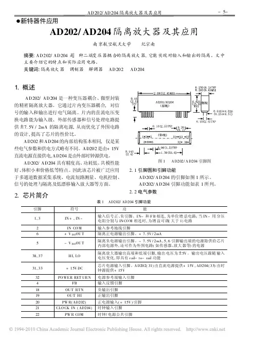
ISO 系列: 直流—电压信号隔离放大器产品特征ISO 系列直流电压信号隔离放大、转换器,是一种将输入的直流电压信号转换成按比例输出的并且与输入信号隔离的直流电流或电压信号的混合集成电路。
产品广泛应用在电力、远程监控、仪器仪表、医疗设备、工业自控等各个需要电量隔离测控的行业。
z 精度等级:0.1级、0.2级、0.5级。
z 0-5V/0-10V/1-5V 等国际标准信号输入,输出标准的隔离信号。
输出电压信号:0-5V/0-10V/1-5V;输出电流信号:0-10mA/0-20mA/4-20mA。
具有高负载能力。
z 全量程范围内极高的线性度(非线性度<2%)型号及定义 通用参数ISO-U□-P□-O□ 精 度---------- 0.1% ,0.2% ,0.5%辅助电源要求---------- DC5V、12V、24V,±10%工作温度---------- -25 ~ +70℃ 工作湿度---------- 10 ~ 90% (无凝露)输入额定电压值 存储温度---------- -45 ~ +85℃U1:0-5V 存储湿度---------- 10 ~ 95% (无凝露) U2:0-10V 隔 离---------- 信号输入/输出/辅助电源 U3:用户自定义 绝缘电阻---------- ≥20MΩ耐 压---------- 信号输入/输出/辅助电源 3KVDC,50Hz,1分钟,漏电流 1mA 耐冲击电压-------- 3KVAC, 1.2/50us(峰值) 辅助电源P1:DC24V P2:DC12V 输入参数 P3:DC5V P4:DC15VP5:用户自定义输出 O1: 4-20mA O2: 0-20mA 输入项目输入阻抗 电源损耗 输入过载能力0-5V 0-10V ≥1M Ω< 0.2W2.0倍额定: 连续 O3: 4-12-20mA O4: 0-5VO5: 0-10V O6: 1-5V O7:用户自定义输出参数输出项目输出过载能力 响应时间4-20mA 产品选型举例例1: 输入:0-5V 辅助电源:24V0-20mA≤350Ω输出: 4-20mA (如果要求负载为650Ω,请另做注明)产品型号: ISO-U1-P1-O1 4-12-20mA例2: 输入:0-10V 辅助电源:12V输出:0-10V 产品型号: ISO-U2-P2-O5注:负载为650Ω时辅助电源的功耗要大一些。

隔离放大器工作原理
隔离放大器是一种特殊的操作放大器,其工作原理是将输入信号隔离开放大器的输出端,以确保输入信号与输出信号之间具有电气隔离,从而实现输入与输出之间的高阻抗隔离。
隔离放大器通常由两个部分组成:输入端和输出端。
输入端接收输入信号,并经过隔离电路进行电气隔离,然后输入到放大器的放大电路中进行放大。
输出端接收来自放大电路的放大信号,并经过隔离电路进行电气隔离,然后输出到负载上。
隔离放大器的工作原理可以通过以下步骤来解释:
1. 输入信号经过输入隔离电路,将输入信号与输出端隔离开,一般使用高阻抗输入电路或光电耦合器实现电气隔离。
2. 经过隔离电路之后,输入信号进入放大电路进行放大。
放大电路可以采用各种不同的放大器电路,如运算放大器、差动放大器等。
3. 放大信号经过输出隔离电路进行电气隔离,一般使用输出变压器、光电耦合器等实现。
4. 经过隔离电路之后,放大信号输出到负载上,并提供给外部设备进行进一步处理。
隔离放大器的主要作用是消除输入与输出之间的电气联系,保证输入信号与输出信号之间的高阻抗隔离,从而避免输入信号对输出信号的影响,同时提高系统的抗干扰能力。
这使得隔离放大器在工业自动化、仪器仪表、医疗设备等领域得到广泛应用。

电路中的隔离放大器有哪些特性隔离放大器是一种常用的电路装置,用于在电气系统中实现信号的隔离和放大。
它具有许多特性,下面将逐一介绍。
一、电气隔离隔离放大器的主要特性之一是电气隔离。
它可以有效地将输入信号隔离开来,防止信号的相互干扰和噪音的干扰。
通过使用隔离放大器,可以将不同电路间的信号完全隔离,确保信号的传递质量和准确性。
二、高精度放大隔离放大器具有高精度放大的特性。
通过精心设计的电路结构和优质的元件,它可以实现对输入信号的高增益放大,同时保持信号的准确性和稳定性。
这使得隔离放大器在测量和控制系统中得到广泛应用,并能够满足高精度要求。
三、广泛的输入输出范围隔离放大器的输入输出范围通常较大。
它可以适应各种输入信号的大小和幅度范围,从微弱的信号到较大的电压信号,都能够实现有效的放大和处理。
这一特性使得隔离放大器适用于不同领域和不同应用环境。
四、低失真隔离放大器具有低失真的特性。
它通过采用高质量的元件和精确的电路设计,可以最大限度地减少信号的失真和失真对输出信号的影响。
这使得隔离放大器能够保持信号的精确度和完整性,同时提供高质量的放大效果。
五、高带宽范围隔离放大器通常具有较高的带宽范围。
这意味着它可以处理高频信号,同时保持信号的准确性和稳定性。
高带宽的特性使得隔离放大器在高速数据传输和信号处理中得到广泛应用,能够满足对信号传输速度要求较高的应用场景。
六、抗干扰能力隔离放大器具有良好的抗干扰能力。
它通过采用屏蔽和隔离技术,可以有效地阻隔外界干扰信号的影响,保持输入信号的纯净性和稳定性。
这使得隔离放大器在复杂电磁环境和强电磁干扰场合下能够正常工作,并保证信号的准确性和可靠性。
综上所述,电路中的隔离放大器拥有电气隔离、高精度放大、广泛的输入输出范围、低失真、高带宽范围和抗干扰能力等特性。
这些特性使得隔离放大器成为电气系统中重要的信号处理装置,广泛应用于工业控制、电力系统、医疗设备等领域,为各种应用场景提供稳定、准确的信号处理和放大功能。
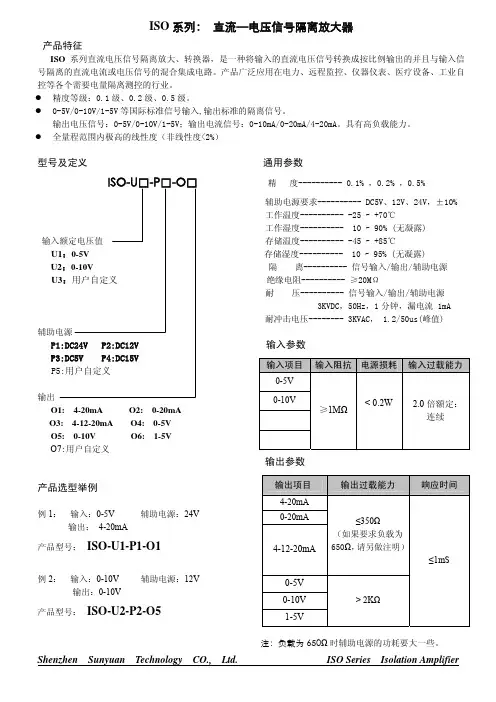
ZB420隔离放大器技术说明书
1、 产品特点
直流电量隔离放大,采用进口芯片,线形度好,隔离强度高; 能对弱电信号4——20mA 电流信号隔离放大; 输入、输出、供电三端隔离,隔离强度高; 模块化封装,方便板上安装; 防尘、抗震、防氧化。
2、技术参数
项 目 单位 最 小 典 型 最 大 测试条件
输入 mA 4 -- 20 输出 VDC 0.8 -- 4.0
输入阻抗 KΩ 100 -- -- 输出负载电阻
KΩ 100 -- -- 精度 ‰ -- 0.2 0.5 温度系数 ppm/℃ -- -- 100
功耗 mA -- -- 100 供电 VDC 4.7 5.0 5.3
输入对电源 100 -- -- 输出对电源 100 -- -- 绝缘强度 (MΩ)
输入对输出 100 -- -- 500V 兆欧表
输入对电源
2000 -- -- 输入对输出 2000 -- -- 介质强度 (VDC) 输出对电源
1000 -- -- 漏电流5mA,1min 无击穿或
闪络
环境温度 ℃ -25 20 70 环境湿度 % -- -- 90 相对湿度
存储温度 ℃ -55 -- +105 存储湿度 % -- -- 95 相对湿度
大气压力 Kpa
80
--
110
安装方式 出针,板上焊接安装,输入为引线。
外型尺寸
33×28×25
2、外型尺寸及出针定义(单位:mm)
针号定义
1 输出+
2 输出-
3 空脚
4 空脚
5 空脚
6 电源输入+
7 电源输入-
红色引线输入+
黑色引线输入-。
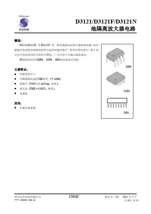
地隔离放大器电路概述:D3121,D3121F 及D3121N 是一块对地能动冲放大器集成电路,该电路能有效消除由线路电阻所引起的问题及噪声。
所需外围电容小,便于设计时小型化的同时可靠性不降低。
广泛应用于车载音响系统内。
D3121系列采用DIP8、SOP8、SIP8的封装形式封装。
主要特点:●外接电容小工●共模抑制比高(57dB 典型,f =1kHz).●低噪声(VNO =3.5mVrms 典型.).●低失真(THD =0.002%典型.).●双通道应用:●车载音响系统DIP8SOP8SIP8内部框图与管脚排列图:D3121/D3121F:D3121N:CHMC极限值(Ta=25︒C)*Reduced by8mW(D3121),4.5mW(D3121F),and9mW(D3121N)for each increase in Ta of1︒C over25︒C 推荐工作条件(Ta=25︒C)电特性:(若无其它规定,Ta=25︒C,Vcc=12V,f=1kHz,Rg=1.8kΩ)CHMCCHMC测试电路图:D3121/D3212F:D3121N:应用图:D3121/D3121F:D3121N:CHMCCHMC应用概要:车载音响系统由于安装于汽车内部,汽车电子所产生的电子噪声可进入功率放大器中,从而产生可听噪声。
车载音响系统噪声流程图D3121利用其一个运算放大器的共模抑制功能来消除噪声,如不使用D3121电路,则噪声直接进入功率放大器;使用时,运算放大器的CMMR 可消除噪声。
噪声消除原理:输出电压获得(eO)理想情况下,如果R1R4=R2R3,and e1=e2,噪声将会变成0。
但是,由于电阻间的失配,噪声电压(e1CHMC与e2)、运算放大器的承受范围会有差别,因而还是会产生噪声电压。
使用注意事项:(1)与pin 2(Vm1)和pin 6(Vm2)相连的电容值比率保持为2:1,则纹波抑抑比稳定,甚至当电容值减半时纹波抑制比仍不会有太大的变动。

精密微型隔离放大器ACPL-C79B/C79A/C790型号:ACPL-C79B/C79A/C790类型:隔离放大器封装:SOP-8电源电压:3 - 5.5VCMR(KV/μs ):15温度范围:-40-105℃隔离能力:5000Vrms品牌:安华高AVAGOACPL-C79B/C79A/C790隔离放大器是专为电机驱动器和可再生能源系统等电子大功率变流器中的电流和电压感测而设计的。
在实施典型的电机驱动程序中,隔离放大器可检测到电机电流通过外部电阻所产生的模拟电压降。
光隔离屏障的另一端则产生差分正比于电机电流的差分输出电压。
建议在通用型应用中采用(±1%增益误差)的ACPL-C79A和(±3%增益误差)的ACPL-C790。
对于高端精密型应用,需采用(±0.5%增益误差)的ACPL-C79B。
该产品采用5V 单电源供电,具备优异的线性度和60 分贝的信噪比动态性能。
由于具有200 kHz 带宽和 1.6µs 的快速响应时间,该产品可以捕获短路和过载情况下的瞬变。
ACPL-C79B/C79A/C790高达(15 kV/µs) 的共模瞬变抑制能力可在高噪声的电机控制环境下精确监测电机电流,其体现的精确性和稳定性足以为各类不同的电机控制应用提供较为平顺的控制(“转矩波动”较小)。
通过结合卓越的光耦技术,ACPL-C79B/C79A/C790 运用Σ-Δ模数转换器技术、斩波稳定放大器以及全差分电路拓朴结构,提供无与伦比的隔离模式噪声抑制能力,降低失调、提高增益,体现精确度和稳定性。
这一性能体现在一个紧凑的自动插入伸展型SO-8 封装产品中,符合世界各地安全法的标准。
ACPL-C79B/C79A/C790特点:0.5% 高增益精度(仅ACPL-C79B)–50 ppm/°C 低增益漂移0.6mV 输入失调电压0.05% 出色的线性度60dB 信噪比200kHz 宽频带宽输出3V 至5.5V 的宽范围电压–40°C 到+105°C 工作温度范围先进的Sigma-Delta (Σ-Δ) 模数转换技术全差分隔离放大器15 kV/µs 共模瞬变抑制能力紧凑的自动插入扩展型SO-8 封装ACPL-C79B/C79A/C790应用:交流与伺服电机驱动的电流/电压检测太阳能逆变器、风力发电机逆变器工业流程控制数据采集系统开关电源信号隔离通用模拟信号隔离取代传统型电流变送器深圳市潮光科技有限公司潮光光耦网: TEL:*************。
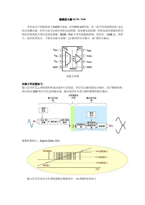
隔离放大器HCPL-7840
安华高生产的隔离放大器HCPL-7840,采用8PIN DIP封装,是一款可用来检测电流/电压的光电耦合器,非常合适马达相位和轨电流检测,逆变器电流检测,传统电流传感器的替代相比传统的霍尔效应电流传感器,HCPL-7840不受外部磁场影响,线性好,CMR高,体积小,成本低等优点。
下图为功能方块图,2,3脚采样信号输入,6,7脚差分输出。
功能方块图
内部工作过程如下:
输入信号经Σ-Δ调制器转换成高速串行比特流,然后经过编码器进行编码,进行模数转换,然后驱动LED将信号传送到输出端,输出端讲信号进行解码数模转换后输出。
模数转换核心:Sigma-Delta调制
输入信号信息包含在调制器输出数据流中,由1和0的密度表示
为了保证良好的线性放大,根据电路中电流的大小可选取合适的分流电阻,使得输入电压范围为-200~+200mV。
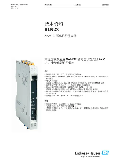
单通道或双通道NAMUR 隔离信号放大器24 V DC,带继电器信号输出应用•隔离信号放大器,用于二进制开关信号的传输•符合NAMUR(EN60947-5-6)的接近传感器输入和开路触点或带电阻性耦合元件的触点•电气3路隔离适合于安全相关应用,满足SIL 2功能安全等级要求,符合IEC 61508标准•选装配备电阻性耦合元件,用于机械开关触点的线路监测•输入回路的线路故障监测,如断路和短路(LFD),可分离通过电源和错误信息模块处的DIN 导轨总线连接头获取组错误信息•输出侧继电器触点作为信号输出,可通过DIP 开关选择动作方向(操作状态或静态电流状态)•应用于–40 … 60 °C (–40 … 140 °F)的环境温度下优势•外壳结构紧凑,宽度仅为:12.5 mm (0.49 in)•有防爆认证,允许选择安装在防爆2区•采用直插式接线端子,快速便捷完成接线;通过DIN 导轨总线连接头选配电源和错误信息模块Products Solutions Services技术资料RLN22NAMUR 隔离信号放大器TI01560K/28/ZH/02.21-00715777272021-10-19RLN222Endress+Hauser目录功能与系统设计 (3)产品描述 ..................................3可靠性....................................3输入 (3)类型......................................3输入数据.. (3)输出.....................................3继电器输出参数..............................3报警信号...................................3防爆连接参数................................4电气隔离...................................4电源.....................................4接线端子分配................................4连接电源...................................4性能参数...................................4接线端子...................................4性能参数 (5)响应时间 (5)安装 (5)安装位置...................................5安装DIN 盘装型设备 (5)环境条件 (5)重要环境条件................................5抗冲击性和抗振性............................5电磁兼容性(EMC) (5)机械结构 (6)设计及外形尺寸..............................6重量......................................6颜色......................................6材质........ (6)显示与操作单元 (7)现场操作...................................7真值表,单通道..............................8真值表,双通道 (8)订购信息..................................8附件.....................................9设备专用附件................................9服务专用附件.. (9)证书和认证 (9)CE 认证....................................9功能安全性.. (10)文档资料 (10)《简明操作指南》(KA)......................10《操作手册》(BA).........................10《安全指南》(XA).........................10补充文档资料...............................10RLN22Endress+Hauser 3功能与系统设计产品描述产品设计NAMUR 隔离放大器,单通道•在订购选项中选择“单通道转换触点”,单通道NAMUR 隔离信号放大器可配备电阻性耦合元件,用于操作接近开关(符合EN 60947-5-6(NAMUR)标准)、断开触点和机械触点。
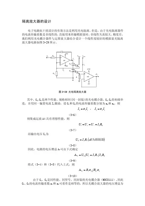
隔离放大器的设计电子电路抗干扰设计的有效方法是利用光电隔离。
但是,由于光电隔离器件的电流传输系数是非线性的,直接用来传输模拟量时,非线性失真较大、精度差,我们利用光电耦合器件与运算放大器结合设计一个线性度较好的模拟量光隔离放大器电路如图3-29所示。
图3-29 光电隔离放大器其中,G 1,G 2是两个性能、规格相同(同一封装)的光电耦合器,G 1,G 2的初级串连,并用同一偏置电流I 1激励,设G 1和G 2的电流传输系数分别为a 2和a 2,则112I I α= , 123I I α=(3-6)则集成运放A4具有理想性能,则62R I U U U i ===-+(3-7)而输出电压U 0为()为跟随器5730A R I U =(3-8)因此,电路的电压增益A V 可由下式确定 627310V A R I R I U U ==(3-9)将式(3-4)和(3-5)代入上式,则 1627V A ααR R =(3-10)由于G 1、G 2是同性能、同型号、同封装的光电耦合器(MOC8111),因此G 1、G 2的电流传输系数a 1和a 2可看作是相等的,所以光耦合放大器的电压增益为67R R A V =(3-11)由此可知,如图所示的光耦放大器增益与G 1,G 2的电流传输系数a 1和a 2无关。
实际上是利用G 1,G 2电流传输系数的对称性补偿了它们之间的非线性。
运放A 5(uA741)接成跟随器形式,以提高电路的负载能力。
运放A 1连接反馈电容C ,用来消除电路的自激振荡。
由于光电耦合器初级、次级之间存在着延迟,使G 1和G 2组成的负反馈电路之间显得迟缓,容易引起电路C 自激振荡,连接电容之后,保证了电路对瞬变信号的负反馈作用,提高了电路的稳定性。
电容C 的容量可根据电路的频率特性要求来确定,经实验和实际应用,电路的非线性误差小于0.2%较好地解决了模拟信号不共地传输的问题。
3.13 可控硅调功控温可控硅调功控温具有不冲击电网,对用电设备不产生干扰等优点,是一种应用广泛的控温方式。

隔离放大器原理
隔离放大器是一种电子器件,用于隔离输入端和输出端之间的电信号,同时放大输入信号的幅度。
它的原理基于电磁感应的原理。
隔离放大器的输入端和输出端之间布置有一个绕组,绕组由一定数量的线圈组成。
当输入信号通过输入端进入绕组时,会在绕组内产生磁场。
这个磁场会通过磁耦合作用影响输出端的绕组。
输出端的绕组内的磁场受到输入信号的影响,从而在绕组上产生与输入信号相对应的电压。
由于输入端和输出端的绕组是电气隔离的,所以输入端和输出端之间的电信号是通过互感耦合实现的,没有直接的电连接。
这样可以有效地隔离输入端和输出端之间的电路,避免干扰信号的传递。
隔离放大器的绕组上还布置有一些其他的电子元件,比如放大器、滤波器等。
这些元件可以增强输入信号的幅度,并对信号进行进一步的处理。
最终,经过隔离放大器处理的信号可以输出到其他设备或电路中。
隔离放大器在许多应用中都有广泛的应用,特别是需要隔离输入信号和输出信号的场合。
比如,在医疗设备中,隔离放大器可以将人体的生理信号转化为可处理的电信号,并确保信号的准确性和安全性。
在工业自动化领域,隔离放大器可以将传感器信号隔离处理,避免干扰和环境噪声的影响。
此外,隔离放大器还可以用于音频信号的隔离放大,以提供更好的音质和音
效。
总结起来,隔离放大器通过互感耦合的原理将输入信号隔离处理,并放大信号的幅度。
它具有电气隔离的特点,可广泛应用于各种领域,为信号处理提供更好的效果。
一种基于隔离放大器的通用直流电压采集电路1.引言1.1 概述概述部分的内容可以按照以下方向进行写作:概述部分旨在引入文章的主题并提供读者必要的背景信息。
在"一种基于隔离放大器的通用直流电压采集电路"这篇文章中,我们将介绍一种利用隔离放大器来实现直流电压采集的电路设计。
直流电压采集在电子领域中非常常见,它广泛应用于工业控制、仪器仪表等领域。
直流电压采集一般需要解决以下问题:首先,直流电压的采集需要高精度,因为直流信号的变化幅度较小;其次,直流电压往往与大地或不同地方的电位参考存在差异,因此需要实现信号的隔离处理,以避免干扰;此外,电路还要考虑输入阻抗、温漂、线性度等因素。
隔离放大器作为一种常见的解决方案,具有信号隔离、电气隔离、增益放大等功能。
它主要由两个部分组成:输入部分和输出部分。
输入部分负责将输入直流电压经过放大后转化为电流信号并隔离,输出部分则将电流信号转化为经过增益放大的输出直流电压。
该技术能够有效解决电气隔离和噪声干扰问题,并提高直流电压采集的精度和稳定性。
在本文中,我们将介绍隔离放大器的原理和作用,并详细讨论通用直流电压采集电路的设计与实现。
通过详细分析电路的关键参数、设计思路和实验结果,读者将能够全面了解该电路的工作原理和特性,以及如何根据具体需求进行设计和优化。
在结论部分,我们将对整篇文章进行总结,并展望该技术在未来的发展方向和应用前景。
本文的目的是为读者提供一种可行的直流电压采集方案,并帮助读者深入理解隔离放大器、直流电压采集电路的原理和设计方法。
希望本文对读者在相关领域的研究和应用有所帮助。
1.2 文章结构文章结构部分的内容可以从以下几个方面展开描述:首先,介绍整篇文章的结构。
可以说明文章从引言、正文到结论的三个主要部分构成,并简要说明每个部分所包含的内容。
其次,具体描述引言部分的内容。
引言部分可以包括概述、文章结构和目的等几个方面。
在概述中,可以简要介绍隔离放大器和通用直流电压采集电路的背景和意义。
隔离放大器原理
隔离放大器是一种电子设备,主要用于将输入信号与输出信号之间进行电气隔离,并通过放大输入信号来得到增强的输出信号。
其工作原理如下:
1. 输入隔离:隔离放大器的第一个功能是将输入信号与输出信号之间进行电气隔离,以防止输入信号中的噪声、电磁干扰等对输出信号产生影响。
这是通过使用隔离变压器和光电隔离器等组件实现的。
输入信号首先被传送到隔离变压器的一侧,而隔离变压器的另一侧与输出信号连接,两者之间没有直接的电气联系。
2. 放大信号:经过输入隔离后的信号被传送到放大器的输入端。
放大器通常采用放大器管或晶体管等放大元件来增大输入信号的幅度。
放大器的放大倍数可以根据需要进行调整,以获得所需的输出信号强度。
3. 输出隔离:经过放大后的信号将被传送到输出隔离器,以实现输出信号与输入信号之间的电气隔离。
输出隔离器通常与输入隔离器使用相同的隔离元件,并将输出信号隔离地传送到输出端口。
隔离放大器的原理在于使用隔离变压器和光电隔离器等元件,将输入信号与输出信号之间进行电气隔离。
这种电气隔离可以有效地阻止输入信号中的噪声、电磁干扰等对输出信号的影响。
同时,通过放大器将输入信号进行放大,可以得到更强的输出
信号。
这种放大过程可以根据需要进行调整,以满足所需的输出信号强度。
1- or 2-channel NAMUR isolating amplifier 24 V DC with relay signal outputApplication•Isolating amplifier for the transmission of binary switch signals•Input for proximity sensors according to NAMUR (EN60947-5-6) and open contacts or contacts with resistive coupling elements •Galvanic 3-way isolationSuitable for safety-oriented applications up to SIL 2 in accordance with IEC61508•Optionally with resistive coupling element for line monitoring of mechanical switching contacts•Monitoring of input circuits for line faults such as breakage and short-circuit (LFD), disengageableGroup error message via DIN rail bus connector at power and error message module•Output-side relay contacts as signal output, direction of action (operating or quiescent current behavior) can be selected via DIP switches •For ambient temperatures –40 to 60 °C (–40 to 140 °F)Your benefits•Compact housing width: 12.5 mm (0.49 in)•Installation in Ex zone 2 permitted in the option with Ex approval•Simple and quick wiring with plug-in terminals, optional power supply and error message via DIN rail bus connectorProducts Solutions ServicesTechnical Information RLN22NAMUR isolating amplifierTI01560K/09/EN/02.21715457402021-10-19RLN222Endress+HauserTable of contentsFunction and system design (3)Product description ............................3Dependability .. (3)Input (3)Version ....................................3Input data . (3)Output (3)Relay output data .............................3Signal on alarm ...............................4Ex connection data ............................4Galvanic isolation .............................4Power supply (4)Terminal assignment ...........................4Connecting the supply voltage .....................4Performance characteristics ......................4Terminals ..................................5Performance characteristics (5)Response time ...............................5Mounting (5)Mounting location .............................5Installing a DIN rail device .. (5)Environment (5)Important ambient conditions .....................5Shock and vibration resistance .....................5Electromagnetic compatibility (EMC). (5)Mechanical construction (6)Design, dimensions ............................6Weight ....................................6Color ......................................6Materials ...................................6Display and operating elements (7)Local operation ...............................7Truth table, 1-channel ..........................8Truth table, 2-channel .. (8)Ordering information ........................8Accessories .. (9)Device-specific accessories .......................9Service-specific accessories .. (9)Certificates and approvals ....................9CE mark ...................................9Functional safety .. (10)Documentation (10)Brief Operating Instructions (KA)..................10Operating Instructions (BA).....................10Safety Instructions (XA)........................10Supplementary device-dependent documentation . (10)RLN22Endress+Hauser 3Function and system designProduct descriptionProduct designNAMUR isolating amplifier 1-channel•With the "1-channel changeover" option, the 1-channel NAMUR isolating amplifier is designed for the operation of proximity switches (as per EN 60947-5-6 (NAMUR)) and open and mechanical contacts with resistive coupling elements. A relay (changeover) is available as the signal output.•The device is optionally available with Ex approvals for the intrinsically safe operation of proximity switches installed in the hazardous area. Separate Ex documentation (XA) is supplied with these devices. Compliance with the installation instructions and connection data in this documentation is mandatory!•A resistive coupling element (1 kΩ / 10 kΩ) is available as an optional accessory and can be used to monitor line faults of sensors with mechanical contacts. The resistive coupling element isinstalled onsite directly at the contact to be monitored or in the sensor connection compartment.NAMUR isolating amplifier 2-channelWith the "2-channel, NO contact" option, the device has a second channel, which is galvanically isolated from channel 1, while maintaining the same width. A relay (NO contact) is available as the signal output. Otherwise, the function corresponds to the 1-channel device.DependabilityWe only provide a warranty if the device is installed and used as described in the Operating Instructions.InputVersionThe following versions are available:•1-channel •2-channelInput data(floating switch contacts with resistive coupling elements to connect NAMUR proximity switches (IEC/EN 60947-5-6))Switch pointsBlocking: < 1.2 mA Conducting: > 2.1 mALine fault detection (response range)Open circuit:0.05 mA < I IN < 0.35 mA Short-circuit:100 Ω < R sensor < 360 ΩShort-circuit current ~ 8 mA Open-circuit voltage~ 8 V DCSwitching hysteresis< 0.2 mAOutputRelay output dataRelay output dataContact design1-channel: 1 changeover 2-channel: 1 NO contact per channelMechanical operating life107 switching cyclesSwitching voltage,maximum switching current250 V DC (2 A) / 120 V DC (0.2 A) / 30 V DC (2 A)Recommended minimum load5 V / 10 mAMaximum switching capacity 500 VASwitching frequency (no load)≤ 20 HzContact materialAgSnO2, hard gold platedDirection of actionOperating current or closed circuit currentRLN224Endress+HauserSignal on alarmOutput behavior in an alarm conditionIf line fault detection is switched on and the line to the sensor is disconnected or short-circuits, the relay de-energizes in such a way that the output is set to the safe, non-conducting state.Line break in input (response range)0.05 mA < I IN < 0.35 mA Monitored range for line breakI IN < 0.05 mALine short circuit in input (response range)100 Ω < R sensor < 360 ΩMonitored range for short circuitR < 100 ΩEx connection data See associated XA Safety InstructionsGalvanic isolationInput / outputPeak value as per EN 60079-11375 VInput / power supply, DIN rail bus connectorPeak value as per EN 60079-11375 VPower supplyTerminal assignmentQuick wiring guide1Terminal assignment of RLN22: 1-channel version (left), 2-channel version (right)Connecting the supply voltagePower can be supplied via terminals 1.1 and 1.2 or via the DIN rail bus connector.Performance characteristicsPower supplySupply voltage range 19.2 to 30 V DC(24 V DC (-20% / +25%))Current consumption at 24 V DC1-channel: ≤ 21 mA 2-channel: ≤ 35 mA Supply current to the DIN rail bus connectorMax. 400 mAPower consumption at 24 V DC1-channel: < 0.65 W 2-channel: < 0.8 W Power loss at 24 V DC1-channel: < 0.65 W 2-channel: < 1 WRLN22Endress+Hauser 5Performance characteristicsResponse timeFollowing a change of state at the input, the output adopts the safe state in ≤ 40 ms.MountingMounting locationThe device is designed for installation on 35 mm (1.38 in) DIN rails in accordance with IEC 60715(TH35).The device's housing provides basic insulation from neighboring devices for 300 Veff. If several devices are installed side by side, this must be taken into consideration and additional insulation must be provided if necessary. If the adjacent device also offers basic insulation, no additional insulation is required.NOTICE‣When using in hazardous areas, the limit values of the certificates and approvals must beobserved.Installing a DIN rail deviceThe device can be installed in any position (horizontal or vertical) on the DIN rail without lateral clearance from neighboring devices. No tools are required for installation. The use of end brackets (type "WEW 35/1" or equivalent) on the DIN rail is recommended to fix the device.EnvironmentImportant ambient conditionsAmbient temperature range–40 to 60 °C (–40 to 140 °F)Storage temperature –40 to 80 °C (–40 to 176 °F)Degree of protection IP 20Overvoltage category IIPollution degree 2Humidity10 to 95 % No condensationAltitude≤ 2 000 m (6 562 ft)Shock and vibration resistance Vibration resistance as per DNVGL-CG-0339 : 2015 and DIN EN 60068-2-27DIN rail device: 2 to 100 Hz at 0.7g (general vibration stress)Shock resistance as per KTA 3505 (section 5.8.4 Shock test)Electromagnetic compatibility (EMC)Interference immunity as per EN 61000-6-2Interference emission as per EN 61000-6-4RLN22Mechanical constructionDesign, dimensions Dimensions in mm (in)Terminal housing for mounting on DIN railWeight Device with terminals (values rounded up):1-channel: approx. 110 g (3.88 oz); 2-channel: approx. 120 g (4.23 oz)Color Light grayMaterials All the materials used are RoHS-compliant.Housing: polycarbonate (PC); flammability rating according to UL94: V-06Endress+HauserRLN22Endress+Hauser 7Display and operating elements2Display and operating elements1Plug-in screw or push-in terminal 2Green LED "On", power supply3Red LED "LF1", line fault of sensor cable 14Red LED "LF2", line fault of sensor cable 2 (option)5Yellow LED "OUT1", status relay 16Yellow LED "OUT2", status relay 2 (option)7DIP switches 1 to 48DIN rail clip for DIN rail mounting 9DIN rail bus connector (optional)Local operation Hardware settings / configurationAny device settings using the DIP switch must be made when the device is de-energized.Direction of actionAt the device, the direction of action (operating or closed circuit current behavior) can be selected and line fault detection can be enabled or disabled via DIP switches.DIP switch 1 = channel 1; DIP switch 3 = channel 2 (optional)All DIP switches are set to the "I" position when the device is delivered from the factory:•I = normal phase (operating current behavior)•II = inverse phase (closed circuit current behavior)Line fault detectionDIP switch 2 = channel 1; DIP switch 4 = channel 2 (optional)I = line fault detection switched off - not permitted for safety-oriented applications!II = line fault detection switched onIf a line fault occurs, the relay is de-energized and the red LED "LF" flashes (NE 44).An error message is transmitted to the power and error message module RNF22 via the DIN rail bus connector and forwarded as a group error message.NOTICEError detection malfunctions‣the "Quick wiring guide" and "Accessories" sections of the Operating Instructions)RLN228Endress+HauserTruth table, 1-channelTruth table, 2-channelOrdering informationDetailed ordering information is available from the nearest sales organization or in the Product Configurator under :1.Select the product using the filters and search field.2.Open the product page.RLN22Endress+Hauser 9The Configurationbutton opens the Product Configurator.Product Configurator - the tool for individual product configuration •Up-to-the-minute configuration data•Depending on the device: Direct input of measuring point-specific information such as measuring range or operating language •Automatic verification of exclusion criteria•Automatic creation of the order code and its breakdown in PDF or Excel output format •Ability to order directly in the Endress+Hauser Online ShopAccessoriesVarious accessories, which can be ordered with the device or subsequently from Endress+Hauser, are available for the device. Detailed information on the order code in question is available from your local Endress+Hauser sales center or on the product page of the Endress+Hauser website: .Device-specific accessoriesService-specific accessoriesCertificates and approvalsFor the approvals available, see the Configurator on the specific product page: → (search for device name)CE markThe product meets the requirements of the harmonized European standards. As such, it complies with the legal specifications of the EC directives. The manufacturer confirms successful testing of the product by affixing to it the CE-mark.RLN2210Endress+HauserFunctional safetyA SIL version of the device is optionally available. It can be used in safety equipment in accordancewith IEC 61508 up to SIL 2 .Please refer to Safety Manual FY01035K for the use of the device in safety instrumentedsystems according to IEC 61508.Protection against modifications:As it is not possible to disengage the operating elements (DIP switches), a lockable control cabinet is required for use in SIL applications. The cabinet must be locked by key. A normal electrical cabinet key does not suffice for this purpose.DocumentationThe following document types are available in the Downloads section of the Endress+Hauser website (/downloads):For an overview of the scope of the associated Technical Documentation, refer to the following:•W@M Device Viewer (/deviceviewer ): Enter the serial number from the nameplate•Endress+Hauser Operations App : Enter the serial number from the nameplate or scan the matrix code on the nameplateBrief Operating Instructions (KA)Guide that takes you quickly to the 1st measured valueThe Brief Operating Instructions contain all the essential information from incoming acceptance to initial commissioning.Operating Instructions (BA)Your reference guideThese Operating Instructions contain all the information that is required in various phases of the life cycle of the device: from product identification, incoming acceptance and storage, to mounting,connection, operation and commissioning through to troubleshooting, maintenance and disposal.Safety Instructions (XA)Depending on the approval, the following Safety Instructions (XA) are supplied with the device. Theyare an integral part of the Operating Instructions.The nameplate indicates the Safety Instructions (XA) that are relevant to the device.Supplementary device-dependent documentationAdditional documents are supplied depending on the device version ordered: Always comply strictly with the instructions in the supplementary documentation. The supplementary documentation is an integral part of the device documentation.*71545740*71545740。