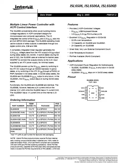
ISL12026
- 格式:pdf
- 大小:389.09 KB
- 文档页数:24
®ISL12026, ISL12026AReal Time Clock/Calendar with I 2C Bus™ and EEPROMThe ISL12026 and the ISL12026A devices are micro power real time clocks with timing and crystal compensation, clock/calender, power-fail indicator, two periodic or polled alarms, intelligent battery backup switching, and integrated 512x8-bit EEPROM configured in 16 Bytes per page.The oscillator uses an external, low-cost 32.768kHz crystal. The real time clock tracks time with separate registers for hours, minutes, and seconds. The device has calendar registers for date, month, year and day of the week. The calendar is accurate through 2099, with automatic leap year correction.The ISL12026 and ISL12026A have different types of Power Control Settings. The ISL12026 uses the Legacy ModeSetting, which follows conditions set in X1226 products. The ISL12026A uses the Standard Mode Setting. Please refer to “Power Control Operation” on page 13 for more details. Also, please refer to “I 2C Communications During Battery Backup” on page 22 for important details.PinoutsISL12026, ISL12026A(8 LD SOIC)TOP VIEWISL12026, ISL12026A(8 LD TSSOP)TOP VIEWFeatures•Real Time Clock/Calendar-Tracks Time in Hours, Minutes and Seconds -Day of the Week, Day, Month and Year - 3 Selectable Frequency Outputs•Two Non-Volatile Alarms-Settable on the Second, Minute, Hour, Day of the Week, Day or Month-Repeat Mode (Periodic Interrupts)•Automatic Backup to Battery or SuperCap•On-Chip Oscillator Compensation-Internal Feedback Resistor and Compensation Capacitors-64 Position Digitally Controlled Trim Capacitor- 6 Digital Frequency Adjustment Settings to ±30ppm •512x8 Bits of EEPROM-16-Byte Page Write Mode (32 total pages)-8 Modes of BlockLock™ Protection -Single Byte Write Capability•High Reliability-Data Retention: 50 years-Endurance: >2,000,000 Cycles Per Byte•I 2C Interface-400kHz Data Transfer Rate •800nA Battery Supply Current•Package Options-8 Ld SOIC and 8 Ld TSSOP Packages •Pb-Free (RoHS Compliant)Applications•Utility Meters •HVAC Equipment•Audio/Video Components •Set-Top Box/Television •Modems•Network Routers, Hubs, Switches, Bridges •Cellular Infrastructure Equipment•Fixed Broadband Wireless Equipment •Pagers/PDA •POS Equipment •Test Meters/Fixtures•Office Automation (Copiers, Fax)•Home Appliances •Computer Products•Other Industrial/Medical/AutomotiveX1X2V BAT V DD IRQ/F OUTSCL SDAGND12347865X1X2V BAT V DD IRQ/F OUTSCL SDA GND 12347865Block DiagramOrdering InformationPART NUMBER(Note)PART MARKING V BAT TRIP POINT(V)BSW BIT DEFAULT SETTING TEMP RANGE(°C)PACKAGE(Pb-Free)PKG. DWG. #ISL12026IBZ*12026 IBZ V DD < V BAT BSW = 1-40 to +858 Ld SOIC M8.15ISL12026IVZ*2026 IVZ V DD < V BATBSW = 1-40 to +858 Ld TSSOP M8.173ISL12026AIBZ*12026A IBZ 2.2BSW = 0-40 to +858 Ld SOIC M8.15ISL12026AIVZ*12026A IVZ2.2BSW = 0-40 to +858 Ld TSSOPM8.173*Add “-T” suffix for tape and reel. Please refer to TB347 for details on reel specifications.NOTE:These Intersil Pb-free plastic packaged products employ special Pb-free material sets, molding compounds/die attach materials, and 100% matte tin plate plus anneal (e3 termination finish, which is RoHS compliant and compatible with both SnPb and Pb-free soldering operations). Intersil Pb-free products are MSL classified at Pb-free peak reflow temperatures that meet or exceed the Pb-free requirements of IPC/JEDEC J STD-020.X1X2OSCILLATORFREQUENCY TIMER LOGICDIVIDERCALENDAR 8CONTROL/REGISTERS 1HzTIME KEEPING REGISTERS ALARM REGS COMPARE M A S KCONTROL DECODE LOGICALARM(EEPROM)(EEPROM)SCL SDASERIAL INTERFACE DECODER4k EEPROM ARRAYREGISTERS STATUS (SRAM)SELECTIRQ/F OUTV DD V BAT32.768kHz (SRAM)BATTERY CIRCUITRYSWITCH OSCCOMPENSATIONPin DescriptionsPIN NUMBER SYMBOLDESCRIPTIONSOIC TSSOP 13X1The X1 pin is the input of an inverting amplifier and is intended to be connected to one pin of an external 32.768kHz quartz crystal. X1 can also be driven directly from a 32.768kHz source (see “Application Section” on page 19.)24X2The X2 pin is the output of an inverting amplifier and is intended to be connected to one pin of an external 32.768kHz quartz crystal (see “Application Section” on page 19.)35IRQ/F OUT Interrupt Output/Frequency Output is a multi-functional pin that can be used as interrupt or frequency output pin. The function is set via the control register. This output is an open drain configuration.46GND Ground.57SDA Serial Data (SDA) is a bidirectional pin used to transfer serial data into and out of the device. It has an open drain output and may be wire OR’ed with other open drain or open collector outputs.68SCL The Serial Clock (SCL) input is used to clock all serial data into and out of the device. The input buffer on this pin is always active (not gated).71V BAT This input provides a backup supply voltage to the device. V BAT supplies power to the device in the event that the V DD supply fails. This pin should be tied to ground if not used.82V DDPower Supply.Absolute Maximum Ratings Thermal InformationVoltage on V DD, V BAT, SCL, SDA, and IRQ/F OUT Pins(respect to ground). . . . . . . . . . . . . . . . . . . . . . . . . . -0.3V to 6.0V Voltage on X1 and X2 Pins(respect to ground). . . . . . . . . . . . . . . . . . . . . . . . . . -0.3V to 2.5V Latchup (Note 1) . . . . . . . . . . . . . . . . . . .Class II, Level B @ +85°C ESD RatingHuman Body Model . . . . . . . . . . . . . . . . . . . . . . . . . . . . . . . .±2kV Machine Model. . . . . . . . . . . . . . . . . . . . . . . . . . . . . . . . . . . .175V Thermal Resistance (Typical, Note 2)θJA (°C/W) 8 Ld SOIC Package. . . . . . . . . . . . . . . . . . . . . . . . . 1208 Ld TSSOP Package . . . . . . . . . . . . . . . . . . . . . . . 140 Storage Temperature. . . . . . . . . . . . . . . . . . . . . . . .-65°C to +150°C Pb-free reflow profile . . . . . . . . . . . . . . . . . . . . . . . . . .see link below /pbfree/Pb-FreeReflow.aspCAUTION: Do not operate at or near the maximum ratings listed for extended periods of time. Exposure to such conditions may adversely impact product reliability and result in failures not covered by warranty.NOTES:1.Jedec Class II pulse conditions and failure criterion used. Level B exceptions are: Using a max positive pulse of 8.35V on all pins except X1 andX2, Using a max positive pulse of 2.75V on X1 and X2, and using a max negative pulse of -1V for all pins.2.θJA is measured with the component mounted on a high effective thermal conductivity test board in free air. See Tech Brief TB379 for details.DC Electrical Specifications Unless otherwise noted, V DD = +2.7V to +5.5V, T A = -40°C to +85°C, Typical values are @ T A = +25°Cand V DD = 3.3V.SYMBOL PARAMETER CONDITIONSMIN(Note 12)TYPMAX(Note 12)UNIT NOTESV DD Main Power Supply 2.7 5.5V V BAT Backup Power Supply 1.8 5.5V Electrical SpecificationsSYMBOL PARAMETER CONDITIONSMIN(Note 12)TYPMAX(Note 12)UNIT NOTESI DD1Supply Current with I2C Active V DD = 2.7V500µA3, 4, 5V DD = 5.5V800µAI DD2Supply Current for Non-VolatileProgramming V DD = 2.7V 2.5mA3, 4, 5 V DD = 5.5V 3.5mAI DD3Supply Current for MainTimekeeping (Low Power Mode)V DD = V SDA = V SCL = 2.7V10µA5 V DD = V SDA = V SCL = 5.5V20µAI BAT Battery Supply Current V BAT = 1.8V,V DD = V SDA = V SCL = V RESET = 08001000nA3, 6, 7V BAT = 3.0V,V DD = V SDA = V SCL = V RESET = 08501200nAI BATLKG Battery Input Leakage V DD = 5.5V, V BAT = 1.8V100nAV TRIP V BAT Mode Threshold 1.8 2.2 2.6V7V TRIPHYS V TRIP Hysteresis30mV7, 10, 13 V BATHYS V BAT Hysteresis50mV7, 10, 13 V DD SR-V DD Negative Slew Rate10V/ms8 IRQ/F OUTV OL Output Low Voltage V DD = 5VI OL = 3mA0.4VV DD = 1.8VI OL = 1mA0.4VI LO Output Leakage Current V DD = 5.5VV OUT = 5.5V100400nAEEPROM SpecificationsPARAMETER TEST CONDITIONSMIN(Note 12)TYPMAX(Note 12)UNITS NOTESEEPROM Endurance>2,000,000Cycles EEPROM Retention Temperature ≤ +75°C50YearsSerial Interface (I2C) SpecificationsDC Electrical SpecificationsSYMBOL PARAMETER TEST CONDITIONSMIN(Note 12)TYPMAX(Note 12)UNITS NOTESV IL SDA and SCL Input Buffer LOWVoltage-0.30.3xV DD VV IH SDA and SCL Input Buffer HIGHVoltage0.7 x V DD V DD + 0.3VHysteresis SDA and SCL Input BufferHysteresis0.05 x V DD V13V OL SDA Output Buffer LOW Voltage I OL = 4mA00.4VI LI Input Leakage Current on SCL V IN = 5.5V100nAI LO I/O Leakage Current on SDA V IN = 5.5V100nAAC Electrical SpecificationsSYMBOL PARAMETER TEST CONDITIONSMIN(Note 12)TYPMAX(Note 12)UNITS NOTESf SCL SCL Frequency400kHzt IN Pulse width Suppression Time at SDA and SCL Inputs Any pulse narrower than the maxspec is suppressed.50nst AA SCL Falling Edge to SDA Output Data Valid SCL falling edge crossing 30% ofV DD, until SDA exits the 30% to 70%of V DD window.900nst BUF Time the Bus Must be Free Before the Start of a New Transmission SDA crossing 70% of V DD during aSTOP condition, to SDA crossing70% of V DD during the followingSTART condition.1300nst LOW Clock LOW Time Measured at the 30% of V DDcrossing.1300nst HIGH Clock HIGH Time Measured at the 70% of V DDcrossing.600nst SU:STA START Condition Set-up Time SCL rising edge to SDA falling edge.Both crossing 70% of V DD.600nst HD:STA START Condition Hold Time From SDA falling edge crossing30% of V DD to SCL falling edgecrossing 70% of V DD.600nst SU:DAT Input Data Set-up Time From SDA exiting the 30% to 70% ofV DD window, to SCL rising edgecrossing 30% of V DD.100nst HD:DAT Input Data Hold Time From SCL rising edge crossing 70%of V DD to SDA entering the 30% to70% of V DD window.0nsTiming DiagramsBus Timingt SU:STOSTOP Condition Set-up TimeFrom SCL rising edge crossing 70% of V DD , to SDA rising edge crossing 30% of V DD .600nst HD:STO STOP Condition Hold Time for Read or Volatile Only Write From SDA rising edge to SCL falling edge. Both crossing 70% of V DD .600ns t DHOutput Data Hold TimeFrom SCL falling edge crossing 30% of V DD , until SDA enters the 30% to 70% of V DD window.nsCpin SDA and SCL Pin Capacitance 10pF 13t WC Non-volatile Write Cycle Time 1220ms 10t R SDA and SCL Rise Time From 30% to 70% of V DD 20 + 0.1xCb 300ns 11, 13t F SDA and SCL Fall TimeFrom 70% to 30% of V DD20 +0.1xCb300ns 11, 13Cb Capacitive Loading of SDA or SCL Total on-chip and off-chip10400pF 11, 13R PUSDA and SCL Bus Pull-up Resistor Off-chip Maximum is determined by t R and t F . For Cb = 400pF, max is about2k Ω~2.5k Ω.For Cb = 40pF, max is about 15k Ω~20k Ω1k Ω11, 13NOTES:3.IRQ/F OUT Inactive.4.V IL = V DD x 0.1, V IH = V DD x 0.9, f SCL = 400kHz5.V DD > V BAT +V BATHYS6.Bit BSW = 0 (Standard Mode), ATR = 00h, V BAT ≥1.8V7.Specified at +25°C.8.In order to ensure proper timekeeping, the V DD SR- specification must be followed.9.Parameter is not 100% tested.10.t WC is the minimum cycle time to be allowed for any non-volatile Write by the user, it is the time from valid STOP condition at the end of Writesequence of a serial interface Write operation, to the end of the self-timed internal non-volatile write cycle.11.These are I 2C specific parameters and are not directly tested, however they are used during device testing to validate device specification.12.Parameters with MIN and/or MAX limits are 100% tested at +25°C, unless otherwise specified. Temperature limits established bycharacterization and are not production tested.13.Limits should be considered typical and are not production tested.AC Electrical Specifications(Continued)SYMBOL PARAMETERTEST CONDITIONSMIN (Note 12)TYPMAX (Note 12)UNITS NOTESt SDA(OUTPUT TIMING)t t tWrite Cycle TimingSCLSDASTOP CONDITIONSTART CONDITIONTypical Performance Curves Temperature is +25°C unless otherwise specified.FIGURE 1.I BAT vs V BAT, SBIB = 0FIGURE 2.I BAT vs V BAT, SBIB = 1FIGURE 3.I DD3 vs TEMPERATUREFIGURE 4.I BAT vs TEMPERATURE0.00.51.01.52.02.53.03.54.01.82.32.83.33.84.34.85.3V BAT (V)I B A T (µA )SCL, SDA PULL-UPS = 0VSCL, SDA PULL-UPS = V BATBSW = 0 OR 1BSW = 0 OR 10.00.10.20.30.40.50.60.70.80.91.82.32.83.33.84.34.85.3V BAT (V)I B A T (µA )SCL, SDA PULL-UPS = 0VBSW = 0 OR 10.00.51.01.52.02.53.03.54.04.55.0-45-35-25-15-551525354555657585TEMPERATURE (°C)I D D (µA )V DD = 3.3VV DD = 5.5V0.00.20.40.60.81.01.21.4-45-35-25-15-551525354555657585TEMPERATURE (°C)I B A T (µA )V BAT = 3.0VDescriptionThe ISL12026 device is a Real Time Clock with clock/calendar, two polled alarms with integrated 512x8 EEPROM, oscillator compensation and battery backup switch. The oscillator uses an external, low-cost 32.768kHz crystal. All compensation and trim components are integrated on the chip. This eliminates several external discrete components and a trim capacitor, saving board area and component cost.The Real Time Clock keeps track of time with separateregisters for Hours, Minutes and Seconds. The Calendar has separate registers for Date, Month, Year and Day-of-week. The calendar is correct through 2099, with automatic leap year correction.The Dual Alarms can be set to any Clock/Calendar value for a match. For instance, every minute, every Tuesday, or 5:23 AM on March 21. The alarms can be polled in the Status Register or can provide a hardware interrupt (IRQ/F OUT Pin). There is a pulse mode for the alarms allowing for repetitive alarm functionality.The IRQ/F OUT pin may be software selected to provide a frequency output of 1Hz, 4096Hz, or 32,768Hz or inactive. The device offers a backup power input pin. This V BAT pin allows the device to be backed up by battery or SuperCap. The entire ISL12026 device is fully operational from 2.7V to 5.5V and the clock/calendar portion of the ISL12026 device remains fully operational down to 1.8V (Standby Mode).The ISL12026 device provides 4k bits of EEPROM with 8 modes of BlockLock™ control. The BlockLock™ allows a safe, secure memory for critical user and configuration data, while allowing a large user storage area.Pin DescriptionsSerial Clock (SCL)The SCL input is used to clock all data into and out of the device. The input buffer on this pin is always active (not gated). The pull-up resistor on this pin must use the same voltage source as V DD .Serial Data (SDA)SDA is a bidirectional pin used to transfer data into and out of the device. It has an open drain output and may be wire ORed with other open drain or open collector outputs. The input buffer is always active (not gated).This open drain output requires the use of a pull-up resistor. The pull-up resistor on this pin must use the same voltage source as V DD . The output circuitry controls the fall time of the output signal with the use of a slope controlled pull-down. The circuit is designed to comply with 400kHz I 2C interface speed.V BATThis input provides a backup supply voltage to the device. V BAT supplies power to the device in the event the V DD supply fails. This pin can be connected to a battery, a SuperCap or tied to ground if not used.IRQ/F OUT (Interrupt Output/Frequency Output)This dual function pin can be used as an interrupt orfrequency output pin. The IRQ/F OUT mode is selected via the frequency out control bits of the INT register.•Interrupt Mode. The pin provides an interrupt signaloutput. This signal notifies a host processor that an alarm has occurred and requests action. It is an open drain active low output.•Frequency Output Mode. The pin outputs a clock signal which is related to the crystal frequency. The frequency output is user selectable and enabled via the I 2C bus. It is an open drain output.FIGURE 5.I DD3 vs V DD FIGURE 6.ΔF OUT vs ATR SETTINGTypical Performance Curves (Continued)Temperature is +25°C unless otherwise specified.0.00.51.01.52.02.53.03.54.04.51.82.32.83.33.84.34.85.3V DD (V)I D D (µA )-40-20020406080-32-28-24-20-16-12-8-40481216202428ATR SETTINGP P M C H A N G E F R O M A T R = 0X1, X2The X1 and X2 pins are the input and output, respectively, of an inverting amplifier. An external 32.768kHz quartz crystal is used with the ISL12026 to supply a timebase for the real time clock. Internal compensation circuitry provides high accuracy over the operating temperature range from-40°C to +85°C. This oscillator compensation network can be used to calibrate the crystal timing accuracyover-temperature either during manufacturing or with an external temperature sensor and microcontroller for active compensation. X2 is intended to drive a crystal only, and should not drive any external circuit.Real Time Clock OperationThe Real Time Clock (RTC) uses an external 32.768kHz quartz crystal to maintain an accurate internal representation of the second, minute, hour, day, date, month and year. The RTC has leap-year correction. The clock also corrects for months having fewer than 31 days and has a bit that controls 24 hour or AM/PM format. When the ISL12026 powers up after the loss of both V DD and V BAT, the clock will not operate until at least one byte is written to the clock register.Reading the Real Time ClockThe RTC is read by initiating a Read command and specifying the address corresponding to the register of the Real Time Clock. The RTC Registers can then be read in a Sequential Read Mode. Since the clock runs continuously and a read takes a finite amount of time, there is the possibility that the clock could change during the course of a read operation. In this device, the time is latched by the read command (falling edge of the clock on the ACK bit prior to RTC data output) into a separate latch to avoid time changes during the read operation. The clock continues to run. Alarms occurring during a read are unaffected by the read operation.Writing to the Real Time ClockThe time and date may be set by writing to the RTC registers. RTC Register should be written ONLY with Page Write. To avoid changing the current time by an incomplete write operation, write to the all 8 bytes in one write operation. When writing the RTC registers, the new time value is loaded into a separate buffer at the falling edge of the clock during the Acknowledge. This new RTC value is loaded into the RTC Register by a stop bit at the end of a valid write sequence. An invalid write operation aborts the time update procedure and the contents of the buffer are discarded. After a valid write operation, the RTC will reflect the newly loaded data beginning with the next “one second” clock cycle after the stop bit is written. The RTC continues to update the time while an RTC register write is in progress and the RTC continues to run during any non-volatile write sequences.Accuracy of the Real Time ClockThe accuracy of the Real Time Clock depends on the accuracy of the quartz crystal that is used as the time base for the RTC. Since the resonant frequency of a crystal is temperature dependent, the RTC performance will also be dependent upon temperature. The frequency deviation of the crystal is a function of the turnover temperature of the crystal from the crystal’s nominal frequency. For example, a >20ppm frequency deviation translates into an accuracy of >1 minute per month. These parameters are available from the crystal manufacturer. Intersil’s RTC family provideson-chip crystal compensation networks to adjustload-capacitance to tune oscillator frequency from -34ppm to +80ppm when using a 12.5pF load crystal. For more detailed information, see “Application Section” on page19.Clock/Control Registers (CCR)The Control/Clock Registers are located in an area separate from the EEPROM array and are only accessible following a slave byte of “1101111x” and reads or writes to addresses [0000h:003Fh]. The clock/control memory map has memory addresses from 0000h to 003Fh. The defined addresses are described in the Table 1. Writing to and reading from the undefined addresses are not recommended.CCR AccessThe contents of the CCR can be modified by performing a byte or a page write operation directly to any address in the CCR. Prior to writing to the CCR (except the status register), however, the WEL and RWEL bits must be set using a three step process (see “Writing to the Clock/Control Registers” on page12).The CCR is divided into 5 sections. These are:1.Alarm 0 (8 bytes; non-volatile)2.Alarm 1 (8 bytes; non-volatile)3.Control (5 bytes; non-volatile)4.Real Time Clock (8 bytes; volatile)5.Status (1 byte; volatile)Each register is read and written through buffers. Thenon-volatile portion (or the counter portion of the RTC) is updated only if RWEL is set and only after a valid write operation and stop bit. A sequential read or page write operation provides access to the contents of only one section of the CCR per operation. Access to another section requires a new operation. A read or write can begin at any address in the CCR.It is not necessary to set the RWEL bit prior to writing the status register. See “Status Register (SR)” on page9. supports a single byte read or write only. Continued reads or writes from this section terminates the operation.X1X2FIGURE 7.RECOMMENDED CRYSTAL CONNECTIONThe state of the CCR can be read by performing a random read at any address in the CCR at any time. This returns the contents of that register location. Additional registers are read by performing a sequential read. The read instruction latches all Clock registers into a buffer, so an update of the clock does not change the time being read. A sequential read of the CCR will not result in the output of data from the memory array. At the end of a read, the master supplies a stop condition to end the operation and free the bus. After a read of the CCR, the address remains at the previous address +1 so the user can execute a current address read of the CCR and continue reading the next Register.Real Time Clock RegistersSC, MN, HR, DT, MO, YR: Clock/Calendar Registers These registers depict BCD representations of the time. As such, SC (Seconds) and MN (Minutes) range from 00 to 59, HR (Hour) is 1 to 12 with an AM or PM indicator (H21 bit) or 0 to 23 (with MIL = 1), DT (Date) is 1 to 31, MO (Month) is 1 to 12, YR (Year) is 0 to 99.DW: Day of the Week RegisterThis register provides a Day of the Week status and uses three bits DY2 to DY0 to represent the seven days of the week. The counter advances in the cycle 0-1-2-3-4-5-6-0-1-2-… The assignment of a numerical value to a specific day of the week is arbitrary and may be decided by the system software designer. The default value is defined as ‘0’.24 Hour TimeIf the MIL bit of the HR register is 1, the RTC uses a 24-hour format. If the MIL bit is 0, the RTC uses a 12-hour format and H21 bit functions as an AM/PM indicator with a ‘1’ representing PM. The clock defaults to standard time with H21 = 0.Leap YearsLeap years add the day February 29 and are defined as those years that are divisible by 4.Status Register (SR)The Status Register is located in the CCR memory map at address 003Fh. This is a volatile register only and is used to control the WEL and RWEL write enable latches, read power status and two alarm bits. This register is separate from both the array and the Clock/Control Registers (CCR).BAT: Battery Supply - VolatileThis bit set to “1” indicates that the device is operating from V BAT, not V DD. It is a read-only bit and is set/reset by hardware (ISL12026 internally). Once the device begins operating from V DD, the device sets this bit to “0”.AL1, AL0: Alarm Bits - VolatileThese bits announce if either alarm 0 or alarm 1 match the real time clock. If there is a match, the respective bit is set to ‘1’. The falling edge of the last data bit in a SR Read operation resets the flags. Note: Only the AL bits that are set when an SR read starts will be reset. An alarm bit that is set by an alarm occurring during an SR read operation will remain set after the read operation is complete.OSCF: Oscillator Fail IndicatorThis bit is set to “1” if the oscillator is not operating, or is operating, but has clock jitter which does not affect the accuracy of RTC counting. The bit is set to “0” if the oscillator is functioning, and does not have clock jitter. This bit is read only, and is set/reset by hardware.RWEL: Register Write Enable Latch - VolatileThis bit is a volatile latch that powers up in the LOW (disabled) state. The RWEL bit must be set to “1” prior to any writes to the Clock/Control Registers. Writes to RWEL bit do not cause a non-volatile write cycle, so the device is ready for the next operation immediately after the stop condition. A write to the CCR requires both the RWEL and WEL bits to be set in a specific sequence.WEL: Write Enable Latch - VolatileThe WEL bit controls the access to the CCR during a write operation. This bit is a volatile latch that powers up in the LOW (disabled) state. While the WEL bit is LOW, writes to the CCR address will be ignored, although acknowledgment is still issued. The WEL bit is set by writing a “1” to the WEL bit and zeroes to the other bits of the Status Register. Once set, WEL remains set until either reset to 0 (by writing a “0” to the WEL bit and zeroes to the other bits of the Status Register) or until the part powers up again. Writes to WEL bit do not cause a non-volatile write cycle, so the device is ready for the next operation immediately after the stop condition.RTCF: Real Time Clock Fail Bit - VolatileThis bit is set to a “1” after a total power failure. This is a read only bit that is set by hardware (ISL12026 internally) when the device powers up after having lost all power to the device (both V DD and V BAT go to 0V). The bit is set regardless of whether V DD or V BAT is applied first. The loss of only one of the supplies does not set the RTCF bit to “1”. On power-up after a total power failure, all registers are set to their default states and the clock will not increment until at least one byte is written to the clock register. The first valid write to the RTC section after a complete power failure resets the RTCF bit to “0” (writing one byte is sufficient).Unused BitsBit 3 in the SR is not used, but must be zero. The Data Byte output during a SR read will contain a zero in this bit location.TABLE 1.STATUS REGISTER (SR)ADDR76543210 003Fh BAT AL1AL0OSCF0RWEL WEL RTCF Default00000001Alarm Registers (Non-Volatile)Alarm0 and Alarm1The alarm register bytes are set up identical to the RTC register bytes, except that the MSB of each byte functions as an enable bit (enable = “1”). These enable bits specify which alarm registers (seconds, minutes, etc.) are used to make the comparison. Note that there is no alarm byte for year.The alarm function works as a comparison between the alarm registers and the RTC registers. As the RTC advances, the alarm will be triggered once a match occurs between the alarm registers and the RTC registers. Any one alarm register, multiple registers, or all registers can be enabled for a match. See “Device Operation” on page12 and “Application Section” on page19 for more information.Control Registers (Non-Volatile)The Control Bits and Registers described in the following are non-volatile.BL RegisterBP2, BP1, BP0 - Block Protect BitsThe Block Protect Bits, BP2, BP1 and BP0, determine which blocks of the array are write protected. A write to a protected block of memory is ignored. The block protect bits will prevent write operations to one of eight segments of the array. The partitions are described in T able 3.TABLE 2.CLOCK/CONTROL MEMORY MAPADDR.TYPE REG NAMEBITRANGE I SL1226DEFAULTISL1226ADEFAULT 76543210003F Status SR BAT AL1AL0OSCF0RWEL WEL RTCF01h01h0037RTC(SRAM)Y2K00Y2K21Y2K20Y2K1300Y2K1019/2020h20h0036DW00000DY2DY1DY00-600h00h 0035YR Y23Y22Y21Y20Y13Y12Y11Y100-9900h00h 0034MO000G20G13G12G11G101-1200h00h 0033DT00D21D20D13D12D11D101-3101h01h 0032HR MIL0H21H20H13H12H11H100-2300h00h 0031MN0M22M21M20M13M12M11M100-5900h00h 0030SC0S22S21S20S13S12S11S100-5900h00h0014Control(EEPROM)PWR SBIB BSW00000040h00h0013DTR00000DTR2DTR1DTR000h00h 0012ATR00ATR5ATR4ATR3ATR2ATR1ATR000h00h 0011INT IM AL1E AL0E FO1FO000000h00h 0010BL BP2BP1BP00000000h00h000F Alarm1(EEPROM)Y2K100A1Y2K21A1Y2K20A1Y2K1300A1Y2K1019/2020h20h000E DWA1EDW10000DY2DY1DY00-600h00h 000D YRA1Unused - Default = RTC Year value (No EEPROM) - Future expansion000C MOA1EMO100A1G20A1G13A1G12A1G11A1G101-1200h00h 000B DTA1EDT10A1D21A1D20A1D13A1D12A1D11A1D101-3100h00h 000A HRA1EHR10A1H21A1H20A1H13A1H12A1H11A1H100-2300h00h 0009MNA1EMN1A1M22A1M21A1M20A1M13A1M12A1M11A1M100-5900h00h 0008SCA1ESC1A1S22A1S21A1S20A1S13A1S12A1S11A1S100-5900h00h0007Alarm0(EEPROM)Y2K000A0Y2K21A0Y2K20A0Y2K1300A0Y2K1019/2020h20h0006DWA0EDW00000DY2DY1DY00-600h00h 0005YRA0Unused - Default = RTC Year value (No EEPROM) - Future expansion0004MOA0EMO000A0G20A0G13A0G12A0G11A0G101-1200h00h 0003DTA0EDT00A0D21A0D20A0D13A0D12A0D11A0D101-3100h00h 0002HRA0EHR00A0H21A0H20A0H13A0H12A0H11A0H100-2300h00h 0001MNA0EMN0A0M22A0M21A0M20A0M13A0M12A0M11A0M100-5900h00h 0000SCA0ESC0A0S22A0S21A0S20A0S13A0S12A0S11A0S100-5900h00h。