HMD1M32M2EG-7中文资料
- 格式:pdf
- 大小:72.93 KB
- 文档页数:7
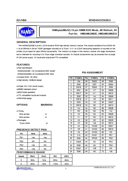
HANBit HMD1M32M2EGPIN ASSIGNMENTDESCRIPTIONThe HMD1M32M2EG is an 1M x 32 bits Dynamic RAM MODULE which is assembled 2 pieces of 1M x 16bit DRAMs in 42 pin SOJ package on single sides the printed circuit board with decoupling capacitors. The HMD1M32M2EG is optimized for application to the systems, which are required high density and large capacity such as main memory of the computers and an image memory systems, and to the others, which are, requested compact size. The HMD1M32M2G provides common data and outputs.Featuresw Part Indentification -HMD1M32M2EG – Gold plate Lead w 72 pins Single In-Line Package w EDO Mode Capabilityw Single +5V ± 0.5V power supply w Fast Access Time & Cycle TimeT RAC t CAC t RC t HPC HMD1M32M2EG-45 45 13 69 16 HMD1M32M2EG-50 50 15 84 20 HMD1M32M2EG-60 601710425w Low PowerActive: 1,870/1,650/1,430 mW(MAX) Standby: 11mW(CMOS level : MAX)w /RAS Only Refresh, /CAS before /RAS Refresh, Hidden Refresh Capabilityw All inputs and outputs TTL Compatible w 1,024 Refresh Cycles/16msPIN DESCRIPTIONPin FUNCTIONPIN FUNCTIONA0 – A9 Address Inputs PD1 – PD4Presence Detect DQ0 – DQ31 Data Input/Output Vcc Power (+5V) /RAS0, /RAS2 Row Address Strobe Vss Ground /CAS0 - /CAS3Column Address Strobe NC No Connection /WERead/Write Enable--PIN SYMBOL PINSYMBOL PIN SYMBOL 1 Vss 25 DQ22 49 DQ8 2 DQ0 26 DQ7 50 DQ24 3 DQ16 27 DQ23 51 DQ9 4 DQ1 28 A7 52 DQ25 5 DQ17 29 NC 53 DQ10 6 DQ2 30 Vcc 54 DQ26 7 DQ18 31 A8 55 DQ11 8 DQ3 32 A9 56 DQ27 9 DQ19 33 NC 57 DQ12 10 Vcc 34 /RAS2 58 DQ28 11 NC 35 NC 59 Vcc 12 A0 36 NC 60 DQ29 13 A1 37 NC 61 DQ13 14 A2 38 NC 62 DQ30 15 A3 39 Vss 63 DQ14 16 A4 40 /CAS0 64 DQ31 17 A5 41 /CAS2 65 DQ15 18 A6 42 /CAS3 66 NC 19 NC 43 /CAS1 67 PD1 20 DQ4 44 /RAS0 68 PD2 21 DQ20 45 NC 69 PD3 22 DQ5 46 NC 70 PD4 23 DQ21 47 /WE 71 NC 24DQ6 48NC72 VssHANBit HMD1M32M2EGFUNCTIONAL BLOCK DIAGRAM/RAS0/CAS0/CAS1 /RAS2/CAS2/CAS3/WE A0-A9U0-U1U0-U1 1Mx16 DRAM U0-U1DQ0-DQ7DQ8-DQ15DQ16-DQ23DQ24-DQ31*NOTE: 1. Stress greater than above absolute Maximum Ratings? May cause permanent damage to the device. RECOMMENDED DC OPERATING CONDITIONS (TA = 0 ~ 70C)PARAMETER SYMBOL MIN TYP. MAX UNIT Supply Voltage Vcc 4.5 5.0 5.5 V Ground Vss 0 0 0 V Input High Voltage V IH 2.4 - Vcc+1 V Input Low Voltage V IL-1.0 - 0.8 V *NOTE: All voltages referenced to VccHANBit HMD1M32M2EGNote: 1.Icc depends on output load condition when the device is selected.Icc (max) is specified at the output open condition.2. Address can be changed once or less while /RAS = VIL.3. Address can be changed once or less while /CAS = VIHoNote: 1. Capacitance measured with Boonton Meter or effective capacitance measuring method. 2. /CAS = VIH to disable DOUT.AC CHARACTERISTICS ( 0 oC ≤ T A ≤ 70o C , Vcc = 5V ±10%, See notes 1,15.)The GMM731000CNS/SG writes data only in early write cycle (twcs>=twcs(min)) Delayed write cycle is not available because of I/O common.HANBit HMD1M32M2EGREAD, WRITE AND REFRESH CYCLE (Common Parameters)HMD1M32M2G-6 HMD1M32M2G-7UNIT NOTE SYMBOL PARAMETERMIN MAX MIN MAX tRC Random Read or Write Cycle Time 110 - 130 - nstPR /RAS Precharge Time 40 - 50 - nstRAS /RAS Pulse Width 60 10K 70 10K nstCAS /CAS Pulse Width 15 10K 18 10K nstASR Row Address Setup Time 0 - 0 - nstRAH Row Address Hold Time 10 - 10 - nstASC Column Address Setup Time 0 - 0 - nstcah Column Address Hold Time 10 - 15 - ns 9 tRCD /RAS to /CAS Delay Time 20 45 20 52 ns 10 tRAD /RAS to Column Address Delay Time 15 30 15 35 nstRSH /RAS Hold Time 15 - 18 - nstCSH /CAS Hold Time 60 - 70 - nstCRP /CAS to /RAS Precharge Time 5 - 5 - nstT Transition Time (Rise and Fall) 3 50 3 50 ns 8 tREF Refresh Period (1024 Cycle) - 16 - 16 msRead CycleHMD1M32M2G-6 HMD1M32M2G-7UNIT NOTE SYMBOL PARAMETERMIN MAX MIN MAX tRAC Access Time from /RAS - 60 - 70 ns 2,3 tCAC Access Time from /CAS - 15 - 18 ns 3,4 tAA Access Time from Column Address - 30 - 35 ns 3,5,14 tRCS Read Command Setup Time 0 - 0 - nstRCH Read Command Hold Time to /CAS 0 - 0 - ns 6 tRRH Read Command Hold Time to /RAS 0 - 0 - ns 6 tRAL Column Address to /RAS Lead Time 30 - 35 - nstOFF Output Buffer Turn-off Time - 15 - 15 ns 7Write CycleHMD1M32M2G-6 HMD1M32M2G-7SYMBOL PARAMETERUNIT NOTEMIN MAX MIN MAX twcs Write Command Setup Time 0 - 0 - ns 11HANBit HMD1M32M2EGtWCH Write Command Hold Time 10 - 15 - nstWP Write Command Pulse Width 10 - 10 - nstRWL Write Command to /RAS Lead Time 15 - 18 - nstCWL Write Command to /CAS Lead Time 15 - 18 - nstDS Data-in Setup Time 0 - 0 - ns 12 tDH Data-in Hold Time 10 - 15 - ns 12REFRESH CYCLEHMD1M32M2G-6 HMD1M32M2G-7SYMBOL PARAMETERMIN MAX MIN MAXUNIT NOTEtCRS /CAS Setup Time(/CAS-before-/RAS Refresh Cycle)10 - 10 - nstCHR /CAS Hold Time(/CAS-before-/RAS Refresh Cycle)10 - 10 - nstRPC /RAS Precharge to /CAS Hold Time 5 - 5 - nsEDO MODE CYCLEHMD1M32M2G-6 HMD1M32M2G-7SYMBOL PARAMETERMIN MAX MIN MAXUNIT NOTE tPC EDO Mode Cycle Time 40 - 45 - nstCP EDO Mode /RAS Precharge Time 10 - 10 - nstRASP EDO Mode /CAS Pulse Time 60 100K 70 100K ns 13 tACP Access Time from /CAS Precharge - 35 - 40 ns 14 tRHCP /RAS Hold Time from /CAS Precharge 35 - 40 - nsNote: 1. AC measurements assume t T = 5ns.2. Assumes that t RCD<=t RCD(max) and t RCD<=t RCD(max). If t RCD or t RCD is greater than the maximumrecommended value shown in this table, t RCD exceeds the value shown.3. Measured with a load circuit equivalent to 2TTL loads and 100PpF.4. Assumes that t RCD >= t RCD (max) and t RCD<= t RCD (max).5.Assumes that tRCD <= t RCD (max) and t RCD>= t RCD (max).6.Either t RCH or t RRH must be satisfied for a read cycles.7. t OFF(max) defines the time at which the outputs achieve the open circuit condition and is not referencedto outputvoltage levels.8. VIH(min) and VIL(max) are reference levels for measuring timing of input signals.Also, transition times are measured between VIH and VIL.9. Operation with the t RCD (max) limit insures that t RAC (max) can be met, t RCD (max) is specified as a referencepoint only, if t RCD is greater than the specified t RCD (max) limit, then access time is controlled exclusively by t CAC .10. Operation with the t RAD (max) limit insures that t RAC (max) can be met, t RAD (max) is specified as a referencepoint only, if t RAD is greater than the specified t RAD (max) limit, then access time is controlled exclusively by t AA.11. TWCS is not restrictive operating parameter. It is included in the data sheet as electrical characteristics only.If t wcs >= t wcs (min), the cycle is an early write cycle and the data out pin will remain open circuit(high impe-dance) throughout the entire cycle.12. These parameters are referenced to /CAS leading edge in early write cycles.13. t RASP is defines /RAS pulse width in EDO Mode cycles.14. Access time is determined by the longer of t AA or t CAC or t ACP .HANBit HMD1M32M2EG15. An initial pause of 200us is required after power up followed by a minimum of eight initialization cycle (eny combination of cycles containing /RAS clock such as /RAS only refresh).If the internal refresh count is used, a mnimum of eight /CAS before /RAS refresh cycle are required.Packaging DimensionORDERING INFORMATIONPart NumberDensityOrg.PackageComponent NumberVccMODESPEEDHMD1M32M2EG-6 4MByte X32 72 Pin-SIMM 2EA 5V EDO60ns HMD1M32M2EG-7 4MBytex 3272 Pin-SIMM2EA5VEDO70ns0.25 mm MAX6.2.19.05 m。