HMD8M32M16EG中文资料
- 格式:pdf
- 大小:70.45 KB
- 文档页数:7
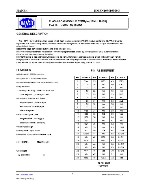
SIMMTOP VIEWNote: A11 is not used for HMD8M32M16EGGENERAL DESCRIPTIONThe HMD8M32M16EG is a 8M x 32bit dynamic RAM high density memory module. The module consists of sixteen CMOS 4M x 4bit DRAMs in 24-pin SOJ packages mounted on a 72-pin, double-sided, FR-4-printed circuit board. A 0.1 or 0.22uF decoupling capacitor is mounted on the printed circuit board for each DRAM components. The module is a single In-line Memory Module with edge connections and is intended for mounting in to 72-pin edge connector sockets. All module components may be powered from a single 5V DC power supply and all inputs and outputs are TTL-compatible.FEATURESw Part IdentificationHMD8M32M16EG- 2048 Cycles/32ms Ref. Gold w Access times : 50, 60ns w High-density 32MByte design w Single + 5V ±0.5V power supply w JEDEC standard PDpin and pinout w EDO mode operationw TTL compatible inputs and outputs w FR4-PCB designOPTIONS MARKINGw Timing50ns access -5 60ns access -6 w Packages72-pin SIMM MPRESENCE DETECT PINSPin 50ns 60ns PD1 NC NC PD2 Vss Vss PD3 Vss NC PD4VssNCPERFORMANCE RANGESpeed tRAC tCAC tRC tHPC 5 50ns 13ns 90ns 26ns 6 60ns15ns110ns30nsPIN SYMBOL PIN SYMBOL PIN SYMBOL 1 Vss 25 DQ22 49 DQ8 2 DQ0 26 DQ7 50 DQ24 3 DQ16 27 DQ23 51 DQ9 4 DQ1 28 A7 52 DQ25 5 DQ17 29 NC 53 DQ10 6 DQ2 30 Vcc 54 DQ26 7 DQ18 31 A8 55 DQ11 8 DQ3 32 A9 56 DQ27 9 DQ19 33 NC 57 DQ12 10 Vcc 34 NC 58 DQ28 11 NC 35 NC 59 Vcc 12 A0 36 NC 60 DQ29 13 A1 37 NC 61 DQ13 14 A2 38 NC 62 DQ30 15 A3 39 Vss 63 DQ14 16 A4 40 /CAS0 64 DQ31 17 A5 41 /CAS2 65 DQ15 18 A6 42 /CAS3 66 NC 19 A10 43 /CAS1 67 PD1 20 DQ4 44 /RAS0 68 PD2 21 DQ20 45 /RAS1 69 PD3 22 DQ5 46 NC 70 PD4 23 DQ21 47 /WE 71 NC 24DQ648NC72VssPIN ASSIGNMENTFUNCTIONAL BLOCK DIAGRAM/RAS1ABSOLUTE MAXIMUM RATINGSPARAMETER SYMBOL RATINGVoltage on Any Pin Relative to Vss V IN ,OUT-1V to 7.0VVoltage on Vcc Supply Relative to Vss Vcc -1V to 7.0VPower Dissipation P D16WStorage Temperature T STG-55o C to 150o CShort Circuit Output Current I OS50mAw Permanent device damage may occur if " Absolute Maximum Ratings" are exceeded. Functional operation should be restricted to the conditions as detailed in the operational sections of this data sheet. Exposure to absolute maximum rating conditions for extended periods may affect device reliability.RECOMMENDED DC OPERATING CONDITIONS( Voltage reference to V SS, T A=0 to 70 o C )PARAMETER SYMBOL MIN TYP. MAX UNIT Supply Voltage Vcc 4.5 5.0 5.5 V Ground Vss 0 0 0 V Input High Voltage V IH 2.4 - Vcc+1 V Input Low Voltage V IL-1.0 - 0.8 VDC AND OPERATING CHARACTERISTICSSYMBOL SPEED MIN MAX UNITS-5 - 816 MaI CC1-6 - 736 MAI CC2Don't care - 32 MA-5 - 816 MAI CC3-6 - 736 MA-5 - 896 MAI CC4-6 - 816 MAI CC5Don't care - 16 MA-5 - 816 MAI CC6-6 - 736 MAI l(L)-80 80 µAI O(L)-10 10 µAV OH 2.4 - VV OL- 0.4 VI CC1 : Operating Current * (/RAS , /CAS , Address cycling @t RC=min.)I CC2 : Standby Current ( /RAS=/CAS=V IH )I CC3 : /RAS Only Refresh Current * ( /CAS=V IH, /RAS, Address cycling @t RC=min )I CC4 : Fast Page Mode Current * (/RAS=V IL, /CAS, Address cycling @t PC=min )I CC5 : Standby Current (/RAS=/CAS=Vcc-0.2V )I CC6 : /CAS-Before-/RAS Refresh Current * (/RAS and /CAS cycling @t RC =min ) I IL : Input Leakage Current (Any input 0V ≤ V IN ≤ 6.5V, all other pins not under test = 0V) I OL : Output Leakage Current (Data out is disabled, 0V ≤ V OUT ≤ 5.5V V OH : Output High Voltage Level (I OH = -5mA ) V OL : Output Low Voltage Level (I OL = 4.2mA )* NOTE : I CC1, I CC3, I CC4 and I CC6 are dependent on output loading and cycle rates. Specified values are obtained with the output open. I CC is specified as an average current. In I CC1 and I CC3, address cad be changed maximum once while /RAS=V IL . In I CC4, address can be changed maximum once within one page mode cycle.CAPACITANCE ( T A =25oC, Vcc = 5V, f = 1Mz )DESCRIPTIONSYMBOL MIN MAX UNITS Input Capacitance (A0-A11) C IN1 - 100 pF Input Capacitance (/W) C IN2 - 130 pF Input Capacitance (/RAS0) C IN3 - 40 pF Input Capacitance (/CAS0-/CAS3) C IN4 - 30 pF Input/Output Capacitance (DQ0-31) C DQ1-20pFAC CHARACTERISTICS ( 0 o C ≤ T A ≤ 70o C , Vcc = 5V ±10%, See notes 1,2.)-5-6 STANDARD OPERATION SYMBOL MINMAXMIN MAXUNITRandom read or write cycle time t RC 90 110ns Access time from /RAS t RAC 50 60 ns Access time from /CASt CAC 13 15 ns Access time from column address t AA 25 30 ns /CAS to output in Low-Z t CLZ 3 3 ns Output buffer turn-off delay t OFF 3 13 3 13 ns Transition time (rise and fall) t T 2 50 2 50 ns /RAS precharge time t RP 30 40 ns /RAS pulse width t RAS 50 10K 60 10K ns /RAS hold time t RSH 13 15 ns /CAS hold time t CSH 38 45 ns /CAS pulse width t CAS 8 10K 10 10K ns /RAS to /CAS delay timet RCD 20 37 20 45 ns /RAS to column address delay time t RAD 15 25 15 30 ns /CAS to /RAS precharge time t CRP 5 5 ns Row address set-up time t ASR 0 0 ns Row address hold time t RAH 10 10 ns Column address set-up timet ASCnsColumn address hold time t CAH8 10 ns Column Address to /RAS lead time t RAL25 30 ns Read command set-up time t RCS0 0 ns Read command hold referenced to /CAS t RCH0 0 ns Read command hold referenced to /RAS t RRH0 0 ns Write command hold time t WCH10 10 ns Write command hold referenced to /RAS t WCR50 55 ns Write command pulse width t WP10 10 ns Write command to /RAS lead time t RWL13 10 ns Write command to /CAS lead time t CWL8 10 ns Data-in set-up time t DS0 0 ns Data-in hold time t DH8 10 ns Refresh period t REF32 32 ns Write command set-up time t WCS0 0 ns/CAS setup time (C-B-R refresh) t CSR 5 5 ns/CAS hold time (C-B-R refresh) t CHR10 10 ns/RAS precharge to /CAS hold time t RPC 5 5 ns Access time from /CAS precharge t CPA30 35 ns/CAS precharge time (Fast page) t CP8 10 ns/RAS pulse width (Fast page ) t RASP50 200K 60 200K nst WRP10 10 ns/W to /RAS precharge time (C-B-Rrefresh)/W to /RAS hold time (C-B-R refresh) t WRH10 10 ns NOTES1.An initial pause of 200µs is required after power-up followed by any 8 /RAS-only or /CAS-before-/RAS refresh cycles before proper device operation is achieved.2.V IH (min) and V IL (max) are reference levels for measuring timing of input signals. Transition times are measured between V IH(min) and V IL(max) and are assumed to be 5ns for all inputs.3.Measured with a load equivalent to 1TTL loads and 100pF4.Operation within the t RCD(max) limit insures that t RAC(max) can be met. t RCD(max) is specified as a reference point only. If t RCD is greater than the specified t RCD(max) limit, then access time is controlled exclusively by t CAC.5.Assumes that t RCD≥ t RCD(max)6. t AR, t WCR, t DHR are referenced to t RAD(max)7.This parameter defines the time at which the output achieves the open circuit condition and is not referenced to V OHor V OL.8. t WCS, t RWD, t CWD and t AWD are non restrictive operating parameter.They are included in the data sheet as electrical characteristic only. If t WCS≥tWCS(min) the cycle is an early writecycle and the data out pin will remain high impedance for the duration of the cycle.9. Either t RCH or t RRH must be satisfied for a read cycle.10. These parameters are referenced to the /CAS leading edge in early write cycles and to the /W leading edge in read-write cycles.11. Operation within the t RAD(max) limit insures that t RAC(max) can be met. t RAD(max) is specified as a reference point only. If t RAD is greater than the specified t RAD(max) limit. then access time is controlled by t AA .TIMING DIAGRAMSTIMING WAVEFORM OF READ CYCLENOTE/RAS/CASA/W/OE DQ0-DQ7 V V OL /RAS /CAS A /W /OE DQ0-DQ7 V IH- V IL-V IH- V IL- V IH- V IL - V IH- V IL- V IH- V IL-V V V IH- V IL-V IH- V IL- V V V V V IH- V0.25 mm MAXPACKAGING INFORMATIONSIMM DesignORDERING INFORMATIONPart NumberDensityOrg.PackageComponent Number VccAccess TimeHMD8M32M16EG-5 32MByte 8MX 32bit 72Pin-SIMM 16EA 5V 50ns HMD8M32M16EG-6 32MByte8MX 32bit72Pin-SIMM16EA5V60ns。