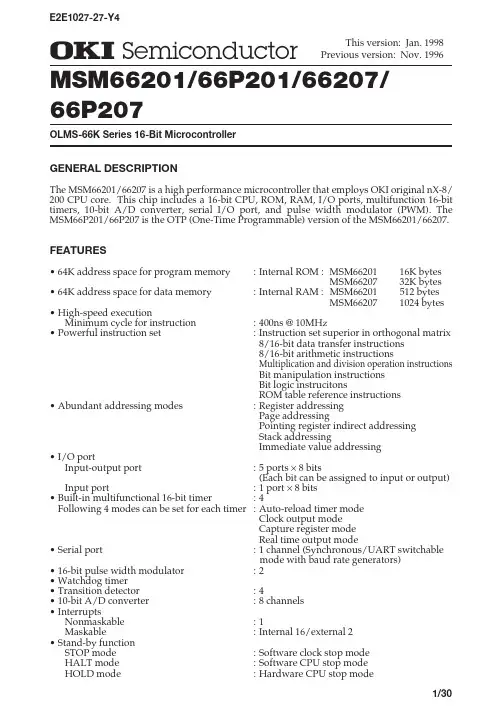
66P207OLMS-66K Series 16-Bit MicrocontrollerGENERAL DESCRIPTIONThe MSM66201/66207 is a high performance microcontroller that employs OKI original nX-8/ 200 CPU core. This chip includes a 16-bit CPU, ROM, RAM, I/O ports, multifunction 16-bit timers, 10-bit A/D converter, serial I/O port, and pulse width modulator (PWM). The MSM66P201/66P207 is the OTP (One-Time Programmable) version of the MSM66201/66207.FEATURES•64K address space for program memory:Internal ROM :MSM6620116K bytesMSM6620732K bytes •64K address space for data memory:Internal RAM :MSM66201512 bytesMSM662071024 bytes •High-speed executionMinimum cycle for instruction:400ns @ 10MHz•Powerful instruction set:Instruction set superior in orthogonal matrix8/16-bit data transfer instructions8/16-bit arithmetic instructionsMultiplication and division operation instructionsBit manipulation instructionsBit logic instrucitonsROM table reference instructions •Abundant addressing modes:Register addressingPage addressingPointing register indirect addressingStack addressingImmediate value addressing•I/O portInput-output port:5 ports ¥ 8 bits(Each bit can be assigned to input or output) Input port:1 port ¥ 8 bits•Built-in multifunctional 16-bit timer:4Following 4 modes can be set for each timer:Auto-reload timer modeClock output modeCapture register modeReal time output mode•Serial port:1 channel (Synchronous/UART switchablemode with baud rate generators)•16-bit pulse width modulator:2•Watchdog timer•Transition detector:4•10-bit A/D converter:8 channels•InterruptsNonmaskable:1Maskable:Internal 16/external 2•Stand-by functionSTOP mode:Software clock stop modeHALT mode:Software CPU stop modeHOLD mode:Hardware CPU stop mode•Package64-pin plastic shrink DIP (SDIP64-P-750-1.78):(MSM66201-¥¥¥SS) (MSM66P201-¥¥¥SS)(MSM66207-¥¥¥SS) (MSM66P207-¥¥¥SS) 64-pin plastic QFP (QFP64-P-1414-0.80-BK):(MSM66201-¥¥¥GSBK)(MSM66207¥¥¥GS-BK)68-pin plastic QFJ (PLCC) (QFJ68-P-S950-1.27):(MSM66201-¥¥¥JS) (MSM66P201-¥¥¥JS)(MSM66207-¥¥¥JS) (MSM66P207-¥¥¥JS) 64-pin ceramic piggyback (ADIP64-C-750-1.78):(MSM66G207VS)(¥¥¥ indicates the code number.)*The piggyback type is used only for engineering samples.BLOCK DIAGRAMPP P P P P P P P P P P P P P P P AE A D YL ES E NDRD 0/P 0.0D 7/P 0.78 /P 1.015/P 1.7P0P1P2P3P4P5DD¥ 8 ¥ 8PIN CONFIGURATION (TOP VIEW)2012345678910111213141516171819CLKOUT/P2.3AD0/P0.0AD1/P0.1AD2/P0.2AD3/P0.3AD4/P0.4AD5/P0.5AD6/P0.6AD7/P0.7A8/P1.0A9/P1.1A10/P1.2A11/P1.3A12/P1.4A13/P1.5A14/P1.6A15/P1.7P2.0P2.1P2.2P3.7/TM3IO V DD V REF AGND P5.7/AI7P5.6/AI6P5.5/AI5P5.4/AI4P5.3/AI3P5.2/AI2P5.1/AI1P5.0/AI0P4.7/TRNS3P4.6/TRNS2P4.5/TRNS1P4.4/TRNS0P4.3/PWM1P4.2/PWM0P4.1/TM1CK P4.0/TM0CK 4564636261605958575655545352515049484746212223242526272829303132444342414039383736353433RESOUTP3.6/TM2IO ALE P3.5/TM1IO PSEN P3.4/TM0IO RD P3.3/INT1WR P3.2/INT0READYP3.1/RXD EA P3.0/TXD FLT P2.7/RXC RES P2.6/TXC OSC0P2.5/HLDA OSC1P2.4/HOLD GNDNMI64-Pin Plastic Shrink DIPPIN CONFIGURATION (TOP VIEW) (Continued)A8/P1.0A9/P1.1A10/P1.2A11/P1.3A12/P1.4A13/P1.5A14/P1.6A15/P1.7P2.0P2.1P2.2P5.2/AI2P5.1/AI1P5.0/AI0P4.7/TRNS3P4.6/TRNS2P4.5/TRNS1P4.4/TRNS0P4.3/PWM1P4.2/PWM0P4.1/TM1CK P4.0/TM0CK 0.7/A D 70.6/A D 60.5/A D 50.4/A D 40.3/A D 30.2/A D 20.1/A D 10.0/A D 0D DR E FG N DW R R E A D Y E A F L T R E S O S C 0O S C 1G N D N M I H O L D /P 2.4H L D A /P 2.5CLKOUT/P2.3RESOUT ALE PSEN RD T X C /P 2.6R X C /P 2.7T X D /P 3.0R X D /P 3.1I N T 0/P 3.2P3.7/TM3IO P3.6/TM2IO P3.5/TM1IO P3.4/TM0IO P3.3/INT15.7/A I 75.6/A I 65.5/A I 55.4/A I 45.3/A I 364-Pin Plastic QFPPIN CONFIGURATION (TOP VIEW) (Continued)AI3/P5.3AI4/P5.4AI5/P5.5AI6/P5.6AI7/P5.7AGND V REF V DD AD0/P0.0AD1/P0.1AD2/P0.2AD3/P0.3AD4/P0.4AD5/P0.5AD6/P0.6AD7/P0.7P3.2/INT0P3.1/RXD P3.0/TXD P2.7/RXC P2.6/TXC P2.5/HLDA P2.4/HOLD NMI GND OSC1OSC0RES FLT EA READY WRA 8/P 1.0A 9/P 1.1A 10/P 1.2A 11/P 1.3A 12/P 1.4A 13/P 1.5A 14/P 1.6A 15/P 1.7P 2.0P 2.1P 2.2C L K O U T /P 2.3R E S O U T A L E P S E N R D P 5.2/A I 2P 5.1/A I 1P 5.0/A I 0P 4.7/T R N S 3P 4.6/T R N S 2P 4.5/T R N S 1P 4.4/T R N S 0P 4.3/P W M 1P 4.1/T M 1C KP 4.0/T M 0C KN CP 3.7/T M 3I OP 3.6/T M 2I OP 3.5/T M 1I OP 3.4/T M 0I OP 3.3/I N T 1V DD N C P 4.2/P W M 0GNDNC : No-connection pin 68-Pin Plastic QFJ (PLCC)PIN DESCRIPTIONType DescriptionSymbol P0.0–P0.7/AD0–AD7P1.0–P1.7/A8–A15P2.0–P2.2P2.5/HLDA P2.6/T X C AD: Outputs the lower 8 bits of program counter during external program memory fetch, and receives the addressed instruction under the control of PSEN . This pin also outputs the address and outputs or inputs data during an external data memory access instruction, under the control of ALE, RD , and WR . P1:8-bit input-output port. Each bit can be assigned to input or output.A:Outputs the upper 8 bits of program counter (PC 8–15) during external program memory fetch. This pin also outputs the upper 8 bits of address during external data memory access instructions.P2:8-bit input-output port. Each bit can be assigned to input or output.T X C:Transmitter clock input/output pin.P3:8-bit input-output port. Each bit can be assigned to input or output.P2.4/HOLD HOLD:Input pin to request the CPU to enter the hardware power-down state.P3.0/T X D P3.1/R X D P0: 8-bit input-output port. Each bit can be assigned to input or output.I/OI/OI/OT X D:Transmitter data output pin.I/OHLDA:HOLD ACKNOWLEDGE: the HLDA signal appears in response to the HOLD signal and indicates that the CPU has entered the power-down state.P2.3/CLKOUT CLKOUT:Output pin for supplying a clock to peripheral circuits.P2.7/R X C R X C:Receiver clock input/output pin.P3.2/INT0R X D:Receiver data input pin.P3.3/INT1INT :Interrupt request input pin.Falling edge trigger or level trigger is selectable.P3.4/TM0IO TM0IO-TM3IO:One of the following signals is output or input.P3.5/TM1IO P3.6/TM2IO P3.7/TM3IO•Clock at twice the frequency range of the 16-bit timer overflow •Load trigger signal to the capture register input •Setting value outputWhether the signal is input or output depends on the mode.P4.0/TM0CK P4:8-bit input-output port. Each bit can be assigned to input or output.P4.1/TM1CK TM0CK, TM1CK:Clock input pins of timer 0, timer 1.P4.2/PWM0P4.3/PWM1P4.4 – P4.7/TRANS0 – TRANS3TRANS:Transition detector.The input pins which sense the falling edge and set the flag.PWM:16-bit pulse-width modulator output pin.I/OP5.0 – P5.7/AI0 –AI7P5:8-bit input port.AI:Analog signal input pin for A/D converter.IPIN DESCRIPTION (Continued)RESOUT Outputs "H" level in the case of internal reset.Reset to"L" level by program.ALEAddress Latch Enable:PSEN Program Strobe Enable:RD Output strobe activated during a bus read cycle.Used to enable data onto the bus from the external data memory.WR Output strobe during a bus write cycle.Used as write strobe to external data memory.I READY Used when the CPU accesses low-speed peripherals.EA Normaly set to "H" level.If set to "L" level, the CPU fetches the code from external program memory.FLT If FLT is "H" level, ALE, WR , RD , PSEN are set to "H" level when reset.If FLT is set to "L", ALE, WR , RD , PSEN are set to floating level when reset.RES RESET input pin.OSC0OSC1Basic clock oscillation pin.NMI Non-maskable interrupt input pin (falling edge).V REF Reference voltage input pin for A/D converter.AGND Ground for A/D converter.V DD System power supply.GNDGround.Type DescriptionSymbol O OO O O I I I I I O ————The timing pulse to latch the lower 8 bits of the address output from port 0 when the CPU accesses the external memory.The strobe pulse to fetch to external program memory.Basic clock oscillation pin.REGISTERSAccumulatorACC15Control Register (CR)PSWBit 15 : Carry flag (CY)Bit 14 : Zero flag (ZF)Bit 13 : Half carry flag (HC)Bit 12 : Data descriptor (DD)Bit 8 : Master interrupt priority flag (MIP)Bit 9,5,4: User flag (MIP)Bit 2-0 : System control base 2-0 (SCB2-0)PC LRB SSP15150Index Register 1Index Register 2Data Pointer User Stack PointerPointing Register (PR)Local RegisterR1R3R5R7R0R2R4R6ER0ER1ER2ER3707SFRAddress (HEX)Name Symbol R/W8/16-bitOperationReset0000 0001 0002 0003 0004I 0005I 0006 0007 0010I 0011 0012I 0013 0018 0019 001A 001B 001C I System stack printerLocal register baseProgram status wordAccumulatorStandby control registerWatchdog timerPeripheral control registerStop code acceptorInterrupt request registerInterrupt enable registerExternal Iinterrupt control registerSSP(ASSP)LRB(ALRB)PSWL(APSW)PSWHACCSBYCONWDTPRPHFSTPACPIEEXICONIRQR/WWR/WW8/1688/16FFHFFHundefinedC8H0CH00H00HF8HFDH"0"00H00H00H00HFCH00H/WDTis stopped0020 0021 0022 0023 0024 0025 0026I 0028 0029 002A 002C 002D 002E 002F 0030 0031Port 0 data registerTimer 0 counterP3IOP3SFP4P4IOTM0R/W8undefined Port 0 mode registerPort 2 secondary function control registerP3P2SFP2IOP2P1IOP1P0IOP0P4SFPort 5P500320033Timer 0 register TMR0 00340035Timer 1 counter TM10036 0037Timer 1 register TMR1Port 1 data registerPort 1 mode registerPort 2 data registerPort 2 mode registerPort 3 secondary function control registerPort 3 data registerPort 3 mode registerPort 4 secondary function control registerPort 4 data registerPort 4 mode registerRR/W1600Hundefined00Hundefined00H07Hundefined00H00Hundefined00H00H—00H00H00H00H00H00H00H00HNote: A I mark in the address column indicates that there is a bit that does not exist in the register.Addres (HEX)Name AbbreviatedNameR/W8/16-bitOperationReset003A 003B 003C 003D 003E 003F 0040 0041 0042 0043 0046I 0048 0049 004A I004C 004D Timer 2 registerTCON2TCON3TRNSITSTTM1600HTimer 0 control registerTCON1TCON0TMR3TM3TMR2STTMRSTTMC004E I0050I 0051 0054 0055 0056I 0058I 0059I Timer 3 counterTimer 3 registerTimer 3 control registerTimer 1 control registerTimer 2 control registerTransition detector registerSerial port transmission baud rate generator counter00H00H00H00H00H00H00H00H00Hundefined00H00H0CH00H00H0EH80Hundefined00HundefinedF0H80HA0HSRTMSRTMRSRTMCSTCONSerial port transmission baud rate generator registerSerial port transmission baud rate generator controlregisterSerial port transmission mode control registerSerial port transmission data buffer registerSerial port receiving error registerA/D scan mode registerA/D select mode registerA/D conversion result register 0Serial port receiving baud rate generator counterSerial port receiving baud rate generator registerSerial port receiving baud rate generator controlregisterSerial port receiving mode control registerSerial port receiving data buffer register0060I 0061STBUFSRCONSRBUFSRSTATADSCANADSELADCR0R/WWR/WRR/WR88/16undefined0038 0039Timer 2 counter00HTM200HSFR (Continued)Note: A I mark in the address column indicates that there is a bit that does not exist in the register.SFR (Continued)Note: A I mark in the address column indicates that there is a bit that does not exist in theregister.Address (HEX)NameAbbreviated NameR/W8/16-bit operationReset0062I 0063A/D conversion result register 1ADCR10064I 0065ADCR20066I 0067ADCR30068I 0069ADCR4006A I 006B ADCR5R8/16undefined006C I 006D ADCR6006E I 006F ADCR700700071PWMC000H 00H 00720073PWM 0 register PWMR000H 00H 00740075PWM 1 counter PWMC100H 00H 00760077PWM 1 register PWMR100H 00H 0078007APWM 0 control register PWCON000H 00H8PWM 1 countrol registerPWCON1R/WA/D conversion result register 2A/D conversion result register 4A/D conversion result register 5A/D conversion result register 6A/D conversion result register 7PWM 0 counter A/D conversion result register 3ADDRESSING MODESThe MSM66201/66207 provides independent 64K-byte data and 64K-byte program space with various types of addressing modes. These modes are shown below, for both RAM (for data space) and ROM (for program space).1.RAM Addressing Modes (for data space)1.1Register Direct Addressing1.2Displacement Addressinga)Zero Pageb)Direct Page1.3Pointing Register (PR) Indirect AddressingData Point (DP) Indirecta)b)User Stack Pointer (USP) Indirectc)Index Register (X1, X2) Indirect1.4Immediate Addressing2.ROM Addressing Modes (for program space) 2.1Direct Addressing2.2Simple Indirect Addressinga)Local Register Indirectb)Pointing Register Indirect1)Data Pointer (DP) Indirect2)User Stack Pointer (USP) Indirect3)Index Register (X1, X2) Indirectc)System Stack Pointer (SSP) Indirectd)Local Register Base (LRB) Indirecte)RAM Indirect2.3Double Indirect Addressinga)Data Pointer (DP) Double Indirectb)User Stack Pointer (USP) Double Indirectc)Index Register (X1, X2) Double Indirect2.4Indirect Addressing with 16-bit Offseta)Pointing Register Indirect 1)Data Pointer (DP) Indirect2)User Stack Pointer (USP) Indirect3)Index Register (X1, X2) Indirectb)RAM IndirectMEMORY MAPS Program Memory Space0000H 7FFFH * FFFFH0000H0027H0028H0037H0038H7FFFH *InternalROM AreaVectorTableArea(40 bytes)ExternalMemoryVCALTableArea(16 bytes) * MSM66201 : 3FFFHData Memory SpaceFFFFH0000H007FH0080H00BFH00C0H047FH *SFR Area SpecialFunctionRegistorsPORT, A/DC,TIMER, PWM,etc....PR AreaPR0PR1PR2PR3PR4PR5PR6PR7(Low Order)X2DPUSP* MSM66201 : 027FH(High Order)80828486X1ABSOLUTE MAXIMUM RATINGSParameter Supply Voltage Input Voltage Output VoltageAnalog Input VoltagePower DissipationStorage Temperature SymbolV DDConditionGND=AGND=0V—Rating–0.3 to 7.0UnitV IV OV AIP DT STG64-pin shrink DIP64-pin QFP–0.3 to V DD+0.3–0.3 to V DD+0.3–0.3 to V REF930565–55 to +150VmW°CAnalog Ref. Voltage V REF–0.3 to V DD+0.3Ta=85°Cper Package68-pin QFJ1120(Ta=25°C) RECOMMENDED OPERATING CONDITIONSParameter Supply Voltage Memory Hold Voltage Operating Frequency Ambient TemperatureFan Out SymbolV DDCondition Range4.5 to5.5UnitV DDHf OSCNMOS loadP02.0 to 5.50 to 10202VMHz—Ta–40 to +85°C TTL loadP1, P2, P3, P41f OSC £ 10MHzf OSC = 0HzV DD = 5V ±10%—ELECTRICAL CHARACTERISTICSDC CharacteristicsNote:1Applied to P02Applied to P1, P2, P3 and P43Applied to P54Applied to ALE, PSEN , RD , WR and RESOUT 5Applied to RES and NMI 6Applied to READY and EA 7Applied to FLT 8Applied to OSC 0*V DD or GND for ports serving as the input pin. No load for any other.**Applied to MSM66P201/66P207ParameterSymbolConditionMin.Max.Unit"H" Input Voltage 1, 3, 6"H" Input Voltage 5, 7V IH2.44.04.23.6V DD +0.3V DD +0.3V DD +0.3V DD +0.3—"H" Input Voltage 8"H" Input Voltage 2Typ.—"L" Input Voltage 1, 2, 3, 6V IL–0.3–0.3–0.30.80.80.4V"L" Input Voltage 5, 7"L" Input Voltage 8V OH 4.24.2——I O = –400m A "H" Output Voltage 1, 4"H" Output Voltage 2V OL——0.40.4I O = 3.2mA "L" Output Voltage 1, 4"L" Output Voltage 2I O = –200m A I O = 1.6mAInput Leakage Current 3, 6, 7I IH /I IL———1/–11/–2010/–10m AV I = V DD /0VInput Current 5Input Current 8"H" Output Current 1"H" Output Current 2I OHI OL –2–1105————mAV O = 2.4V"L" Output Current 1"L" Output Current 2I LO —±2m A Output Leakage Current 1, 2, 4V O = V DD /0V C I C O ————pF Input Capacitance Output Capacitance 57f = 1MHz Ta = 25°C I DDS ——10100m ACurrent Consumption (during STOP) *0.21V DD = 2V I DDH —**—1015Current Consumption (during HALT)68f OSC = 10MHz No LoadI DD—**—3540mACurrent Consumption2030———————————————————(V DD = 5V ± 10%, Ta = –40 to +85°C) I REF ——210Analog Reference Power Supply Current 0.30.5A/D in operation A/D stopped mA m A —AC Characteristics•External program memory control•External data memory controlParameter Symbol ConditionMin.Max.Unit Clock (OSC) Pulse ALE Pulse Width RD Pulse Width WR Pulse Width RD Pulse Delay Time WR Pulse Delay Time Low Address Setup Time Low Address Hold Time High Address Setup Time Data Hold Timet f W t AW t RW t WW t RAD t WAD t AAS t AAH t AAD t DH—C L = 50pF 503t f W –204t f W –204t f W –20t f W –20t f W –202t f W –35t f W –20t f W –20t f W –20————t f W +20t f W +202t f W +20t f W +40t f W +40t f W +40ns(V DD =5V±10%, Ta=–40 to +85°C)Data Delay Time t DD t f W –20t f W +40Memory Data Hold Time t MH 0t f W –20Memory Data Setup Time t MS 100—High Address Hold Time t AWH t f W –20t f W +40High Address Hold Time t ARH t f W –20t f W +40Parameter Symbol ConditionMin.Max.Unit Clock (OSC) Pulse ALE Pulse Width PSEN Pulse Width PSEN Pulse Delay Time Low Address Setup time Low Address Hold Time High Address Delay Time High Address Hold Time Instruction Setup Time Instruction Hold Timet f W t AW t PW t PAD t AAS t AAH t AAD t APH t IS t IH—C L = 50pF 503t f W –204t f W –20t f W –202t f W –35t f W –20t f W –20t f W –201000———t f W +202t f W +20t f W +40t f W +40t f W +40—t f W –20ns(V DD =5V±10%, Ta=–40 to +85°C)CLKALEAD0-7A8-15PSENAD0-7A8-15RDAD0-7A8-15WR• Serial port control Master modeSlave modeParameter Symbol ConditionMin.Max.UnitClock (OSC) Pulse Width Serial Clock Pulse Width Input Data Setup Time Input Data Hold Timet f W t SCKW t STMXS t STMXH t SRMXS t SRMXH—508t f W 8t f W +406t f W –202t f W +1050——————ns —C L =50pF Output Data Setup Time Output Data Hold Time (V DD =5V±10%, Ta=–40 to +85°C)Parameter Symbol ConditionMin.Max.UnitClock (OSC) Pulse Width Serial Clock Pulse Width Input Data Setup Time Input Data Hold Timet f W t SCKW t STSXS t STSXH t SRSXS t SRSXH—508t f W 6t f W +406t f W –20100100——————ns —C L =50pF Output Data Setup Time Output Data Hold Time (V DD =5V±10%, Ta=–40 to +85°C)SCKSDOUT (TXD)SDIN (RXD)SCKSDOUT (TXD)SDIN(RXD)A/D Converter Characteristics • Operating range• A/D Converter accuracy Normal operation modeParameter SymbolConditionMin.Unit Resolution Crosstalkn E A E R E CSee the recommendedcircuit.V R =V DD V AG =GND=0V Analog input source impedance£5k WOne channel conversion timet C =64m s————BitAbsolute Error Relative Error *———————±0.5*———±0.510+3.0–3.5±1.5*10±1.0Typ.Max.E Z 0Zero Point Error 0——+3.0+2.0E F –0.5LSBFull Scale Error–1.0——–3.5–3.5Differential Linearity Error E D ——————+3.0+2.0+2.0–3.5(V DD =5V±10%, f OSC =10MHz, Ta=–40 to +85°C)*V DD =5V, Ta=25°CHALT/HOLD operation modeParameter SymbolConditionMin.Unit Resolution Crosstalkn E A E R E CSee the recommendedcircuit.V R =V DD V AG =GND=0VAnalog input source impedance£5k WOne channel conversion timet C =64m s————BitAbsolute Error Relative Error *———————±0.5*———±0.510+2.0–3.5±1.0*10±0.5Typ.Max.E Z +0.5Zero Point Error +0.5——+2.0+1.0E F –1.0LSBFull Scale Error–1.5——–3.5–2.0Differential Linearity Error E D ——————+2.0+1.0+1.0–2.0(V DD =5V±10%, f OSC =10MHz, Ta=–40 to +85°C)*V DD =5V, Ta=25°CParameter Symbol Condition Min.Max.Unit Power Supply Voltage Analog Reference Voltage Operating TemperatureV DD V R V AI R R T opf OSC £ 10MHz4.54.5V AG —–405.5V DD V R —+85V k W °CV AG = GND = 0V Analog Input Voltage Analog Reference Power Voltage Resistance Typ.———16—V DD = 5V ± 10%• Recommended circuit+5V0VR I (Analog input source impedance) £ 5k W• A/D Converter conversion characteristics 13FF000E Z MINE Z MAXVREF [V]Analog InputConversion CodeConversion Characteristics Diagram 1Absolute error (E A )The absolute error indicates a difference between actual conversion and ideal conversion,excluding a quantizing error. The absolute error of the A/D converter gets larger as it approaches the zero point or full scale. (Refer to Conversion Characteristics Diagram 1.)Relative error (E R )The relative error indicates a deviation from a line which connects the center point of the zero point conversion width with that of the full scale conversion width, excluding a quantizing error.The relative error of this A/D converter is almost due to a differential linearity error.Zero point error (Ez) and full scale error (E F )The zero point error and full scale error indicate a difference between actual conversion and ideal conversion at the zero point and full scale, respectively. (Refer to Conversion Characteristics Diagram 1.)A/D Converter Conversion Characteristics 2 (temperature characteristics)Conversion CharacteristicsConversion CharacteristicsDiagram 2-1Diagram 2-2Differential linearity error (E D )The differential linearity error indicates a difference between the actual conversion width (actual step width) and ideal value (1LSB).With this A/D converter, a voltage for actual conversion is shifted and the inclination of a voltage is changed, with changes of temperature (see Conversion Characteristics Diagram 2-1). Specifications described in the foregoing tables are established from Eta shown in Conversion Characteristics Diagram 2-1 (E D =Eta–1LSB). Conversion Characteristics Diagram 2-2 shows temperature characteristics of differential linearity of Es in Conversion Characteristics Diagram 2-1.3FF[HEX]000E SEta[V]–40°C+25°C+85°C+4[LSB]0Temparature Ta+3+2+1–40+85During normal operation During HALTE SConversion CodeAnalog InputESDifferential Linearity[°C](Unit : mm)PACKAGE DIMENSIONSNotes for Mounting the Surface Mount Type PackageThe SOP, QFP, TSOP, SOJ, QFJ (PLCC), SHP and BGA are surface mount type packages, which are very susceptible to heat in reflow mounting and humidity absorbed in storage.Therefore, before you perform reflow mounting, contact Oki’s responsible sales person for the product name, package name, pin number, package code and desired mounting conditions (reflow method, temperature and times).SDIP64-P-750-1.78Package material Lead frame material Pin treatmentSolder plate thickness Package weight (g)Epoxy resin Cu alloySolder plating 5 m m or more 8.70 TYP.(Unit : mm)Notes for Mounting the Surface Mount Type PackageThe SOP, QFP, TSOP, SOJ, QFJ (PLCC), SHP and BGA are surface mount type packages, which are very susceptible to heat in reflow mounting and humidity absorbed in storage.Therefore, before you perform reflow mounting, contact Oki’s responsible sales person for the product name, package name, pin number, package code and desired mounting conditions (reflow method, temperature and times).QFP64-P-1414-0.80-BKPackage material Lead frame material Pin treatmentSolder plate thickness Package weight (g)Epoxy resin 42 alloySolder plating 5 m m or more 0.87 TYP.Mirror finish(Unit : mm)Notes for Mounting the Surface Mount Type PackageThe SOP, QFP, TSOP, SOJ, QFJ (PLCC), SHP and BGA are surface mount type packages, which are very susceptible to heat in reflow mounting and humidity absorbed in storage.Therefore, before you perform reflow mounting, contact Oki’s responsible sales person for the product name, package name, pin number, package code and desired mounting conditions (reflow method, temperature and times).QFJ68-P-S950-1.27Package material Lead frame material Pin treatmentSolder plate thickness Package weight (g)Epoxy resin Cu alloySolder plating 5 m m or more 4.50 TYP.Mirror finish(Unit : mm)Notes for Mounting the Surface Mount Type PackageThe SOP, QFP, TSOP, SOJ, QFJ (PLCC), SHP and BGA are surface mount type packages, which are very susceptible to heat in reflow mounting and humidity absorbed in storage.Therefore, before you perform reflow mounting, contact Oki’s responsible sales person for the product name, package name, pin number, package code and desired mounting conditions (reflow method, temperature and times).ADIP64-C-750-1.78。