讯联电子nRF51822实战教程--2.4G无线通讯
- 格式:pdf
- 大小:6.52 MB
- 文档页数:10

Nordic nRF51822介绍一、为什么大家会选择蓝牙nRF51822 ?nRF51822是功能强大、高灵活性的多协议SoC,非常适用于Bluetooth®低功耗和2.4GHz超低功耗无线应用。
nRF51822 基于配备 256kB flash + 16kB RAM的32位ARM® Cortex™ M0 CPU 而构建。
嵌入式2.4GHz收发器支持蓝牙低功耗及2.4GHz操作,其中2.4GHz模式与 Nordic Semiconductor的nRF24L 系列产品无线兼容。
nRF51822 还具备丰富的模拟和数字周边产品,可以在无需 CPU 参与的情况下通过可编程周边产品互联(PPI)系统进行互动。
灵活的31引脚GPIO映射方案可使I/O(例如串行接口、PWM 和正弦解调器)根据PCB需求指示映射到任何设备引脚。
这可实现完全的设计灵活性及引脚位置和功能。
nRF51822支持S110蓝牙低功耗协议堆栈及2.4GHz协议堆栈(包括Gazell),这两种协议堆栈在nRF518软件开发套件中均免费提供。
nRF51822 需要单独供电,如果供电范围在 1.8-3.6V之间,用户可选择使用芯片上的线性整流器,如果供电范围在 2.1-3.6V 之间,可以选择直流1.8V 模式和芯片上的DCDC 变压器。
DC-DC变压器的使用可在工作期间动态控制,并使nRF51822工作期间的射频峰值电流低于10 mA @ 3V供电(TX @ 0 dBm & RX)。
二、蓝牙nRF51822特点1.单芯片,高灵活性,2.4GHz多协议设备;2.32位ARM Cortex M0 CPU内核;3.256KB flash 16KB RAM;4.支持S110蓝牙低功耗协议堆栈;5.S110需要80kB内存空间;6.线程安全和运行时保护;7.事件驱动API;8.与nRF24L系列无线兼容;9.3种数据率(2Mbps/1Mbps/250kbps);10.+4dBm输出功率;11.-92.5dBm敏感度、蓝牙低功耗;12.用于最大化能源效率应用和代码简化的PPI系统;13.具备对每个周边产品进行自动能源管理的灵活能源管理系统;14.用于模拟和数字I/O的可配置I/O映射。

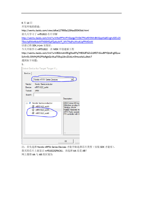
6月14日开发环境的搭建:/view/a9ce127908a1284ac85043dd.html前几天学习了nrf51822芯片详解/link?url=NoIPFYcVFVQiqtgcTIVDbTFKJsfSY0MnBKiQzptXa8Cirghc3ZCx2S TEduYpEMztfAdoMTN08Xf2pFZpAyJbYF_MV7NqPxyWwA1qFPkKOoW以前已将SDK,J-Link安装好。
今天开始学习nRF51822 在MDK中创建新工程/link?url=BGtmdmEEJg3lzoEFq7HB3LBTbZn2L9fD7rGiwBPYQkbR-gEQuw ScXm5L-DIMHjifN2FNsRgbQJv9uaT03cp2AnJZUbLm5htwoIbJLu8tdv7遇到如下问题:1、注:首先选择Nordic nRF51 Series Devices才能开始选择芯片类型(安装SDK才能有)。
我买的芯片上面显示nrf51822QFACA1,该选择AA还是AB?网上搜得AA与AB的区别为只是flash与运行代码大小的区别。
淘宝介绍说该芯片为256Kbflash,所以应该是QFAA。
6月15日关于JLINK用SWD模式与nrf51822的连接。
我连接的是GND(随便哪个地),VCC(pin1),TMS(pin7),TCK(pin9). 网上说可能还得接pin15的复位脚,但是我暂时没接。
接下来就是讲程序烧录看行不行。
1、有个问题,网上找的那个创建工程中并没有用户自己的文件(即像stm32中创建的时候会建立mai.c)不是很明白。
编译能通过,但是load的时候出现问题。
2、Load时出现如下错误:但是reset菜单没找到在哪里?又出现新问题:解决方法:第一次的时候没有遇到这个问题,所以可能是连线没接好,而且后来的jlink总感觉绿灯是闪亮的,很有可能是连线问题。
网上的答案:1.确保接线正确;2. 高版本jlink固件可识别出赝品jlink,而MDK5.x版本要求SEGGER固件高于V4.78,排查是否是盗版jlink导致该问题发生。

【蓝牙BLE系列】NRF51822NRF2810NRF52832NRF2840方案对比NRF51822简介nRF51822是一款功能强大,高度灵活的多协议的SoC,非常适用于蓝牙低功耗和2.4GHz的无线应用。
该SoC是基于ARM Cortex M0为内核的微处理器,拥有256KB/128KB 的片上FLASH存储空间,32KB/16KB的RAM空间。
2.4G无线射频支持蓝牙低功耗,同时兼容nRF24L系列的产品。
其应用领域:手机配件,穿戴式设备,无线充电监控,PC外设,消费电子遥控器,智能家居,智能射频标签,玩具和电子游戏等。
芯片特性✧单芯片,高度灵活的2.4GHz多协议设备✧32位ARM Cortex M0CPU内核✧256KB/128KB闪存+32KB/16KB RAM✧支持蓝牙低功耗协议栈✧线程安全和运行时保护✧事件驱动API支持✧空中链路兼容nRF24L系列✧三种速率:2Mbps/1Mbps/250Kbps✧+4dBm输出功率✧-93dBm灵敏度,蓝牙低功耗✧灵活的电源管理系统✧可配置的I/O✧工作温度范围:-40℃至+105℃NRF52810简介nRF52810是一款支持蓝牙5,ANT和 2.4GHz的高性能多协议的SoC。
该SoC提供了对蓝牙5的支持,同时微处理器内核为ARM Cortex M4,具有192KB的FLASH和24KB的RAM空间,能够提供更多的高级应用的支持。
即使在低功耗的应用之中也是表现得非常出色的。
其应用领域:蓝牙5连接处理器,工业传感器和执行器,穿戴设备,智能家居传感器,电脑外设,体育和健身传感器,智能手表,互动游戏和楼宇自动化等。
芯片特性✧单芯片,高度灵活的2.4GHz多协议SoC✧32位ARM Cortex-M4处理器✧电压范围:1.7V至3.6V✧192kB闪存+24kB RAM✧支持并发蓝牙低功耗/ANT协议操作✧+4dBm的输出功率✧-96dBm灵敏度,蓝牙低功耗✧线程安全和运行时保护✧事件驱动API支持✧空中链路兼容nRF24L和nRF24AP系列✧两种速率:2Mbps/1Mbps✧自动的电源管理系统✧可配置的I/O✧1个主/从SPI✧1x双线接口(I²C)✧UART(RTS/CTS)✧1个PWM(4个通道)✧AES HW加密✧8通道10/12位ADC✧正交解码器64级模拟比较器✧实时时钟(RTC)✧数字麦克风接口(PDM)NRF52832简介nRF52832是一款功能强大,高度灵活的超低功耗多协议的SoC,非常适合蓝牙低功耗(BLE,以前成为智能蓝牙),ANT和 2.4GHz的无线应用。

0、功能简介IC功能包括:256kB片上闪存和16kB RAM;数字和混合信号周边,包括SPI、2-wire、ADC以及正交解码器;16 PPI通道;撘配片上LDO时电源范围为1.8-3.6V,LDO旁路模式为1.75-1.95V ;片上下拉DC/DC转换器用于3V电池(例如,纽扣电池);片上+/- 250 ppm 32kHZ RC振荡器,在蓝牙低功耗应用,不需外部32kHz晶体,可节省成本和电路板空间;6x6mm 48脚QFN封装,提供最多可达32个GPIO;完整的蓝牙协议堆栈(到配置文件的链接层)。
nRF51822的S110是可下载、免版税、预编译二进制蓝牙低功耗堆栈,可独立编程和更新。
功能包括:异步和事件驱动SVC的API;运行时保护;GATT、GAP和L2CAP级别API;周边和广播器角色;GATT客户端和服务器;和2.4GHz RF专用协议的非并行多协议操作;少于128kB的代码和6kB的RAM,为应用程序留有超过128kB的闪存和10kB的RAM;与使用上一代nRF8001的双芯片应用相比,运行S110堆栈的nRF51822削减了高达50%的功耗。
S110堆栈和nRF51822加上nRF518 SDK相互配合,nRF518包含全面的蓝牙低功耗配置文件、服务以及示例应用集合。
1、架构围绕两条内部总线展开:AHB,APB AHB (Advanced High Performance BUS):CPU: ( Cortex-m0,NVIC,BBB,DAP)Memory : ( RAM, Flash)GPIO : P0(P0.0~P0.31)AHB to APB BridgeAPB (Advanced Peripheral BUS):左半边:Power:电源控制WDT:看门狗SPI0,SPI1TIMER0(32位),TIMER1(16位),TIMER2(16位)QDEC:正交译码器,CLOCK:提供两个时钟:HFCLK(16MHZ),LFCLK(32.768KHZ)TWI0,TWI1:两线接口,兼容I2C右半边:NVMC :非易失性存储控制器RADIO: 2.4GHZ 无线广播的数据率:250KBPS,1MBPS,2MBPS ECB: 加密功能(AES),产生HASH序列,数字签名,生成密钥流等RNG:产生随机数用于加密(基于内部热噪声),无需种子值。
nRF51 Development KitDeveloping with the MDK-ARM Microcontroller Development Kit User Guide v1.0Copyright © 2014 Nordic Semiconductor ASA. All rights reserved.Reproduction in whole or in part is prohibited without the prior written permission of the copyright holder.1 IntroductionThe nRF51 Development Kit combined with the nRF51 SDK forms a complete solution for product development based on nRF51 series chips.The nRF51 Development Kit is fitted with the nRF51422 chip, which is a powerful, highly flexible multi-protocol System on Chip (SoC) ideally suited for ANT™/ANT+, Bluetooth® low energy (BLE), and 2.4 GHz proprietary ultra-low power wireless applications.And, if you are not using the ANT protocol, you can use the nRF51822 chip in your end product - without any changes needed to your code.1.1Key featuresThe nRF51 DK board has the following key features:•nRF51422 flash based ANT/ANT+, Bluetooth low energy SoC solution•2.4 GHz compatible with nRF24L devices•Buttons and LEDs for user interaction•I/O interface for Arduino form factor plug-in modules•SEGGER J-Link OB Debugger with debug out functionality•Virtual COM Port interface via UART•Drag and drop Mass Storage Device (MSD) programming•mbed enabled1.2Required toolsBelow is a list of hardware and software tools that is required if you plan to explore all the features on this development kit. All the tools may not be required for all use cases.Nordic Tools DescriptionnRFgo Studio nRFgo Studio is our tool to program and configure devices. It supports the programming ofnRF51 SoftDevices, applications, and bootloaders. The different programming modes areavailable on individual tabs in the nRF51 programming module. Studio is used for thefollowing:•Bluetooth Direct Test Mode (DTM) testing•Erasing flash memory•Programming a SoftDevice•Programming an application•Programming the bootloadernRFgo Studio supports programming of SEGGER J-Link based nRF51 devices.For more information, see the help in nRFgo Studio.nRF51 Tools nRF51 Tools is a package that contains JLinkARM, JLink CDC, nRFjprog, and mergehex.The nRFjprog is a command line tool for programming nRF51 series chips. It is also useful in aproduction setup.nRF51 Tools will be installed together with nRFgo Studio.nRF51 SDK The nRF51 Software Development Kit (SDK) provides source code of examples and librariesforming the base of your application development. The nRF51 SDK includes:•Example code•ANT profile examples•Bluetooth profile examples•Drivers•LibrariesFor more information, see the documentation packaged with the nRF51 SDK.Master Control Panel The Master Control Panel is the software tool that is used with the nRF51 Dongle (PCA10031) to act as a Bluetooth low energy peer device. You can test your application’s wireless connectionwith this tool.The Master Control Panel supports programming of SEGGER J-Link based nRF51 devices.For more information, see the help files in the Master Control Panel.nRF Master Control Panel for Android 4.3nRF Master Control Panel for Android 4.3 is a powerful generic tool that allows you to scan and explore your Bluetooth Smart devices and communicate with them on an Android phone. MCP supports a number of Bluetooth SIG adopted profiles including the Device Firmware Update (DFU) profile from Nordic Semiconductor.S110 SoftDevice Bluetooth low energy Peripheral/Broadcaster protocol stack. For more information, see the S110 nRF51822 SoftDevice Specification and the nRF51 SDK documentation.S120 SoftDevice Bluetooth low energy Central protocol stack solution supporting up to eight simultaneous Central role connections. For more information, see the S120 nRF51822 SoftDevice Specificationand the nRF51 SDK documentation.S130 SoftDevice Bluetooth Smart concurrent multi-link protocol stack solution supporting simultaneous Central/ Peripheral/Broadcaster/Observer role connections. For more information, see the S130nRF51822 SoftDevice Specification and the nRF51 SDK documentation.S210 SoftDevice ANT protocol stack. For more information, see the S210 nRF51422 SoftDevice Specification and the nRF51 SDK documentation.S310 SoftDevice ANT and Bluetooth low energy Peripheral controller and host multiprotocol stack. For more information, see the S310 nRF51422 SoftDevice Specification and the nRF51 SDK documentation.1.3DocumentationBelow is a list of the core documentation for the nRF51 Series and the nRF51x22 chip.Note: See our website for additional documentation such as Application Notes and White Papers.Third party toolsDescriptionKeil MDK-ARM Development Kit Keil MDK-ARM Development Kit is a development environment specifically designed formicrocontroller applications that lets you develop using the nRF51 SDK application and example files.SEGGER J-Link Software The J-Link software is required to debug using the J-Link hardware that is packaged with this development kit.ANTware IIANTWare is an application used for the control of ANT wireless devices. It is an excellent tool for first time ANT developers to explore the capabilities of ANT as a low power wireless solution, and for experienced users to easily setup and monitor advanced ANT networks. ANTWare II improves upon past versions with a slick new interface, streamlined functions, and a variety of new features.DocumentDescriptionnRF51 Series Reference ManualThe nRF51 Series Reference Manual is a functional description of all the modules and peripherals supported by the nRF51 series.nRF51x22 Product SpecificationThe nRF51x22 Product Specification contains all specifications specific to the chip.S110 nRF51822 SoftDevice SpecificationThe S110 nRF51822 SoftDevice Specification contains information about the SoftDevice features and performance.S120 nRF51822 SoftDevice SpecificationThe S120 nRF51822 SoftDevice Specification contains information about the SoftDevice features and performance.S130 nRF51822 SoftDevice SpecificationThe S130 nRF51822 SoftDevice Specification contains information about the SoftDevice features and performance.S210 nRF51422 SoftDevice SpecificationThe S210 nRF51422 SoftDevice Specification contains information about the SoftDevice features and performance.S310 nRF51422 SoftDevice SpecificationThe S310 nRF51422 SoftDevice Specification contains information about the SoftDevice features and performance.nRF51 SDK DocumentationThe nRF51 SDK documentation includes user guides, descriptions, and reference material to help you understand the protocols, examples, and other components of the SDK.nRF51x22 Product Anomaly NotificationThe nRF51x22 Product Anomaly Notification - list of anomalies relevant for the chip.ANT Message Protocol and UsageThe ANT Message Protocol and Usage document describes the ANT protocol in detail and contains the fundamental knowledge you need in order to develop successfully with ANT.nRF51 Development Kit Hardware FilesThe nRF51 Development Kit includes firmware source code, documentation, hardware schematics, and layout files. Included are the following files:•Altium Designer files •Schematics •PCB layout files •Production files•Assembly drawings •Drill files •Gerber files•Pick and Place files •Bill of Materials1.4Development Kit release notesDate Kit version Description October 2014 1.0•First release.2 Kit contentIn addition to hardware, the nRF51 Development Kit consists of firmware source code, documentation, hardware schematics, and layout files which are available from .Figure 1 nRF51 Development Kit content1 x3V CR2032Lithium battery5 x nRF51422 samples1 x nRF51 Development Kit board (PCA10028)3 GettingstartedThis section shows you how to get access to the tools, libraries, and documentation.Connect your nRF51 Development Kit to a computer.1.Connect your nRF51 DK board to a computer with a USB cable.2.The status light (LD5) will come on, indicating it has power.3.After a few seconds, the computer will recognize the nRF51 DK board as a standard USB drive.Figure 2 Windows exampleGet started with the toolchain and examples.1.Download and install nRFgo Studio (which includes the nRF Tools package; JLinkARM, JLink CDC,nRFjprog, and mergehex) from .2.Download and install the latest Keil MDK-ARM from /arm.3.Download and install the latest nRF51 SDK found on .4.Read the information in the Readme.txt file that is installed together with the SDK.After the installation, the SDK documentation is found here:Online: /nRF51_SDK/doc/index.html.Offline: <keil_location>/ARM/Pack/NordicSemiconductor/nRF_Examples/<version>/documentationThe nRF51 DK board is equipped with a boot/reset button (SW5). This button is connected to the interface MCU on the board and have two functions:•Reset button for the nRF device.•Enter boot loader mode of the interface MCU.During normal operation the button will function as a reset button for the nRF device. To enter boot loader mode of the Interface MCU, the button must be pressed while the board is powered until the LED LD5 starts to blink. This is done by pressing the reset button and power cycle the board, either by disconnecting and reconnecting the USB cable or toggle the power switch (SW6).4.2Virtual COM portThe on-board Interface MCU features a Virtual COM port via UART.•Flexible baudrate setting up to 1 Mbps•Dynamic Hardware Flow Control (HWFC) handling•Tri-stated UART lines while no terminal is connectedTable 1 shows an overview of the UART connections on nRF51422 and the interface MCU.nRF51422Interface MCUDefault GPIO UART UARTP0.08RTS CTSP0.09TXD RXDP0.10CTS RTSP0.11RXD TXDTable 1 Relationship of UART connections on nRF51422 and Interface MCUThe UART signals are routed directly to the Interface MCU. The UART pins connected to the Interface MCU is tri-stated when no terminal is connected to the Virtual COM port on the computer.Note: The terminal used must send a DTR signal in order to configure the UART Interface MCU pins. The P0.08 (RTS) and P0.10 (CTS) can be used freely when HWFC is disabled on the nRF51422.4.3Interface MCU FirmwareThe on board Interface MCU is factory programmed with an mbed compliant bootloader, this feature enables the ability to swap interface FW between the factory preloaded SEGGER J-Link OB and the nRF51 mbed interface FW, see section 4.1 “IF Boot/Reset button” on page8 on how to enter the bootloader.To swap Interface MCU FW, simply drag the Interface image (.bin) into the mounted bootloader drive on the connected computer and power cycle the board.Both the nRF51 mbed interface FW and the J-Link OB image can be downloaded from.Note: If you have swapped to the mbed image and want to revert back to the J-Link image, download the latest SEGGER J-Link software from and open a debug sessionto update to the latest J-Link OB firmware version.Note: The J-Link serial number is linked to the Interface MCU and will not change even when swapping the Interface MCU FW, so it can be useful to write the serial number on a sticker onthe board.5 HardwaredescriptionThis chapter describes the nRF51 Development Kit board (PCA10028).Figure 5 nRF51 DK board bottom5.2Block diagramFigure 6nRF51 DK board block diagramFigure 7 Power supply optionsThe 5 V from the USB is regulated down to 3.3 V through an on-board voltage regulator. The battery and external power supply are not regulated. The power sources are routed through a set of diodes (D1A, D1B, and D1C) for reverse voltage protection, where the circuit is supplied from the source with the highest voltage.Note: When not USB powered, the Interface MCU is in dormant state and will draw an additional current of ~ 20 μA in order to maintain the reset button functionality. This will affect boardcurrent consumption, but will not affect the nRF51 current measurements as described inSection 5.7 “Measuring current” on page18.5.4Connector interfaceAccess to the nRF51422 GPIOs is available at connectors P2, P3, P4, P5, and P6 on the nRF51 DK board.In addition there is access to ground and power on the P1 connector.Figure 10 nRF51 DK board connectorsThe signals are also available on bottom side connectors P7, P8, P9, P10, P11, and P12. By mounting pin lists on the connector footprints, the nRF51 DK board can be used as a shield for Arduino motherboards or other boards that follows the Arduino standard.For easy access to GPIO, power, and ground, the signals can also be found on the through-hole connectors P13-P17.Note: Some pins have default settings.•P0.08, P0.09, P0.10, and P0.11 are by default used by the UART connected to theInterface MCU. See Section 4.2 “Virtual COM port” on page9 for more information.•P0.17 - P0.24 are by default connected to the buttons and LED.See Section 5.5 “Buttons and LEDs” on page16 for more information.•P0.26 and P0.27 are by default used for the 32 kHz crystal and are not available on theconnectors. See Section 5.6 “32.768 kHz crystal” on page17 for more information.When the nRF51 DK board is used as a shield together with an Arduino standard motherboard, the Arduino signals is routed like shown in Figure 11.Figure 11 Arduino signals routing on the nRF51 DK board5.5Buttons and LEDsThe four buttons and four LEDs on nRF51 DK board are connected to dedicated I/Os on the nRF51422 chip. The connections are shown in Table 3.Part GPIO ShortButton 1P0.17-Button 2P0.18-Button 3P0.19-Button 4P0.20-LED 1P0.21SB5LED 2P0.22SB6LED 3P0.23SB7LED 4P0.24SB85.632.768 kHz crystalnRF51422 can use an optional 32.768 kHz crystal (X2) for higher accuracy and lower average power consumption. On the DK board, P0.26 and P0.27 are by default used for the 32.768 kHz crystal and are not available as a GPIO on the connectors.Note: When using ANT/ANT+, the 32.768 kHz crystal (X2) is required for correct operation.5.7Measuring currentThe current drawn by the nRF51422 device can be monitored on the nRF51 DK board. To measure the current, you must first prepare the board by cutting the shorting of solder bridge SB9.There are two ways of measuring the current consumption:1.Connect an ampere-meter between the pins of connector P22. This will monitor the currentdirectly.Figure 16 Current measurement with ampere-meter2.Mount a resistor on the footprint for R6. The resistor should not be larger than 10 Ω. Connect anoscilloscope in differential mode or similar with two probes on the pins of the P1 connector andmeasure the voltage drop. The voltage drop will be proportional with the current consumption.Note: The current measurements will become unreliable when a Serial terminal is connected to the Virtual COM port.5.8RF measurementsThe nRF51 DK board is equipped with a small size coaxial connector for conducted measurements of the RF signal (J1). The connector is of SWF type from Murata (part no. MM8130-2600) with an internal switch. By default, when there is no cable attached, the RF signal is routed to the on-board PCB trace antenna. A test probe is available from Murata, part no. MXHS83QE3000, which has a standard SMA connection on the other end for connecting instruments. When connecting the test probe, the internal switch in the SWF connector will disconnect the PCB antenna and connect the RF signal from the nRF51 device to the test probe.Figure 18 Connecting a spectrum analyzerThe connector and test probe will add loss to the RF signal which should be taken into account when doing measurements, see Table 4.Table 4 Typically loss in connector and test probeFrequency (MHz)Loss (dB)2440 1.04880 1.773202.6The P20 also features a debug out connection in order to program shield mounted targets, as for the Debug out P19 header the Interface MCU will detect the supply voltage on the mounted shield and program/ debug the shield target.If the Interface MCU detects target power on both P19 and P20 it will default to program/debug the target connected to P19Page 21nRF51 Development Kit User Guide v1.0Liability disclaimerNordic Semiconductor ASA reserves the right to make changes without further notice to the product to improve reliability, function or design. Nordic Semiconductor ASA does not assume any liability arising out of the application or use of any product or circuits described herein.Life support applicationsNordic Semiconductor’s products are not designed for use in life support appliances, devices, or systems where malfunction of these products can reasonably be expected to result in personal injury. Nordic Semiconductor ASA customers using or selling these products for use in such applications do so at their own risk and agree to fully indemnify Nordic Semiconductor ASA for any damages resulting from such improper use or sale.Contact detailsFor your nearest distributor, please visit .Information regarding product updates, downloads, and technical support can be accessed through your My Page account on our homepage.Revision historyARM statementKeil, μVision, and Cortex are trademarks of ARM Limited. All other brands or product names are the property of their respective holders.DateVersion DescriptionOctober 2014 1.0•First release.Main office:Phone: +47 72 89 89 00Fax: +47 72 89 89 89 Otto Nielsens veg 127052 Trondheim NorwayMailing address:Nordic Semiconductor P .O. Box 23367004 TrondheimNorway。