
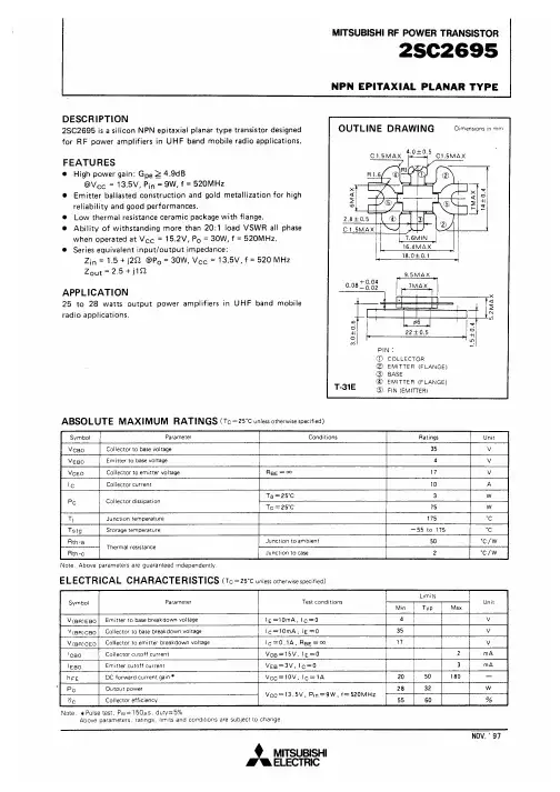
2SC2695中文资料
- 格式:pdf
- 大小:176.72 KB
- 文档页数:4
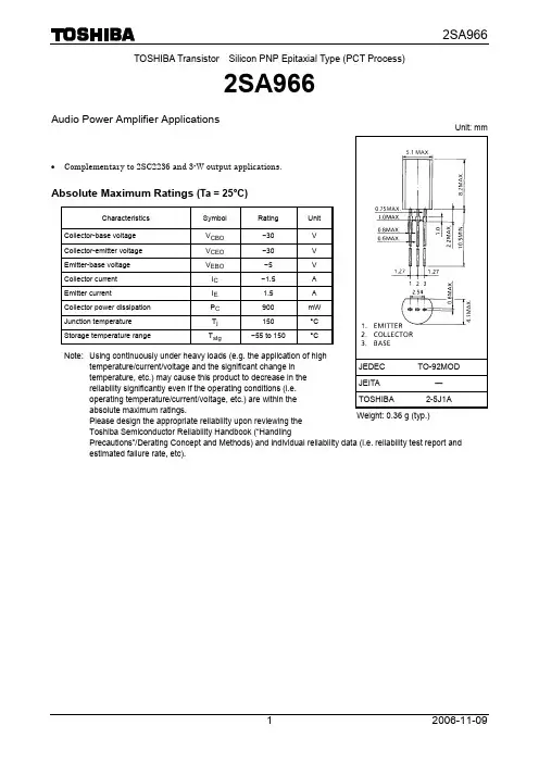
TOSHIBA Transistor Silicon PNP Epitaxial Type (PCT Process)2SA966Audio Power Amplifier Applications• Complementary to 2SC2236 and 3-W output applications.Absolute Maximum Ratings (Ta = 25°C)Characteristics Symbol Rating UnitCollector-base voltage V CBO −30 V Collector-emitter voltage V CEO −30 V Emitter-base voltage V EBO −5 V Collector current I C−1.5 AEmitter currentI E 1.5 A Collector power dissipation P C 900 mW Junction temperature T j 150 °C Storage temperature rangeT stg−55 to 150°CNote: Using continuously under heavy loads (e.g. the application of high temperature/current/voltage and the significant change in temperature, etc.) may cause this product to decrease in thereliability significantly even if the operating conditions (i.e. operating temperature/current/voltage, etc.) are within the absolute maximum ratings.Please design the appropriate reliability upon reviewing the Toshiba Semiconductor Reliability Handbook (“HandlingPrecautions”/Derating Concept and Methods) and individual reliability data (i.e. reliability test report and estimated failure rate, etc).Unit: mmJEDEC TO-92MOD JEITA ―TOSHIBA 2-5J1A Weight: 0.36 g (typ.)Electrical Characteristics (Ta = 25°C)Characteristics Symbol TestCondition MinTyp.Max UnitCollector cut-off current I CBO V CB = −30 V, I E = 0 ――−100nAEmitter cut-off current I EBO V EB = −5 V, I C = 0 ――−100nA Collector-emitter breakdown voltage V (BR) CEO I C = −10 mA, I B = 0 −30 ―― V Emitter-base breakdown voltage V (BR) EBO I E = −1 mA, I C = 0 −5 ―― VDC current gain h FE(Note)V CE = −2 V, I C = −500 mA 100 ― 320Collector-emitter saturation voltage V CE (sat)I C = −1.5 A, I B = −0.03 A ――−2.0V Base-emitter voltage V BE V CE = −2 V, I C = −500 mA ――−1.0V Transition frequency f T V CE = −2 V, I C = −500 mA ― 120 ― MHz Collector output capacitance C ob V CB = −10 V, I E = 0, f = 1 MHz ― 40 ― pF Note: h FE classification O: 100 to 200, Y: 160 to 320Markinglead (Pb)-free package orlead (Pb)-free finish.indicatorCollector current I C (mA)h FE – ICD C c u r re n t g a i n h F ECollector current I C (mA)V CE (sat) – I CC o l l e c t o r -e m i t t e r s a t u r a t i on v o l t a g eV C E (s a t ) (V )Base-emitter voltage V BE (V)I C – V BEC oll e c t o rc u r r e n t I C (m A )Ambient temperature Ta (°C)P C – TaC o l l e c t o r p owe r d i s s ip a t io n P C (W )Collector-emitter voltage V CE (V)Safe Operating AreaC o l l e c t o r c u r r e n t I C (A )1.00 0 20 40 60 80 100 120 140 160 1800.20.40.60.8−−−−−−−−−−−−−−−−−−Collector-emitter voltage V CE (V)I C – V CEC o l l e c t o r c u r r e n t I C (m A )−−−−−−−−−−−−−−−−−RESTRICTIONS ON PRODUCT USE20070701-EN •The information contained herein is subject to change without notice.•TOSHIBA is continually working to improve the quality and reliability of its products. Nevertheless, semiconductor devices in general can malfunction or fail due to their inherent electrical sensitivity and vulnerability to physical stress. It is the responsibility of the buyer, when utilizing TOSHIBA products, to comply with the standards of safety in making a safe design for the entire system, and to avoid situations in which a malfunction or failure of such TOSHIBA products could cause loss of human life, bodily injury or damage to property.In developing your designs, please ensure that TOSHIBA products are used within specified operating ranges as set forth in the most recent TOSHIBA products specifications. Also, please keep in mind the precautions and conditions set forth in the “Handling Guide for Semiconductor Devices,” or “TOSHIBA Semiconductor Reliability Handbook” etc.• The TOSHIBA products listed in this document are intended for usage in general electronics applications (computer, personal equipment, office equipment, measuring equipment, industrial robotics, domestic appliances, etc.).These TOSHIBA products are neither intended nor warranted for usage in equipment that requires extraordinarily high quality and/or reliability or a malfunction or failure of which may cause loss of human life or bodily injury (“Unintended Usage”). Unintended Usage include atomic energy control instruments, airplane or spaceship instruments, transportation instruments, traffic signal instruments, combustion control instruments, medical instruments, all types of safety devices, etc.. Unintended Usage of TOSHIBA products listed in his document shall be made at the customer’s own risk.•The products described in this document shall not be used or embedded to any downstream products of which manufacture, use and/or sale are prohibited under any applicable laws and regulations.• The information contained herein is presented only as a guide for the applications of our products. No responsibility is assumed by TOSHIBA for any infringements of patents or other rights of the third parties which may result from its use. No license is granted by implication or otherwise under any patents or other rights of TOSHIBA or the third parties.• Please contact your sales representative for product-by-product details in this document regarding RoHS compatibility. Please use these products in this document in compliance with all applicable laws and regulations that regulate the inclusion or use of controlled substances. Toshiba assumes no liability for damage or losses occurring as a result of noncompliance with applicable laws and regulations.。

2SC2734Silicon NPN EpitaxialApplication• UHF frequency converter• Local oscillator, wide band amplifierOutline2SC27342Absolute Maximum Ratings (Ta = 25°C)ItemSymbol Ratings Unit Collector to base voltage V CBO 20V Collector to emitter voltage V CEO 11V Emitter to base voltage V EBO 3V Collector currentI C 50mA Collector power dissipation P C 150mW Junction temperature Tj 150°C Storage temperatureTstg–55 to +150°CElectrical Characteristics (Ta = 25°C)ItemSymbol Min Typ Max Unit Test conditions Collector to base breakdown voltageV (BR)CBO20——V I C = 10 µA, I E = 0Collector to emitter breakdown voltageV (BR)CEO 11——V I C = 1 mA, R BE = ∞Emitter to base breakdown voltageV (BR)EBO 3——V I E = 10 µA, I C = 0Collector cutoff current I CBO ——0.5µA V CB = 10 V, I E = 0Collector to emitter saturation voltageV CE(sat)——0.7VI C = 10 mA, I B = 5 mA DC current transfer ratio h FE 2090200V CE = 10 V, I C = 5 mA Gain bandwidth product f T 1.4 3.5—GHz V CE = 10 V, I C = 10 mA Collector output capacitance Cob —0.9 1.5pF V CB = 10 V, I E = 0, f = 1 MHz Conversion gainCG—15—dB V CC = 6 V, I C = 2 mA,f = 900 MHz,f OSC = 930 MHz (0dBm),f out = 30 MHzNoise figure NF —9—dBV CC = 6 V, I C = 2 mA,f = 900 MHz,f OSC = 930 MHz (0dBm),f out = 30 MHz Oscillating output voltage V OSC—140—mVV CC = 6 V, I C = 5 mA,f = 930 MHzNote:Marking is “GC”.2SC273432SC273442SC273452SC273462SC273472SC27348Hitachi CodeJEDECEIAJWeight (reference value)MPAK—Conforms0.011 gUnit: mm元器件交易网Cautions1.Hitachi neither warrants nor grants licenses of any rights of Hitachi’s or any third party’s patent,copyright, trademark, or other intellectual property rights for information contained in this document.Hitachi bears no responsibility for problems that may arise with third party’s rights, includingintellectual property rights, in connection with use of the information contained in this document.2.Products and product specifications may be subject to change without notice. Confirm that you have received the latest product standards or specifications before final design, purchase or use.3.Hitachi makes every attempt to ensure that its products are of high quality and reliability. However,contact Hitachi’s sales office before using the product in an application that demands especially high quality and reliability or where its failure or malfunction may directly threaten human life or cause risk of bodily injury, such as aerospace, aeronautics, nuclear power, combustion control, transportation,traffic, safety equipment or medical equipment for life support.4.Design your application so that the product is used within the ranges guaranteed by Hitachi particularly for maximum rating, operating supply voltage range, heat radiation characteristics, installationconditions and other characteristics. Hitachi bears no responsibility for failure or damage when used beyond the guaranteed ranges. Even within the guaranteed ranges, consider normally foreseeable failure rates or failure modes in semiconductor devices and employ systemic measures such as fail-safes, so that the equipment incorporating Hitachi product does not cause bodily injury, fire or other consequential damage due to operation of the Hitachi product.5.This product is not designed to be radiation resistant.6.No one is permitted to reproduce or duplicate, in any form, the whole or part of this document without written approval from Hitachi.7.Contact Hitachi’s sales office for any questions regarding this document or Hitachi semiconductor products.Hitachi, Ltd.Semiconductor & Integrated Circuits.Nippon Bldg., 2-6-2, Ohte-machi, Chiyoda-ku, Tokyo 100-0004, Japan Tel: Tokyo (03) 3270-2111 Fax: (03) 3270-5109Copyright ' Hitachi, Ltd., 1999. All rights reserved. Printed in Japan.Hitachi Asia Pte. Ltd.16 Collyer Quay #20-00Hitachi TowerSingapore 049318Tel: 535-2100Fax: 535-1533URLNorthAmerica : http:/Europe : /hel/ecg Asia (Singapore): .sg/grp3/sicd/index.htm Asia (Taiwan): /E/Product/SICD_Frame.htm Asia (HongKong): /eng/bo/grp3/index.htm Japan : http://www.hitachi.co.jp/Sicd/indx.htmHitachi Asia Ltd.Taipei Branch Office3F, Hung Kuo Building. No.167, Tun-Hwa North Road, Taipei (105)Tel: <886> (2) 2718-3666Fax: <886> (2) 2718-8180Hitachi Asia (Hong Kong) Ltd.Group III (Electronic Components)7/F., North Tower, World Finance Centre,Harbour City, Canton Road, Tsim Sha Tsui,Kowloon, Hong Kong Tel: <852> (2) 735 9218Fax: <852> (2) 730 0281 Telex: 40815 HITEC HXHitachi Europe Ltd.Electronic Components Group.Whitebrook ParkLower Cookham Road MaidenheadBerkshire SL6 8YA, United Kingdom Tel: <44> (1628) 585000Fax: <44> (1628) 778322Hitachi Europe GmbHElectronic components Group Dornacher Stra§e 3D-85622 Feldkirchen, Munich GermanyTel: <49> (89) 9 9180-0Fax: <49> (89) 9 29 30 00Hitachi Semiconductor (America) Inc.179 East Tasman Drive,San Jose,CA 95134 Tel: <1> (408) 433-1990Fax: <1>(408) 433-0223For further information write to:。

溶剂瓶盘注射器箱门柱温箱q溶剂管理系统指标K溶剂数目: 1 — 4K溶剂脱气: 真空脱气或氦气脱气K流速范围: 0.000 和 0.010 to 10.000 mL/min,增量为 0.001 mL/minK典型流速: 0.050 to 5.000 mL/min ,增量 0.001 mL/min K柱塞杆密封垫清洗K梯度方案: 包括线性,台阶,凹线和凸线共11条曲线方式K流速坡度: 0.01 到30.00 min, 增量0.01 minK最大工作压力: 5000 psi (345 bar)K溶剂配比范围: 0.0 到 100.0%, 增量为0.1%q样品管理系统指标K样品瓶数目: 120, 分装于5个样品盘(24瓶/盘)K进样次数: 每瓶可进1 到99次K标准样品瓶: 2 mLK样品温控: 4 到40o C ,增量 1o CK进样体积: 标准配置:0.1 到100 uL,定量环选件:0.1到2000 uLK最小样品量: 10 uL, 用低体积的内插式小瓶K柱温控制: 20 (高于环境温度5o C)到60o C,增量为1o Cq有关电学和通讯的指标K Four contact closuresK图表输出: 流速, 系统压力,流动相组成, 样品温度及柱温K进样开始K IEEE-488 接口K RS-232接口K软盘驱动器: 传递和存档方法文件和可报告的GLP日志溶剂管理系统出口各项参数的意义:1. METHOD: 所选用的方法。
2. FLOW :流量。
3. SYSTEM:系统压力,单位为PSI。
4. COMPOSITION: A.B.C.D四个流动相的配比, 单位为%。
5. SAMPLE: 样品室设定温度,和当前温度。
(option)6. COLUMN: 柱温箱设定温度,和当前温度。
7. S1,S2,S3,S4: 2690的四个开关,off/on。
8. DEGASSER: 依次为脱气的状态的设定,脱气泵状态,当前的绝对压力值。
