
2SC2026中文资料
- 格式:pdf
- 大小:40.27 KB
- 文档页数:1
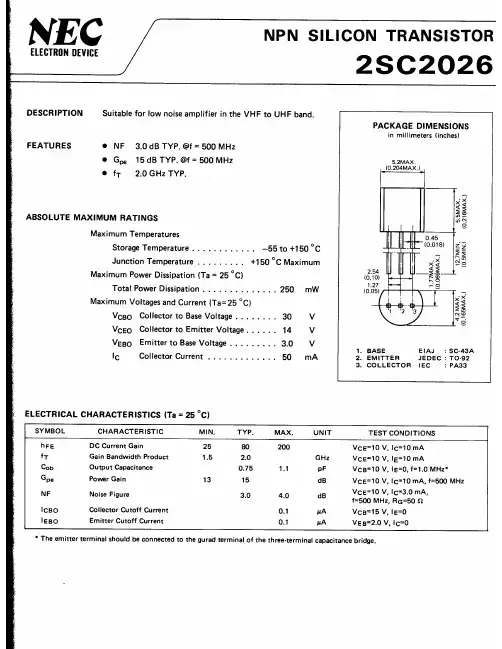

2SC1260 电特性- 参数名称: 2SC1260材料: Si结构: npn最大耗散功率(Pc): 250mW集电极-- 基极击穿电压(Ucb): 45V 集电极-- 发射极击穿电压(Uce): 25V 发射极-- 基极击穿电压(Ueb): 4V最大集电极电流(Ic max): 30mA最高结温 2SC1260 (Tj): 175�C特征频率(ft): 1.5GHz集电极电容(Cc), Pf: 1.4直流电流增益(hFE), min/max: 80T制造商: NEC1.共射极电路当信号与基极偏压同相时,基极电位升高,使基极电流增大,集电极电位降低,集电极负载电流会比基极电流增大量成倍增大;当信号与基极偏压反相时,基极电位降低,使基极电流减小,集电极电位升高,集电极负载电流会比基极电流减小量成倍减小。
集电极电流变化量与三极管放大倍数有关。
共射极电路集电极电位变化方向与基极电位变化方向相反,因此也叫反相器。
信号电流不是直接穿过三极管,只能在基极回路流通,在集电极回路可得到放大的电流信号,这两个回路的公共点是发射极,因此又叫共发射极电路。
共射极电路又称反相放大电路,其特点为电压增益大,输出电压与输入电压反相,低频性能差,适用于低频、和多级放大电路的中间级。
2.共集电极电路共集电极电路又称射极输出器、电压跟随器,其特点是:电压增益小于1而又近似等于1,输出电压与输入电压同相,输入电阻高,输出电阻低,常用于多级放大电路的输入级、输出级或缓冲级。
3 .共基极电路电路特点:输出电压与输入电压同相,输入电阻底,输出电阻高,常用于高频或宽频带电路。
4.反馈是将输出信号的一部分或全部以通过反馈网络送到输入端。
负反馈放大电路有四种不同类型,由瞬时极性判断反馈的性质,由输出端判别电压或电流反馈,由输入端判别串联或并联反馈。
去耦电容在电子电路中,去耦电容和旁路电容都是起到抗干扰的作用,电容所处的位置不同,称呼就不一样了。

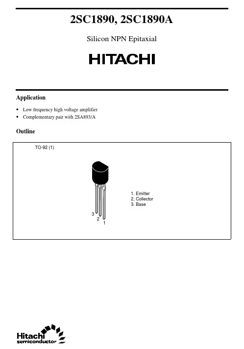
2SC1890, 2SC1890ASilicon NPN EpitaxialApplication• Low frequency high voltage amplifier• Complementary pair with 2SA893/AOutline2SC1890, 2SC1890A2Absolute Maximum Ratings (Ta = 25°C)RatingsItemSymbol 2SC18902SC1890A Unit Collector to base voltage V CBO 90120V Collector to emitter voltage V CEO 90120V Emitter to base voltage V EBO 55V Collector currentI C 5050mA Collector power dissipation P C 300300mW Junction temperature Tj 150150°C Storage temperatureTstg–55 to +150–55 to +150°CElectrical Characteristics (Ta = 25°C)2SC18902SC1890A ItemSymbol Min Typ Max Min Typ Max Unit Test conditions Collector to emitter breakdown voltage V (BR)CEO 90——120——V I C = 1 mA, R BE = ∞Collector cutoff currentI CBO——0.5———µA V CB = 75 V, I E = 0—————0.5µAV CB = 100 V, I E = 0DC current tarnsfer ratio h FE *1250—1200250—1200V CE = 12 V, I C = 2 mA Base to emitter voltage V BE ——0.75——0.75V V CE = 12 V, I C = 2 mA Collector to emitter saturation voltage V CE(sat)——0.5——0.5V I C = 10 mA, I B = 1 mA Gain bandwidth product f T—200——200—MHz V CE = 12 V, I C = 2 mA Collector output capacitance Cob — 1.6—— 1.6—pF V CB = 25 V, I E = 0,f = 1 MHzNoise figure NF—210—210dB V CE = 6 V, I C = 50 µA,R g = 50 k Ω, f = 1 kHzNote: 1.The 2SC1890/A is grouped by h FE as follows.DEF250 to 500400 to 800600 to 1200See characteristic curves of 2SC1775 and 2SC1775A.2SC1890, 2SC1890A3Hitachi CodeJEDECEIAJWeight (reference value)TO-92 (1)ConformsConforms0.25 gUnit: mm元器件交易网Cautions1.Hitachi neither warrants nor grants licenses of any rights of Hitachi’s or any third party’s patent,copyright, trademark, or other intellectual property rights for information contained in this document.Hitachi bears no responsibility for problems that may arise with third party’s rights, includingintellectual property rights, in connection with use of the information contained in this document.2.Products and product specifications may be subject to change without notice. Confirm that you have received the latest product standards or specifications before final design, purchase or use.3.Hitachi makes every attempt to ensure that its products are of high quality and reliability. However,contact Hitachi’s sales office before using the product in an application that demands especially high quality and reliability or where its failure or malfunction may directly threaten human life or cause risk of bodily injury, such as aerospace, aeronautics, nuclear power, combustion control, transportation,traffic, safety equipment or medical equipment for life support.4.Design your application so that the product is used within the ranges guaranteed by Hitachi particularly for maximum rating, operating supply voltage range, heat radiation characteristics, installationconditions and other characteristics. Hitachi bears no responsibility for failure or damage when used beyond the guaranteed ranges. Even within the guaranteed ranges, consider normally foreseeable failure rates or failure modes in semiconductor devices and employ systemic measures such as fail-safes, so that the equipment incorporating Hitachi product does not cause bodily injury, fire or other consequential damage due to operation of the Hitachi product.5.This product is not designed to be radiation resistant.6.No one is permitted to reproduce or duplicate, in any form, the whole or part of this document without written approval from Hitachi.7.Contact Hitachi’s sales office for any questions regarding this document or Hitachi semiconductor products.Hitachi, Ltd.Semiconductor & Integrated Circuits.Nippon Bldg., 2-6-2, Ohte-machi, Chiyoda-ku, Tokyo 100-0004, Japan Tel: Tokyo (03) 3270-2111 Fax: (03) 3270-5109Copyright ' Hitachi, Ltd., 1999. All rights reserved. Printed in Japan.Hitachi Asia Pte. Ltd.16 Collyer Quay #20-00Hitachi TowerSingapore 049318Tel: 535-2100Fax: 535-1533URLNorthAmerica : http:/Europe : /hel/ecg Asia (Singapore): .sg/grp3/sicd/index.htm Asia (Taiwan): /E/Product/SICD_Frame.htm Asia (HongKong): /eng/bo/grp3/index.htm Japan : http://www.hitachi.co.jp/Sicd/indx.htmHitachi Asia Ltd.Taipei Branch Office3F, Hung Kuo Building. No.167, Tun-Hwa North Road, Taipei (105)Tel: <886> (2) 2718-3666Fax: <886> (2) 2718-8180Hitachi Asia (Hong Kong) Ltd.Group III (Electronic Components)7/F., North Tower, World Finance Centre,Harbour City, Canton Road, Tsim Sha Tsui,Kowloon, Hong Kong Tel: <852> (2) 735 9218Fax: <852> (2) 730 0281 Telex: 40815 HITEC HXHitachi Europe Ltd.Electronic Components Group.Whitebrook ParkLower Cookham Road MaidenheadBerkshire SL6 8YA, United Kingdom Tel: <44> (1628) 585000Fax: <44> (1628) 778322Hitachi Europe GmbHElectronic components Group Dornacher Stra§e 3D-85622 Feldkirchen, Munich GermanyTel: <49> (89) 9 9180-0Fax: <49> (89) 9 29 30 00Hitachi Semiconductor (America) Inc.179 East Tasman Drive,San Jose,CA 95134 Tel: <1> (408) 433-1990Fax: <1>(408) 433-0223For further information write to:。
