
AS006L2-00中文资料
- 格式:pdf
- 大小:198.42 KB
- 文档页数:3


AD8331 Evaluation BoardAD8331-EVAL Rev. AInformation furnished by Analog Devices is believed to be accurate and reliable. However, noresponsibility is assumed by Analog Devices for its use, nor for any infringements of patents or other rights of third parties that may result from its use. Specifications subject to change without notice. No license is granted by implication or otherwise under any patent or patent rights of Analog Devices. T rademarks and registered trademarks are the property of their respective owners. O ne Technology Way, P.O. Box 9106, Norwood, MA 02062-9106, U.S.A. Tel: 781.329.4700 Fax: 781.461.3113 ©2006 Analog Devices, Inc. All rights reserved.GENERAL DESCRIPTIONThe AD8331 evaluation board is a platform for testing and evaluating the AD8331 variable gain amplifier (VGA). The board is provided completely assembled and tested; therefore, the user only needs to connect an input signal, V GAIN sources, and a single 5 V power supply.USER SUPPLIED OPTIONAL COMPONENTSAs shown in the schematic in Figure 2 (fixed), the board has provisions for optional components. The basic components are shown in black, and the optional components, which can be installed at the user’s discretion, are shown in grey.The input impedance of the LNA is configured for 50 Ω to accommodate most signal generators and network analyzers. Input impedances up to 6 kΩ can be realized by changing the values of RFB and CSH. Consult the AD8331 data sheet for details on this circuit feature. See Table 1 for typical values of input impedance and corresponding components.Table 1. LNA External Component Values for Common Source ImpedancesR IN (Ω) RFB (Ω, Nearest 1% Value) CSH (pF)50 274 22 75 412 12 100 562 8 200 1.13k1.2 500 3.01k None 6 k ∞ NoneThe board is designed for 0805 size surface-mount components. Space is provided for various popular configurations of overload diodes at locations D1, D2, or D3.The LNA can be evaluated on its own. If so used alone, it mustbe ac-coupled with capacitors at its differential output. Typical values are 0.1 μF, and they are installed at Position C1 and Position C2.Resistors of 0 Ω are installed at R4 and R8, unless capacitive loads larger than 10 pF are connected to the SMA connectors, LON, and LOP (such as coaxial cables.) In that event, small value resistors (68 Ω to 100 Ω) must be installed at R4 and R8.A resistor can be inserted at RCLMP if output clamping is desired. Consult the AD8331 data sheet for appropriate values.4589-1Figure 1. AD8331-EVAL Top ViewThe preferred signal detection method is a differential probe connected to VO, as shown in Figure 3. Single-ended loads can be connected using the board edge SMA connector, VOH. Be sure to take into account the 25.8 dB attenuation incurred when using the board in this manner.MEASUREMENT SETUPThe basic board connection for measuring bandwidth is shown in Figure 3. A 5 V, 100 mA minimum power supply, and a low noise, voltage reference supply for GAIN is required. Table 2 lists jumpers, and Figure 3 shows their function and positions. Table 2. Jumper FunctionsNo. FunctionENBL Enables the LNA when inserted in the top position ENBV Enables the VGA when inserted in the top positionW5, W6 Connects the AD8331’s outputs to the SMA connectors Mode Bottom, gain increases with V GAIN; Top, gain decreases with V GAINHI_LO Top, HI gain; bottom, LO gain (shown in Hi gain position) BOARD LAYOUT AND PARTS LISTThe evaluation board circuitry uses four conductor layers. The two inner layers are grounded, and all interconnecting circuitry is located on the outer layers. Figure 5 to Figure 8 illustrate the copper patterns. Table 3 is a part’s list.AD8331-EVALRev. A | Page 2 of 404589-002NOTES1. COMPONENTS IN GREY ARE OPTIONAL AND USER SUPPLIED.VOHFigure 2. Schematic of Evaluation Board04589-0031103 TEKPROBE POWER SUPPLYDP8200 PRECISION VOLTAGE REFERENCE (FOR VGAIN)4395A ANALYZERGNDFigure 3. Typical Board Test ConnectionsAD8331-EVALRev. A | Page 3 of 404589-004Figure 4. Top Silkscreen04589-005Figure 5. Primary Side Copper04589-006Figure 6. Secondary Side Copper04589-007Figure 7. Internal Layer GroundFigure 8. Power PlaneAD8331-EVALRev. A | Page 4 of 4Table 3. Parts ListQty Name DescriptionReference Designation Mfg. Mfg. Part Number 5 Inductors Ferrite Bead, 120 nH, 0603 L1, L2, L3, L4, L5 Murata BLM18BA750SN1D 1 Resistor SM, 274 Ω, 1%, 1/10 W, 0603 RFB Panasonic ERJ-3EKF2740V 2 Resistors SM, 237 Ω, 1%, 1/10 W, 0603 R16, R20 Panasonic ERJ-3EKF2370V 2 Resistors SM, 100 Ω, 1%, 1/10 W, 0603 R43, R44 Panasonic ERJ-3EKF1 1 Capacitor 0.018 μF, 10%, X7R, 0603 CFBPanasonicECJ-1VB1E183K10Capacitor0.1 μF, 50 V, 0603 C6, C14, C16, C18, C24, C26, C32, C35, C INH , CLMD Kemet C0603C104K4RAC 1 Capacitor 1000 pF, 50 V, 0603 C34 Panasonic ECJ-1VB2A102K 1 Capacitor 10 μF, 10V Tantalum C3Nichicon F931A106MAA 6 Shunt ShuntHI_LO (HI), MODE (UP),ENBL (EN), ENBV (EN), W5, W6 W. M. Berg65474-0011 Capacitor 22 pF, 50 V, 0603CSH Panasonic ECJ-1VC1H220J 1 Transformer RF, 0.015 MHz to 300 MHz T1Mini-Circuit #T1-6T KK814 Bumper FootUsed as feet. Mount to wiring side of board at 4 corners 3M S J -67A11 1 Integrated Circuit Variable Gain Amplifier DUTAnalog Devices, Inc. AD8331ARQ 3 Connector 2-Pin Header VO, W5, W6W. M. Berg 69157-102 4 Connector 3-Pin HeaderENBL, ENBV, HI_LO, MODE Fixed Molex 22-11-2032 2 Connectors SMA, Right Angle PC Mount INH, VOH Amphenol 901-143-6RFX 1 Test Point Red Loop +5VBisco TP-104-01-02 5 Test Points Black Loop GND, GND 1, GND 2, GND 3, GND 4 Bisco TP-104-01-001Test PointsPurple LoopVCM FixedBisco TP-104-01-07ESD CAUTIONESD (electrostatic discharge) sensitive device. Electrostatic charges as high as 4000 V readily accumulate on the human body and test equipment and can discharge without detection. Although this product features proprietary ESD protection circuitry, permanent damage may occur on devices subjected to high energy electrostatic discharges. Therefore, proper ESD precautions are recommended to avoid performance degradation or loss of functionality.ORDERING GUIDEModel Description AD8331-EVAL Evaluation Board with AD8331ARQ©2006 Analog Devices, Inc. All rights reserved. Trademarks and registered trademarks are the property of their respective owners. D04589-0-4/06(A)。
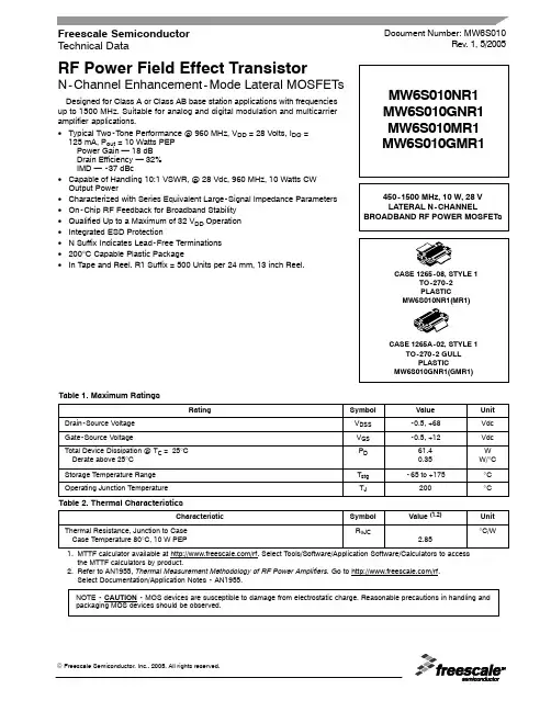
RF Power Field Effect TransistorN-Channel Enhancement-Mode Lateral MOSFETsDesigned for Class A or Class AB base station applications with frequenciesup to 1500 MHz. Suitable for analog and digital modulation and multicarrieramplifier applications.•Typical Two-Tone Performance @ 960 MHz, V DD = 28 Volts, I DQ =125 mA, P out = 10 Watts PEPPower Gain — 18 dBDrain Efficiency — 32%IMD — -37 dBc•Capable of Handling 10:1 VSWR, @ 28 Vdc, 960 MHz, 10 Watts CWOutput Power•Characterized with Series Equivalent Large-Signal Impedance Parameters•On-Chip RF Feedback for Broadband Stability•Qualified Up to a Maximum of 32 V DD Operation•Integrated ESD Protection•N Suffix Indicates Lead-Free Terminations•200°C Capable Plastic Package•In Tape and Reel. R1 Suffix = 500 Units per 24 mm, 13 inch Reel.Table 1. Maximum RatingsRating Symbol Value Unit Drain-Source Voltage V DSS-0.5, +68Vdc Gate-Source Voltage V GS-0.5, +12Vdc Total Device Dissipation @ T C = 25°CDerate above 25°CP D61.40.35WW/°C Storage Temperature Range T stg-65 to +175°C Operating Junction Temperature T J200°C Table 2. Thermal CharacteristicsCharacteristic Symbol Value (1.2)Unit Thermal Resistance, Junction to CaseCase Temperature 80°C, 10 W PEPRθJC2.85°C/W1.MTTF calculator available at /rf. Select Tools/Software/Application Software/Calculators to accessthe MTTF calculators by product.2.Refer to AN1955, Thermal Measurement Methodology of RF Power Amplifiers. Go to /rf.Select Documentation/Application Notes - AN1955.Document Number: MW6S010Rev. 1, 5/2005 Freescale SemiconductorTechnical Data2RF Device DataFreescale SemiconductorMW6S010NR1 MW6S010GNR1 MW6S010MR1 MW6S010GMR1Table 3. ESD Protection CharacteristicsTest MethodologyClass Human Body Model (per JESD22-A114)1A Machine Model (per EIA/JESD22-A115)A Charge Device Model (per JESD22-C101)IIITable 4. Moisture Sensitivity LevelTest MethodologyRating Package Peak TemperatureUnit Per JESD 22-A113, IPC/JEDEC J-STD-0201260°CTable 5. Electrical Characteristics (T C = 25°C unless otherwise noted)CharacteristicSymbolMinTypMaxUnitOff CharacteristicsZero Gate Voltage Drain Leakage Current (V DS = 68 Vdc, V GS = 0 Vdc)I DSS ——10µAdc Zero Gate Voltage Drain Leakage Current (V DS = 28 Vdc, V GS = 0 Vdc)I DSS ——1µAdc Gate-Source Leakage Current (V GS = 5 Vdc, V DS = 0 Vdc)I GSS——1µAdcOn CharacteristicsGate Threshold Voltage(V DS = 10 Vdc, I D = 100 µAdc)V GS(th) 1.5 2.33Vdc Gate Quiescent Voltage(V DS = 28 Vdc, I D = 125 mAdc)V GS(Q)— 3.1—Vdc Drain-Source On-Voltage(V GS = 10 Vdc, I D = 0.3 Adc)V DS(on)—0.270.35VdcDynamic CharacteristicsInput Capacitance(V DS = 28 Vdc ± 30 mV(rms)ac @ 1 MHz, V GS = 0 Vdc)C iss —23—pF Output Capacitance(V DS = 28 Vdc ± 30 mV(rms)ac @ 1 MHz, V GS = 0 Vdc)C oss —10—pF Reverse Transfer Capacitance(V DS = 28 Vdc ± 30 mV(rms)ac @ 1 MHz, V GS = 0 Vdc)C rss—0.32—pFFunctional Tests (In Freescale Test Fixture, 50 ohm system) V DD = 28 Vdc, I DQ = 125 mA, P out = 10 W PEP , f = 960 MHz, Two-Tone Test, 100 kHz Tone Spacing Power Gain G ps 17.51820.5dB Drain EfficiencyηD 3132—%Intermodulation Distortion IMD —-37-33dBc Input Return LossIRL—-18-10dBTypical Performances (In Freescale 450 MHz Demo Board, 50 οhm system) V DD = 28 Vdc, I DQ = 150 mA, P out = 10 W PEP , 420 MHz<Frequency<470 MHz, Two-Tone Test, 100 kHz Tone Spacing Power Gain G ps —20—dB Drain EfficiencyηD —33—%Intermodulation Distortion IMD —-40—dBc Input Return LossIRL—-10—dBMW6S010NR1 MW6S010GNR1 MW6S010MR1 MW6S010GMR13RF Device DataFreescale SemiconductorFigure 1. MW6S010NR1(GNR1/MR1/GMR1) Test Circuit Schematic — 900 MHzZ50.313″ x 0.902″ Microstrip Z60.073″ x 1.080″ Microstrip Z70.073″ x 0.314″ MicrostripPCBRogers ULTRALAM 2000, 0.031″, εr = 2.55Z10.073″ x 0.223″ Microstrip Z20.112″ x 0.070″ Microstrip Z30.213″ x 0.500″ Microstrip Z40.313″ x 1.503″ Microstrip Table 6. MW6S010NR1(GNR1/MR1/GMR1) Test Circuit Component Designations and Values — 900 MHzPartDescriptionPart Number Manufacturer B1Ferrite Bead2743019447Fair-Rite C1, C6, C11, C2047 pF Chip Capacitors100B470JP500X ATC C2, C18, C1922 µF, 35 V Tantalum CapacitorsT491D226K035AS Kemet C3, C16220 µF, 63 V Electrolytic Capacitors, Radial 13668221Phillips C4, C150.1 µF Chip CapacitorsCDR33BX104AKWS Kemet C5, C8, C170.8-8.0 pF Variable Capacitors, Gigatrim 272915L Johanson C7, C1224 pF Chip Capacitors 100B240JP500X ATC C9, C10, C13 6.8 pF Chip Capacitors 100B6R8JP500X ATC C147.5 pF Chip Capacitor 100B7R5JP500X ATC L112.5 nH Inductor A04T-5Coilcraft R11 k Ω Chip ResistorCRCW12061001F100Vishay -Dale4RF Device DataFreescale SemiconductorMW6S010NR1 MW6S010GNR1 MW6S010MR1 MW6S010GMR1Figure 2. MW6S010NR1(GNR1/MR1/GMR1) Test Circuit Component Layout — 900 MHzMW6S010NR1 MW6S010GNR1 MW6S010MR1 MW6S010GMR15RF Device DataFreescale SemiconductorTYPICAL CHARACTERISTICS — 900 MHzP out , OUTPUT POWER (WATTS) AVG.1520119171610100Figure 4. Two-Tone Power Gain versusOutput Power1000.1110P out , OUTPUT POWER (WATTS) AVG.Figure 5. Intermodulation Distortion Productsversus Output PowerG p s , P O W E R G A I N (d B )10−55−150.1TWO−TONE SPACING (MHz)−20−25−30−35−401100Figure 6. Intermodulation Distortion Productsversus Tone Spacing 2948P in , INPUT POWER (dBm)46444240382123252719Figure 7. Pulse CW Output Power versusInput PowerI M D , I N T E R M O D U L A T I O N D I S T O R T I O N (d B c )P o u t , O U T P U T P O W E R (d B m )18−50−450.16RF Device DataFreescale SemiconductorMW6S010NR1 MW6S010GNR1 MW6S010MR1 MW6S010GMR1TYPICAL CHARACTERISTICS — 900 MHzA C P R (dB c )0−60P out , OUTPUT POWER (WATTS) AVG.50−1040−2030−3020−4010−500.1110Figure 8. Single-Carrier CDMA ACPR, PowerGain and Power Added Efficiencyversus Output PowerP out , OUTPUT POWER (WATTS) CWFigure 10. Power Gain versus Output Power 14151912171618468G p s , P O W E R G A I N (d B )500−255f, FREQUENCY (MHz)Figure 11. Broadband Frequency Response−5−10−15−20120011001000900800700600S 11 (d B )16102ηD , D R A I N E F F I C I E N C Y (%), G p s , P O W E R G A I N (d B )MW6S010NR1 MW6S010GNR1 MW6S010MR1 MW6S010GMR17RF Device DataFreescale SemiconductorTYPICAL CHARACTERISTICS21010890T J , JUNCTION TEMPERATURE (°C)Figure 12. MTTF Factor versus Junction TemperatureThis above graph displays calculated MTTF in hours x ampere 2drain current. Life tests at elevated temperatures have correlated to better than ±10% of the theoretical prediction for metal failure. Divide MTTF factor by I D 2 for MTTF in a particular application.107106105120140160180190M T T F F A C T O R (H O U R S x A M P S 2)1002001701501301108RF Device DataFreescale SemiconductorMW6S010NR1 MW6S010GNR1 MW6S010MR1 MW6S010GMR1f MHz Z sourceΩZ load Ω800820840 3.1 + j1.92.7 + j2.22.8 + j1.710.1 + j2.38.3 + j2.58.2 + j3.3V DD = 28 Vdc, I DQ = 125 mA, P out = 10 W PEP 860880900 3.1 + j3.42.9 + j3.73.3 + j3.89.8 + j4.810.6 + j5.69.5 + j5.5920940960 2.8 + j4.43.2 + j4.93.0 + j4.710.1 + j5.911.0 + j6.411.8 + j6.69803.6 + j5.212.1 + j7.1Figure 13. Series Equivalent Source and Load Impedance — 900 MHzZ source =Test circuit impedance as measured fromgate to ground.Z load=Test circuit impedance as measured from drain to ground.ZsourceZloadOutput Matching Networkf = 800 MHzf = 980 MHzZ o = 25 Ωf = 800 MHzf = 980 MHzZ loadZ sourceMW6S010NR1 MW6S010GNR1 MW6S010MR1 MW6S010GMR19RF Device DataFreescale SemiconductorFigure 14. MW6S010NR1(GNR1/MR1/GMR1) Test Circuit Schematic — 450 MHzZ50.475″ x 0.330″ Microstrip Z60.475″ x 0.325″ Microstrip Z8 1.250″ x 0.080″ MicrostripPCBRogers ULTRALAM 2000, 0.030″, εr = 2.55Z10.540″ x 0.080″ Microstrip Z20.365″ x 0.080″ Microstrip Z30.225″ x 0.080″ Microstrip Z4, Z70.440″ x 0.080″ Microstrip R3R4Table 7. MW6S010NR1(GNR1/MR1/GMR1) Test Circuit Component Designations and Values — 450 MHzPartDescriptionPart Number Manufacturer B1, B2Ferrite Bead2743019447Fair-Rite C1 1 µF, 35 V Tantalum Capacitor T491C105K050AS Kemet C2, C1522 µF, 35 V Tantalum Capacitors T491X226K035AS Kemet C3, C140.1 µF Chip Capacitors C1210C104K5RACTR Kemet C4, C9, C10, C13330 pF Chip Capacitors 700A331JP150X ATC C5 4.3 pF Chip Capacitor 100B4R3JP500X ATC C6, C110.6-8.0 pF Variable Capacitors 27291SL Johanson C7, C8, C12 4.7 pF Chip Capacitors 100B4R7JP500X ATC L139 µH Chip Inductor ISC-1210Vishay -Dale R110 Ω Chip Resistor (0805)CRCW080510R0F100Vishay -Dale R2 1 k Ω Chip Resistor (0805)CRCW08051001F100Vishay -Dale R3 1.2 k Ω Chip Resistor (0805)CRCW08051201F100Vishay -Dale R4 2.2 k Ω Chip Resistor (0805)CRCW08052201F100Vishay -Dale R5 5 k Ω Potentiometer 1224WBourns R6 1 k Ω Chip Resistor (1206)CRCW12061001F100Vishay -Dale T1 5 Volt Regulator, Micro 8LP2951On Semiconductor T2NPN TransistorBC847ALT1On Semiconductor10RF Device DataFreescale SemiconductorMW6S010NR1 MW6S010GNR1 MW6S010MR1 MW6S010GMR1Figure 15. MW6S010NR1(GNR1/MR1/GMR1) Test Circuit Component Layout — 450 MHzMW6S010NR1 MW6S010GNR1 MW6S010MR1 MW6S010GMR111RF Device DataFreescale SemiconductorTYPICAL CHARACTERISTICS — 450 MHzI R L , I N P U T R E T U R N L O S S (d B )A C P R (dB c ), A L T 1 (d B c )500400f, FREQUENCY (MHz)Figure 16. 2-Carrier W-CDMA Broadband Performance @ P out = 3 Watts Avg.−21−6−9−12−1518.420.4−6537343128−40−45−50−55ηD , D R AI N E F F I C I E N C Y (%)G p s , P O W E R G A IN (d B )25−60−1820.22019.819.619.419.21918.818.6410420430440450460470480490f, FREQUENCY (MHz)Figure 17. 2-Carrier W-CDMA Broadband Performance @ P out = 7.5 Watts Avg.−50I R L , I N P U T R E T U R N L O S S (d B )A C P R (d B c ), A L T 1 (d B c )500400−14−4−6−8−1016.519−5555504540−30−35−40−45ηD , D R A I N E F F I C I E N C Y (%)G p s , P O W E R G A I N (d B )35−1218.818.518.31817.817.517.31716.8410420430440450460470480490f, FREQUENCY (MHz)Figure 18. Broadband Frequency Response65050530−250−5−15−20S 11S 21−1025201510100150200250300350400450500550600Figure 19. Single-Carrier N-CDMA ACPR, ALT1and ALT2 versus Output Power−80P out , OUTPUT POWER (WATTS) AVG.−10−20−30−40−700.1110−50A L T 1 & A L T 2, C H A N N E L P O W E R (d B c )A C P R , A D J A C E N T C H A N N E L P O W E R R A T I O (dB c )−6012RF Device DataFreescale SemiconductorMW6S010NR1 MW6S010GNR1 MW6S010MR1 MW6S010GMR1f MHz Z sourceΩZ load Ω4004204409.0 + j3.89.6 + j6.68.8 + j5.415.0 + j1.414.3 + j3.315.0 + j4.7V DD = 28 Vdc, I DQ = 150 mA, P out= 10 W PEP 46048050010.6 + j9.511.5 + j13.910.7 + j12.616.3 + j7.316.4 + j11.116.9 + j12.7Figure 20. Series Equivalent Source and Load Impedance — 450 MHzZ source =Test circuit impedance as measured fromgate to ground.Z load=Test circuit impedance as measured from drain to ground.ZsourceZloadOutput Matching Networkf = 400 MHzZ o = 25 ΩZ loadZ sourcef = 500 MHzf = 400 MHzf = 500 MHzMW6S010NR1 MW6S010GNR1 MW6S010MR1 MW6S010GMR113RF Device DataFreescale SemiconductorNOTES14RF Device DataFreescale SemiconductorMW6S010NR1 MW6S010GNR1 MW6S010MR1 MW6S010GMR1PACKAGE DIMENSIONSTO-270-2PLASTICCASE 1265-08ISSUE GMW6S010NR1(MR1)MW6S010NR1 MW6S010GNR1 MW6S010MR1 MW6S010GMR115RF Device DataFreescale SemiconductorTO-270-2 GULLPLASTICCASE 1265A-02ISSUE A BOTTOM VIEWPIN 1.DRAIN 2.GATE 3.SOURCEMW6S010GNR1(GMR1)Information in this document is provided solely to enable system and softwareimplementers to use Freescale Semiconductor products. There are no express orimplied copyright licenses granted hereunder to design or fabricate any integratedcircuits or integrated circuits based on the information in this document.Freescale Semiconductor reserves the right to make changes without further notice toany products herein. Freescale Semiconductor makes no warranty, representation orguarantee regarding the suitability of its products for any particular purpose, nor doesFreescale Semiconductor assume any liability arising out of the application or use ofany product or circuit, and specifically disclaims any and all liability, including withoutlimitation consequential or incidental damages. “Typical” parameters that may beprovided in Freescale Semiconductor data sheets and/or specifications can and dovary in different applications and actual performance may vary over time. All operatingparameters, including “Typicals”, must be validated for each customer application bycustomer’s technical experts. Freescale Semiconductor does not convey any licenseunder its patent rights nor the rights of others. Freescale Semiconductor products arenot designed, intended, or authorized for use as components in systems intended forsurgical implant into the body, or other applications intended to support or sustain life,or for any other application in which the failure of the Freescale Semiconductor productcould create a situation where personal injury or death may occur. Should Buyerpurchase or use Freescale Semiconductor products for any such unintended orunauthorized application, Buyer shall indemnify and hold Freescale Semiconductorand its officers, employees, subsidiaries, affiliates, and distributors harmless against allclaims, costs, damages, and expenses, and reasonable attorney fees arising out of,directly or indirectly, any claim of personal injury or death associated with suchunintended or unauthorized use, even if such claim alleges that FreescaleSemiconductor was negligent regarding the design or manufacture of the part.Freescale t and the Freescale logo are trademarks of Freescale Semiconductor, Inc.All other product or service names are the property of their respective owners.Freescale Semiconductor, Inc. 2005. All rights reserved.How to Reach Us:Home Page:E-mail:support@USA/Europe or Locations Not Listed:Freescale SemiconductorTechnical Information Center, CH3701300 N. Alma School RoadChandler, Arizona 85224+1-800-521-6274 or +1-480-768-2130support@Europe, Middle East, and Africa:Freescale Halbleiter Deutschland GmbHTechnical Information CenterSchatzbogen 781829 Muenchen, Germany+44 1296 380 456 (English)+46 8 52200080 (English)+49 89 92103 559 (German)+33 1 69 35 48 48 (French)support@Japan:Freescale Semiconductor Japan Ltd.HeadquartersARCO Tower 15F1-8-1, Shimo-Meguro, Meguro-ku,Tokyo 153-0064Japan0120 191014 or +81 3 5437 9125support.japan@Asia/Pacific:Freescale Semiconductor Hong Kong Ltd.Technical Information Center2 Dai King StreetTai Po Industrial EstateTai Po, N.T., Hong Kong+800 2666 8080@For Literature Requests Only:Freescale Semiconductor Literature Distribution CenterP.O. Box 5405Denver, Colorado 802171-800-441-2447 or 303-675-2140Fax: 303-675-2150LDCForFreescaleSemiconductor@。