
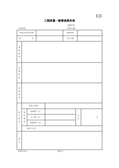
A-14
- 格式:doc
- 大小:24.00 KB
- 文档页数:1
Unit 14 What colour is your T-shirt?●音标:ee在单词中的发音●重点词汇:anorak cap T-shirt shirt sweater●新课标词汇:cap T-shirt shirt sweatercap:字母c, ap的基本发音,大小写书写,以及单词的发音和书写。
T-shirt:字母ir, t的基本发音,复习sh的发音,让学生说出一些含有sh的单词,或者给出一些生词让学生拼读(如:shape),大小写书写,以及单词的发音和书写。
shirt:字母sh, ir, t的基本发音,大小写书写,以及单词的发音和书写,与T-shirt结合记忆。
建议:可以通过图片和班上学生穿着的衣物来引出单词。
可就学生穿着的衣物适当补充教授:coat, jacket通过自然拼音教授和操练单词,操练时可以让学生指着自己或同伴的衣服说:It's a ___.。
●课文重点:1)、What colour is your T-shirt?It's red.先复习颜色单词,再让学生运用句型"My / His / Her / Your coat is red"这类句型来介绍自己和同伴穿着的衣物的颜色,已达到操练答句的作用。
然后再加入老师的提问:What colour is your/ his / her / my ____. 注意复习colour的发音和拼写。
可以进行小组的对话表演。
●重点语法:1)、复习形容词性物主代词:my, his, her, its, your加强对这些代词的认识,提高运用能力,熟练地运用于描述衣物的颜色中。
2)、What colour is it? It's red.学生更够用it来指代某一个物品,如My T-shirt is red. 可以指着实物或图片说:It is red. 缩写成:It's red. 问句中同样可以进行替代,如:What colour is your T-shirt? 可以指着实物或图片说:What colour is it?让学生在有实物或图片的情况下运用个句型。

04使用向导感谢您购买本产品!无刷动力系统功率强大,错误的使用可能导致人身伤害或者设备损坏,为此我们强烈建议您在使用设备前仔细阅读本说明书,并严格遵守规定的操作程序。
我们不承担因使用本产品或擅自对产品进行改造所引起的任何责任,包括但不限于对附带03产品规格警告!电调默认开启DEO功能时收油门具有刹车效果和反串电压,请勿使用不能吸收反串电压的电源设备进行电调测试,否则会损坏电调和电源。
05正常开机过程将系统接上电池,马达发出鸣叫“♪123”,表示动力系统准备就绪,自检结束,随时可以起飞。
01注意事项02产品特色·电调与相关部件连接前,请确保所有接触端绝缘良好,短路会毁坏电调。
·请务必仔细连接好各部件,若接触不良,您可能无法正常控制飞行器,或出现设备损坏等其他不可预知的情况。
·使用此电调前,请认真查看电调以及电机说明书,确保动力系统搭配合理,避免错误的搭配导致损害电调。
·若需对电调的输入、输出线插头做相关焊接,请保证焊接牢靠,并使用足功率的焊接设备。
·勿使电调外部环境温度超过65℃,高温将会毁坏电调并且可能导致电机损害造成炸机。
·若需改变电机工作时的转向,可更改任意两根相线次序。
·本电调拥有CAN功能,在使用CAN功能时,同一架飞机,电调ID和油门通道不能相同,否则多电调会被识别为同一个。
·电调出厂默认不带CAN终端电阻,需整机进行统一匹配。
·多旋翼专用核心程序,油门响应速度大幅提升。
·内置存储芯片,实时记录电调运行数据,具备黑匣子功能。
本电调采用纳米镀膜工艺,防护等级IP55,可定制IP67。
·微处理器采用独立的稳压IC供电,具有更好的抗干扰能力,大幅度降低失控的可能性。
·使用屏蔽线,提升抗干扰能力,屏蔽外界和自身干扰,保证信号质量。
·BLDC方波驱动技术,兼容性好,一个程序可兼容多款电机。

Unit14 I remember meeting all of you in Grade 7.SectionA (1a-2d)I. 单项选择:(BC层学生必做,A层选做或不做)( )1. ---Do you still remember _________with Yao Ming in Beijing?---Yes, of course. Two years ago.\A. to meetB. meetingC. meetD. met( )2. Mr. Green, a famous writer, ___________our school next week.A. visitedB. visitsC. was visitingD. will visit ( )3. ---I feel so sad. My writing is terrible.---Don’t worry. ___________A. It’s not serious!B. It takes time!C. Me, too!D. Sounds funny! ( )4. You’d better read the _________ first before you use the camera.A. websitesB. expressionsC. instructionsD. advertisements ( )5. A student in Fudan University was killed by his roomates just because of small things in daily life. It is important for students to learn how to __________ others.A. get on withB. come over toC. stay away fromD. catch up with ( )6. Please remember ___________your notebook here tomorrow.A. bringsB. broughtC. bringingD. to bring ( )7. Kate’s dad is getting old. She will go back home to see him _______ it is convenient.A. becauseB. wheneverC. althoughD. unless( )8. All the teachers advise me ________ harder.A. workB. to workC. workedD. working ( )9. ---What did Mr. Green say to his son?---He told him _________.A. didn’t smokeB. don’t smokeC. not to smokeD. not smoke ( )10. My father always _____me when I am upset.A. encourageB. guideC. enjoysD. doubleII. 根据句意、首字母及汉语提示补全单词。
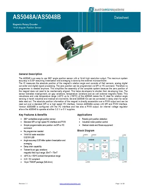
General DescriptionThe AS5048 is an easy to use 360° angle position sensor with a 14-bit high resolution output. The maximum system accuracy is 0.05° assuming linearization and averaging is done by the external microcontroller.The IC measures the absolute position of the magnet’s rotation angle and consists of Hall sensors, analog digital converter and digital signal processing. The zero position can be programmed via SPI or I²C command. Therefore no programmer is needed anymore. This simplifies the assembly of the complete system because the zero position of the magnet does not need to be mechanically aligned. This helps developers to shorten their developing time. The sensor tolerates misalignment, air gap variations, temperature variations and as well external magnetic fields. This robustness and wide temperature range (-40°C up to +150°C) of the AS5048 makes the IC ideal for rotation angle sensing in harsh industrial and medical environments. Several AS5048 ICs can be connected in daisy chain for serial data read out. The absolute position information of the magnet is directly accessible over a PWM output and can be read out over a standard SPI or a high speed I²C interface. Version AS5048A comes with SPI and PWM Interface. Version AS5048B is configured with the I²C interface and has also a PWM output. An internal voltage regulator allows the AS5048 to operate at either 3.3 V or 5 V supplies.Key Features & Benefits • 360° contactless angle position sensor• Standard SPI or high speed I²C interface and PWM • Simple programmable zero position via SPI or I²C command• No programmer needed • 14-bit full scale resolution 0.0219°/LSB• Angle accuracy 0.05°after system linearization and averaging• Daisy chain capability• Tolerant to air gap variationsmagnetic field input range: 30mT – 70mT • -40°C to +150°C ambient temperature range • 3.3V / 5V compliant• 14-pin TSSOP package (5x6.4mm)Applications• Robotic joint position detection • Industrial motor position control• Medical robots and fitness equipmentBlock DiagramContentsGENERAL DESCRIPTION (1)K EY F EATURES &B ENEFITS (1)A PPLICATIONS (1)B LOCK D IAGRAM (1)1PIN CONFIGURATION (4)1.1P IN D ESCRIPTION (4)2ELECTRICAL CHARACTERISTICS (5)2.1A BSOLUTE M AXIMUM R ATINGS (5)2.2O PERATING C ONDITIONS (6)2.3DC/AC C HARACTERISTICS FOR DIGITAL INPUTS AND OUTPUTS (6)2.4E LECTRICAL S YSTEM S PECIFICATIONS (7)2.5G LOBAL T IMING C ONDITIONS (7)3FUNCTIONAL DESCRIPTION (8)4OPERATION (8)4.1SPI I NTERFACE (9)4.1.1SPI Interface Signals (4-Wire Mode, Wire_mode = 1) (9)4.1.2SPI Timing (10)4.1.3SPI Connection to the Host UC (11)4.1.4SPI Communication Command Package (12)4.1.5Read Package (Value Read from AS5048A) (13)4.1.6Write Data Package (Value Written to AS5048A) (13)4.1.7Register Map SPI (14)4.1.8SPI Interface Commands (15)4.2I²C INTERFACE (18)4.2.1I²C Electrical Specification (18)4.2.2I²C Timing (19)4.2.3Register Table (20)4.3PWM INTERFACE (21)5PACKAGE DRAWINGS AND MARKINGS (22)5.1.1Assembly Lot Code (22)6APPLICATION INFORMATION (24)6.1P ROGRAMMING OF THE AS5048 (24)6.1.1Programming of the zero position (24)6.1.2Programming sequence with verification (24)6.2D IAGNOSTIC FUNCTIONS OF THE AS5048 (24)6.3C HOOSING THE P ROPER M AGNET (25)6.4P HYSICAL P LACEMENT OF THE M AGNET (26)6.5M AGNET P LACEMENT (26)7ORDERING INFORMATION (27)8REVISION HISTORY (27)9COPYRIGHTS (28)10DISCLAIMER (28)List of FiguresF IGURE 1:P IN CONFIGURATION TSSOP14 (4)F IGURE 2:C ONNECTIONS FOR 5V AND 3.3V SUPPLY VOLTAGES (8)F IGURE 3SPI C ONNECTION AS5048A WITH U C (9)F IGURE 4SPI C OMMAND/R ESPONSE D ATA F LOW (9)F IGURE 5SPI T IMING D IAGRAM (10)F IGURE 6S INGLE S LAVE M ODE (11)F IGURE 7M ULTIPLE S LAVE, N+3W IRE (S EPARATE C HIP S ELECT) (11)F IGURE 8D AISY C HAIN,4W IRE (12)F IGURE 9READ C OMMAND (15)F IGURE 10WRITE C OMMAND (15)F IGURE 11CLEAR ERROR FLAG C OMMAND (16)F IGURE 12NOP C OMMAND (17)F IGURE 13PWM F ORMAT (21)F IGURE 14P ACKAGE M ARKING (22)F IGURE 15:T YPICAL MAGNET (6X3MM) AND MAGNETIC FIELD DISTRIBUTION (25)F IGURE 16:D EFINED CHIP CENTER AND MAGNET DISPLACEMENT RADIUS (26)F IGURE 17:V ERTICAL PLACEMENT OF THE MAGNET (26)List of TablesT ABLE 1:P IN DESCRIPTION TSSOP14 (4)T ABLE 2A BSOLUTE M AXIMUM R ATINGS (5)T ABLE 3:O PERATING C ONDITION (6)T ABLE 4:DC/AC CHARACTERISTICS (6)T ABLE 5S YSTEM SPECIFICATION (7)T ABLE 6G LOBAL TIMING CONDITIONS (7)T ABLE 7SPI T IMING C HARACTERISTICS (10)T ABLE 8SPI C OMMAND P ACKAGE (12)T ABLE 9SPI READ PACKAGE (13)T ABLE 10SPI WRITE DATA PACKAGE (13)T ABLE 11SPI REGISTER MAP (14)T ABLE 12C LEAR E RROR F LAG C OMMAND (16)T ABLE 13NOP C OMMAND (17)T ABLE 14I²C E LECTICAL S PECIFICATION (18)T ABLE 15 I²C T IMING ............................................................................................................................ 19 T ABLE 16 R EGISTER M AP I2C ................................................................................................................ 20 T ABLE 17 PWM P ERIOD AND RESOLUTION .............................................................................................. 21 T ABLE 18: O RDERING I NFORMATION (27)1 Pin Configuration2345678910111213141SDA/CSn SCL/CLK A2/MISO A1/MOSI TEST TEST TESTTESTTEST TEST VDD5V VDD3V GND PWM AS5048Figure 1: Pin configuration TSSOP141.1 Pin DescriptionPin Symbol Type Description1 SDA/CSn DI_ST SPI chip select - active low; shared with I2C chip select pin2 SCL/CLK DI_ST SPI clock input; shared with I2C clock input3 A2/MISO DIO_ST SPI master in/slave out; shared with I2C address selection pin 24 A1/MOSI DI_ST SPI master out/slave in; shared with I2C address selection pin 15 TEST AIO Test pin, see Note6 TEST AIO Test pin, see Note7 TEST AIO Test pin, see Note8 TEST AIO Test pin, see Note9 TEST AIO Test pin, see Note 10 TEST AIO Test pin, see Note11 VDD5V S Positive Supply Voltage, 3.0 to 5.5 V12VDD3VS3.3V Regulator output; internally regulated from VDD. Connect to VDD for 3V supply voltage. 10uF capacitor to GND required in 5V operation mode13 GND S Negative Supply Voltage (GND) 14PWMDOPulse Width Modulation outputTable 1: Pin description TSSOP14PIN Types: S ... supply pad AIO ... analog I/O DI_ST … digital input with schmitt trigger DO ... digital output – push-pull DIO _ST ... digital I/O with schmitt trigger in the input pathNote: Pin 5 should be grounded to VSS. Pins 6, 7, 8, 9, 10 should be left open during the normal operation.2Electrical Characteristics2.1Absolute Maximum RatingsStresses beyond those listed under “Absolute Maximum Ratings“ may cause permanent damage to the device. These are stress ratings only. Functional operation of the device at these or any other conditions beyond those indicated under “Operating Conditions” is not implied. Exposure to absolute maximum rating conditions for extended periods may affect device reliability.Parameter Symbol Min Max Unit NoteDC supply voltage at VDD pin VDD5V -0.3 7 V (1)DC voltage at VDD3V pin VDD3V -0.3 5 VDC voltage at GND pin GND -0.3 0.3 VInput pin voltage V_in VDD+0.3 VInput current (latchup immunity) I_scr -100 100 mA Norm: Jedec 78Electrostatic discharge ESD +/-2 kV Norm: MIL 883 E method 3015Total power dissipation (all supplies andoutputs)P_t 150 mWStorage temperature T_strg -55 150 °CPackage body temperature T_body 260 °C The reflow peak soldering temperature (body temperature)specified is in accordance with IPC/JEDEC J-STD-020 “Moisture Solid State Surface Mount Devices”. The lead finish from Pb-free leaded packages is matte tin (100% Sn)Humidity non-condensing H 5 85 %Moisture Sensitive Level MSL 3 Represents a maximum floor life time of 168hTable 2 Absolute Maximum Ratings2.2Operating ConditionsAll in this specification defined tolerances for external components need to be assured over the whole operation conditions range and also over lifetime.Parameter Symbol Min Max Unit NotePositive supply voltage VDD5V 4.5 5.5 V 5V Operation via LDOVDD3V 3 3.6 V LDO output voltage Positive core supply voltage VDDCORE 3 3.6 VNegative supply voltage GND 0 0 VAmbient temperature T_amb -40 150 °C Only for 5V operation.T_amb_max for 3V is 125°C Supply Current I_sup 15 mATable 3: Operating Condition2.3DC/AC Characteristics for digital inputs and outputsParameter Symbol Min Typ Max Unit Note CMOS digital input with schmitt trigger: CSn, CLK, MOSIHigh level input voltage V_IH 0.7 * VDD5V VLow level input voltage V_IL 0.3 * VDD5V VInput leakage current l_LEAK 1 µACMOS output: PWM, MISOHigh level output voltage V_OH VDD5V-0.5 VLow level output voltage V_OL GND+0.4 VCapacitive load C_L 50 pFOutput current I_OUT 4 mATable 4:DC/AC characteristics2.4Electrical System SpecificationsVDD5V = 5V, T Ambient = -40 to +150°C unless noted otherwiseParameter Symbol Min Typ Max Unit Note Magnetic input field Bz 30 50 70 mTOutput sampling rate f sample10.2 11.25 12.4 kHzOutput Resolution RES 14 BitSensor output noise Noise 0.06 Deg 2.73LSB@14bit, rms valueSystem propagation delay t prop90.7 100 110.2 µs PWM frequency f PWM0.907 1 1.102 kHzNon-linearity optimum placement of magnet INL OPT±0.4 DegAssuming 8 mmdiameter of magnetNon-linearity @displacement of magnet INL DIS±0.7 DegAssuming 8 mmdiameter of magnet and500 um displacement inx and yNon-linearity @displacement ofmagnet and temperature -40 -150 degC INL DIS+TEMP±1.2 DegAssuming 8 mmdiameter of magnet and500 um displacement inx and yTable 5 System specification2.5Global Timing ConditionsParameter Symbol Min Typ Max Unit Note Internal Master Clock F OSC 4.05 4.5 4.95 MHz ±10%T OSC1/F OSC HzTable 6 Global timing conditions3Functional DescriptionThe AS5048 is a magnetic Hall sensor system manufactured in a CMOS process. A lateral Hall sensor array is used to measure the magnetic field components perpendicular to the surface of the chip. The AS5048 is uses self-calibration methods to eliminate signal offset and sensitivity drifts.The integrated Hall sensors are placed around the center of the device and deliver a voltage representation of the magnetic flux Bz.Through Sigma-Delta Analog-to-Digital Converter (ADC) and Digital Signal-Processing (DSP) algorithms, the AS5048 provides accurate high-resolution absolute angular position information. This is accomplished by a Coordinate Rotation Digital Computer (CORDIC) calculates the angle and the magnitude of the Hall array signals.The DSP is also used to provide digital information at the outputs that indicate movements of the magnet towards or away from the device’s surface, in the z-axis.A small diametrically magnetized (two-pole) standard magnet provides the angular position information. Depending on the system requirements different magnet diameters are possible. Additional flexibility is given by the wide range of the magnetic input range. The AS5048 can be combined with NeFeB, SmCo and alternative magnet materials e.g. hard ferrites. The AS5048 provides a 14-bit binary code representing the angular position of the magnet. The type of output is pre-programmed as SPI version A or I2C version B. Simultaneously a PWM output signal is available in 12 bit format.A simple programming of the zero position is possible over the interface. No additional programmer is needed. The AS5048 uses one time programmable (OTP) fuses for permanent programming of the user settings. The verification is possible over a simple digital readout of the OTP content.4OperationThe AS5048 operates at 5V ±10%, using an internal Low-Dropout (LDO) voltage regulator. In addition a 3.3V operation is possible. The VDD3V output is intended for internal use only. It must not be loaded with an external load.3.3V OperationFigure 2: Connections for 5V and 3.3V supply voltagesNote: The pin VDD3V must always be buffered by a 10 µF capacitor in 5V operation. It must not be left floating, as this may cause unstable internal supply voltages which may lead to larger output jitter of the measured angle.In 3V operation the VDD3V must be shorted to VDD5V.4.1SPI InterfaceThe 16 bit SPI Interface enables read / write access to the register blocks and is compatible to a standard micro controller interface. The SPI is active as soon as CSn is pulled low. The AS5048A then reads the digital value on the MOSI(master out slave in) input with every falling edge of CLK and writes on its MISO (master in slave out) output with the rising edge. After 16 clock cycles CSn has to be set back to a high status in order to reset some parts of the interface core.4.1.1SPI Interface Signals (4-Wire Mode, Wire_mode = 1)The AS5048A only supports slave operation mode. Therefore CLK for the communication as well as the CSn signal has to be provided by the test equipment. The following picture shows a basic interconnection diagram with one master and an AS5048A device and a principle schematic of the interface core.Figure 4 SPI Command/Response Data Flow4.1.2SPI TimingFigure 5 SPI Timing DiagramParameterDescriptionMin Max Unit t L Time between CSn falling edge and CLK rising edge 10 (2) Ns t L Time between CSn falling edge and CLK rising edge 350 (1) Ns T CLK Serial clock period 100 Ns t CLKL Low period of serial clock 50 Ns t CLKH High period of serial clock50 Ns t H Time between last falling edge of CLK and rising edge of CSn t SCK / 2 Ns T CSnH High time of CSn between two transmissions 10 (2) Ns T CSnH High time of CSn between two transmissions 350 (1) Ns t MOSI Data input valid to clock edge 20 Ns t MISOCLK edge to data output valid20NsTable 7 SPI Timing CharacteristicsNotes:(1) Synchronization with the internal clock 2 * t CLK_SYS + 10 ns (e.g. at 8 MHz 253 ns) (2) No synchronization needed because the internal clock is inactive4.1.3SPI Connection to the Host UC Single Slave ModeDaisy Chain, 4 Wire4.1.5Read Package (Value Read from AS5048A)The read frame always contains two alarm bits, the parity and error flags and the addressed data of the previous read command.Read PackageBit MSB 14 13 12 11 10 9 8 7 6 5 4 3 2 1 LSBPAR EF Data<13:0>Bit Definition & DescriptionPAR Parity bit (EVEN)EF Error flag indicating a transmission error in a previous host transmissionData 14 bit addressed dataTable 9 SPI read package4.1.6Write Data Package (Value Written to AS5048A)The write frame is compatible to the read frame and contains two additional bits, parity flag and R flag.If the previous command was a write command a second package has to be transmitted.Data PackageBit MSB 14 13 12 11 10 9 8 7 6 5 4 3 2 1 LSBPAR R Data <13:0>Bit Definition & DescriptionPAR Parity bit (EVEN)R Has to be 0Data 14 bit data to write to former selected addressTable 10 SPI write data package4.1.7Register Map SPIAddress hexNameAccessType Bit Nr.SymbolDefaultDescription13:013:32Parity Error 1Command Invalid 0Framing Error13:76Verify 543Burn 210Programming Enable13:87Zero Position <13>0:::0Zero Position <6>013:65Zero Position <5>0:::0Zero Position <0>0131211Comp High 010Comp Low 09COF 08OCF17AGC value<7>1:::0AGC value<0>013Magnitude<13>0:::0Magnitude<0>013Angle <13>0:::0Angle<0>No operation dummy informationnot used n.a.x0001Clear Error Flag RError Register. All errors are cleared by accessx0000SPI NOPRNOPR/W Programming ControlR/W+Program0Zero Position remaining 6 lower LSB'sR/W +Programx0003not used reserved 0Programming control register.Programming must be enabled before burning the fuse(s). After programming is an verification mandatory.See programming procedure.Zero Position value high bytenot used OTP RegisterZero Position Hix0016not used OTP Register Zero Position Low 6 LSBs x0017P r o g r a m m a b l e C u s t o m e r s e t t i n g snot used C o n t r o l a n d E r r o r R e g i s t e r sAngle RAngle information after ATAN calculationand zero position adderx3FFF R e a d o u t R e g i s t e r sx3FFE Magnitude RMagnitude information after ATAN calculation x3FFD Diagnostics +Automatic GainControl (AGC)Rnot used n.a.Diagnostics flagsAutomatic Gain Control value.0 decimal represents high magnetic field 255 decimal represents low magnetic fieldTable 11 SPI register map4.1.8SPI Interface CommandsREAD CommandFor a single READ command two transmission sequences are necessary. The first package written to the AS5048 contains the READ command (MSB-1 high) and the address the chip has to access, the second package transmitted to the AS5048 device can be any command the chip has to process next. The content of the desired register is available in the MISO register of the master device at the end of the second transmission cycle.CLEAR ERROR FLAG CommandThe CLEAR ERROR FLAG command is implemented as READ command. This command clears the ERROR FLAG which is contained in every READ frame. Before the ERROR FLAG is cleared the error register content comes back with the information which error type was occurred. On the next new READ register the ERROR FLAG is clearedFigure 11 CLEAR ERROR FLAG CommandThe package necessary to perform a CLEAR ERROR FLAG is built up as follows.CLEAR ERROR FLAG CommandBit MSB 14 13 12 11 10 9 8 7 6 5 4 3 2 1 LSB PAR 1 0 0 0 0 0 0 0 0 0 0 0 0 0 1Table 12 Clear Error Flag CommandPossible conditions which force the ERROR FLAG to be set:wrong paritywrong number of clocks (no full transmission cycle or too many clocks)Note: If the error flag is set to high because of a communication problem the flag remains set until it will be cleared by the CLERAR ERROR FLAG command.NOP CommandThe NOP command represents a dummy write to the AS5048.Figure 12 NOP CommandThe NOP command frame looks like follows.NOP CommandBit MSB 14 13 12 11 10 9 8 7 6 5 4 3 2 1 LSB0 0 0 0 0 0 0 0 0 0 0 0 0 0 0 0Table 13 NOP CommandThe chip’s response on this command is 0x0000 – if no error happens.4.2I²C interfaceThe AS5048B supports 2-wire high-speed I²C protocol in device mode. The host MCU (master) has to initiate the data transfers. The 7-bit device address of the Slave depends on the state of the OTP value(1000 0) + 2 spare Pins (xx): Slave address =‘1000 0xx’Supported modes:Random/Sequential ReadByte/Page WriteStandard :0 to 100kHz clock frequency (slave mode)Fast Mode : 0 to 400kHz clock frequency (slave mode)High Speed: 0 to 3.4MHz clock frequency (slave mode)The SDA signal is bidirectional and is used to read and write the serial data. The SCL signal is the clock generated by the host MCU, to synchronize the SDA data in read and write mode. The maximum I²C clock frequency is 3.4MHz, data are triggered on the rising edge of SCL.4.2.1I²C Electrical SpecificationFS-mode+ HS-mode C B=100pF HS-mode C B=400pF Symbol Parameter Condition Min Max Min Max Min Max Unit V IL LOW-Level Input Voltage -0.5 0.3V DD-0.5 0.3VDDp -0.5 0.3V DD VV IH HIGH-Level Input Voltage 0.7V DD V DD + 0.5(1) 0.7V DD VDD +0.5 (1)0.7VDDp V DD + 0.5(1)VV hys Hysteresis of Schmitt TriggerInputsV DDp < 2V 0.1V DD-- 0.1V DD-- 0.1VDD -- VV OL LOW-Level Output Voltage(open-drain or open-collector)at 3mA Sink CurrentV DDp < 2V -- 0.2V DD-- 0.2VDD -- 0.2V DD VI OL LOW-Level Output Current V OL = 0.4V 20 -- -- -- -- mA I CS Pull-up current of SCLHcurrent source-- -- 3 12 3 12 mAt SP Pulse Width of Spikes thatmust be suppressed by theInput Filter-- 50 (2) -- 10 -- 10 nsI i Input Current at each I/O Pin Input Voltagebetween-10 +10 (3) -- 10 -- 10 µAC B Total Capacitive Load foreach Bus Line-- 550 -- 100 -- 400 pF C I/O I/O Capacitance (SDA, SCL) -- 10 -- 10 -- 10 pFTable 14 I²C Electical Specification(1)Maximum V IH = V DDpmax +0.5V or 5.5V(2)Input filters on the SDA and SCL inputs suppress noise spikes of less than 50 ns.(3)I/O pins of Fast-mode and Fast-mode Plus devices must not obstruct the SDA and SCL lines if VDD is switchedoff.4.2.2I²C TimingFS-mode+ HS-mode C B=100pF HS-mode C B=400pF(5)Symbol Parameter Condition Min Max Min Max Min Max Unit f SCLK SCL clock Frequency -- 1000 -- 3400 -- 1700 kHz t BUF Bus Free Time; time betweenSTOP and START Condition500 -- 500 -- 500 -- nst HD;STA Hold Time; (Repeated) STARTCondition (1)260 -- 160 -- 160 -- ns t LOW LOW Period of SCL Clock 500 -- 160 -- 320 -- ns t HIGH HIGH Period of SCL Clock 260 -- 60 -- 120 -- ns t SU;STA Setup Time for a RepeatedSTART condition260 -- 160 -- 160 -- ns t HD;DAT Data Hold Time (2) 0 450 0 70 0 150 ns t SU;DAT Data Setup Time (3) 50 -- 10 -- 10 -- nst R Rise Time of SDA and SCLSignals 20+0.1C b120 -- -- -- -- nst F Fall time of SDA and SCL signals 20+0.1C b120 (4) -- -- -- -- nst rCL Rise time of SCLH signal Ext. pull-upsource of 3mA-- -- 10 40 20 80 nst rCL1Rise time of SCLH signal afterrepeated START condition andafter an acknowledge bit Ext. pull-upsource of 3mA-- -- 10 80 20 160 nstf CL Output rise time of SCLH signal Ext. pull-upsource of 3mA-- -- 10 40 20 80 ns t rDA Output rise time of SDAH signal -- -- 10 80 20 160 ns t fDA Output rise time of SDAH signal -- -- 10 80 20 160 ns t SU;STO Setup Time for STOP Condition 260 -- 160 -- 160 -- Ns V nL Noise margin at LOW level 0.1V DDp-- 0.1V DDp-- 0.1V DDp-- V V nH Noise margin at HIGH level 0.2V DDp-- 0.2V DDp-- 0.2V DDp-- VTable 15 I²C Timing(1)after this time the first clock is generated(2) A device must internally provide a minimum hold time (120ns / max 250ns for Fast-mode Plus, 80ns / max 150ns for High-speed mode) for the SDA signal (referred to the V IHm in of the SCL) to bridge the undefined region of the falling edge of SCL.(3) A fast-mode device can be used in standard-mode system, but the requirement t SU;DAT = 250ns must then e met. This isautomatically the case if the device does not stretch the LOW period of the SCL signal. If such a device does strech the LOWperiod of the SCL signal, it must output the next data bit to the SDA line t Rmax + T SU;DAT = 1000 + 250 = 1250ns before the SCLline is released.(4)In Fast-mode Plus, fall time is specified the same for both output stage and bus timing. If series resistors are used this has tobe considered for bus timing(5)For capacitive bus loads between 100pF and 400pF, the timing parameters must be linearly interpolated4.2.3Register TableThe following registers / functions are accessible over the serial I²C interface.Address decNameAccessType Bit Nr.SymbolDefault Description7not used 6Verify 543Burn 210Programming Enable7:54I²C address<4>0:::0I²C address<0>07Zero Position <13>0:::0Zero Position <6>0765Zero Position <5>0:::0Zero Position <0>07AGC value<7>1:::0AGC value<0>07:43Comp High 02Comp Low 01COF 00OCF17Magnitude<13>0:::0Magnitude<6>0765Magnitude<5>0:::0Magnitude<0>07Angle<13>0:::0Angle<6>0765Angle<5>0:::0Angle<0>Angle Value afer ATAN calculationand zero position adderDiagnostic flagsAutomatic Gain Control value.0 decimal represents high magnetic field 255 decimal represents low magnetic fieldAutomatic Gain ControlR250not used n.a.251Diagnostics RC o n t r o l O T PProgramming ControlR/W P r o g r a m m a b l e C u s t o m e r s e t t i n g sR/W +ProgramR e a d o u t R e g i s t e r s254not used n.a.I²C slave addressR/W +Program I²C slave address2123OTP Register Zero PositionHi OTP Register Zero Position Low 6 LSBs R/W +Program not used reserved 0Programming control register.Programming must be enabled before burning the fuse(s). After programming is an verification mandatory.See programming procedure.3not used n.a.Zero Position value high byteZero Position remaining 6 lower LSB's22not used RRn.a.MagnitudeMagnitude information afer ATAN calculation252253not used n.a.RRAngle255Table 16 Register Map I2C4.3PWM interfaceThe AS5048 provides a pulse width modulated output (PWM), whose duty cycle is proportional to the measured angle. The PWM frequency is internally trimmed to an accuracy of ±10% over full temperature range. This tolerance can be cancelled by measuring the complete duty cycle.The PWM signal consists of different sections:•Init:12 clocks -> PWM = ‘high’•Error_n:4 clocks -> PWM = ‘not(system_error)’•Data:4095 clocks -> PWM = ‘angle_zero’ / ‘low’ (in case of error)•Exit:8 clocks -> PWM = ‘low’In case of an error the data section is set to zero.5Package Drawings and MarkingsPackage type: TSSOP14Figure 14 Package Marking5.1.1Assembly Lot CodeThe assembly lot code for standard “YYWWIZZ” is composed as follows: X - Interface type: A=SPI / B=I2CYY- YearWW- WeekI- Plant identification letterZZ- Letters for free traceability14-Lead Thin Shrink Small Outline Package TSSOP-146Application Information6.1Programming of the AS50486.1.1Programming of the zero positionThe absolute angle position can be permanent programmed over the interface. This could be useful for random placement of the magnet on the rotation axis. A readout at the mechanical zero position can be performed and written back into the IC. With permanent programming the position is non-reversible stored in the IC. This programming can be performed only once.To simplify the calculation of the zero position it is only needed to write the value in the IC which was read out before from the angle register.6.1.2Programming sequence with verificationTo program the zero position is needed to perform following sequence:1.Read angle information2.Set the Programming Enable bit in the OTP control register3.Write previous read angle position into OTP zero position register4.Read back for verification the zero position register data5.Set the Burn bit to start the automatic programming procedure6.Read angle information (equals to 0)7.Set the Verify bit to load the OTP data again into the internal registers with modified threshold comparator levels8.Read angle information (equals to 0)The programming can either be performed in 5V operation using the internal LDO, or in 3V operation but using a minimum supply voltage of 3.3V. In case of 3V operation, also a 10uF capacitor is required on the VDD3 pin.6.2Diagnostic functions of the AS5048The AS5048 provides diagnostics functions of the IC and also diagnostic functions of the magnetic input fieldFollowing diagnostic flags are accessible:OCF (O ffset C ompensation F inished), logic high indicates the finished Offset Compensation Algorithm. After power up the flag remains always to logic high.COF (C ordic O ver f low), logic high indicates an out of range error in the CORDIC part. When this bit is set, the angle and magnitude data is invalid. The absolute output maintains the last valid angular value.COMP low, indicates a weak magnetic field. It is recommended to monitor in addition the magnitude value.COMP high, indicated a high magnetic field. It is recommended to monitor the magnitude value.。