免费的74HC166中文手册
- 格式:pdf
- 大小:109.11 KB
- 文档页数:2
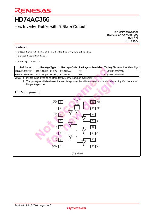
HD74AC366Hex Inverter Buffer with 3-State OutputREJ03D0270–0200Z(Previous ADE-205-391 (Z))Rev.2.00Jul.16.2004Features• 3-State Outputs Drive Bus Lines or Buffer Memory Address Registers • Outputs Source/Sink 24 mA • Ordering InformationPart Name Package Type Package Code Package Abbreviation Taping Abbreviation (Quantity)HD74AC366FPEL SOP-16 pin (JEITA)FP-16DAVFP EL (2,000 pcs/reel)HD74AC366RPELSOP-16 pin (JEDEC)FP-16DNVRPEL (2,500 pcs/reel)Notes: 1.Please consult the sales office for the above package availability.2.The packages with lead-free pins are distinguished from the conventional products by adding V at the end ofthe package code.Pin Arrangement12345678161514131211109OE 1V CC OE 2I I I O O OI I I GNDO O OLogic SymbolPin NamesOE 1, OE 23-State Output: Enable Input (Active Low)I Inputs OOutputsTruth TableInputs Output OE 1OE 2IOL L L H L L H L X H X Z H XXZH :High Voltage Level L :Low Voltage Level X :ImmaterialZ:High ImpedanceAbsolute Maximum RatingsItemSymbol RatingsUnit ConditionSupply voltage V CC –0.5 to 7V –20mA V I = –0.5V DC input diode current I IK 20mA V I = Vcc+0.5V DC input voltageV I –0.5 to Vcc+0.5V –50mA V O = –0.5V DC output diode current I OK 50mA V O = Vcc+0.5VDC output voltageV O –0.5 to Vcc+0.5V DC output source or sink currentI O±50mA DC V CC or ground current per output pin I CC , I GND ±50mA Storage temperatureTstg–65 to +150°CRecommended Operating ConditionsItemSymbol RatingsUnitConditionSupply voltageV CC 2 to 6V Input and Output voltage V I , V O 0 to V CC V Operating temperature Ta –40 to +85°C V CC = 3.0V V CC = 4.5 V Input rise and fall time (except Schmitt inputs)V IN 30% to 70% V CCtr, tf8ns/VV CC = 5.5 VDC CharacteristicsTa = 25°C Ta = –40 to +85°C ItemSym-bol Vcc (V)min.typ.max.min.max.UnitCondition3.0 2.1 1.5— 2.1—4.5 3.15 2.25— 3.15—V IH5.53.85 2.75— 3.85—V OUT = 0.1 V or V CC –0.1 V3.0— 1.500.9—0.94.5— 2.25 1.35— 1.35Input Voltage V IL5.5— 2.75 1.65— 1.65VV OUT = 0.1 V or V CC –0.1 V3.0 2.9 2.99— 2.9—4.5 4.4 4.49— 4.4—5.5 5.4 5.49— 5.4—V IN = V IL or V IH I OUT = –50 µA 3.0 2.58—— 2.48—I OH = –12 mA 4.53.94—— 3.80—I OH = –24 mA V OH5.5 4.94—— 4.80—V IN = V IL or V IHI OH = –24 mA3.0—0.0020.1—0.14.5—0.0010.1—0.15.5—0.0010.1—0.1V IN = V IL or V IH I OUT = 50 µA 3.0——0.32—0.37I OL = 12 mA 4.5——0.32—0.37I OL = 24 mA Output voltageV OL5.5——0.32—0.37VV IN = V IL or V IHI OL = 24 mAInput leakage current I IN 5.5——±0.1—±1.0µA V IN = V CC or GND 3 State currentI OZ5.5——±0.5—±5.0µA V IN(OE) = V IL , V IH V IN = V CC or GND V OUT = V CC or GND I OLD 5.5———86—mA V OLD = 1.1 V Dynamic output current *I OHD 5.5———–75—mA V OHD = 3.85 VQuiescent supply currentI CC5.5——8.0—80µAV IN = V CC or ground*Maximum test duration 2.0 ms, one output loaded at a time.AC CharacteristicsTa = +25°C C L = 50 pFTa = –40°C to +85°CC L = 50 pF ItemSymbol V CC (V)*1Min Typ Max Min Max UnitPropagation delay t PLH 3.3 1.07.09.0 1.010.0ns 5.0 1.0 5.07.0 1.07.5Propagation delay t PHL 3.3 1.07.09.0 1.010.0ns 5.0 1.0 4.57.0 1.07.5Enable time t ZH 3.3 1.09.013.0 1.013.5ns 5.0 1.07.09.5 1.010.0Enable time t ZL 3.3 1.010.012.5 1.013.5ns 5.0 1.07.59.5 1.010.0Disable time t HZ 3.3 1.09.512.0 1.012.5ns 5.0 1.07.510.0 1.010.5Disable time t LZ3.3 1.09.012.5 1.013.5ns5.01.07.010.01.010.5Note:1.Voltage Range 3.3 is 3.3 V ± 0.3 VVoltage Range 5.0 is 5.0 V ± 0.5 VCapacitanceItem Symbol Typ Unit ConditionInput capacitance CIN 4.5pF VCC= 5.5 VPower dissipation capacitance CPD 40.0pF VCC= 5.0 VPackage DimensionsPackage Code JEDECJEITAMass (reference value)FP-16DAV —Conforms 0.24 g*Ni/Pd/Au plating *0.40 ± 0.060.120.15M0.70 ± 0.20.1±1.271.27169181.75Max3.95*.2±.59.90˚– 8˚10.3 Max+ 0.10– 0.306.10+ 0.670.60+.11–.4.140.635 Max 1.08As of January, 2003 RENESAS SALES OFFICESRenesas Technology America, Inc.450 Holger Way, San Jose, CA 95134-1368, U.S.ATel: <1> (408) 382-7500 Fax: <1> (408) 382-7501Renesas Technology Europe Limited.Dukes Meadow, Millboard Road, Bourne End, Buckinghamshire, SL8 5FH, United KingdomTel: <44> (1628) 585 100, Fax: <44> (1628) 585 900Renesas Technology Europe GmbHDornacher Str. 3, D-85622 Feldkirchen, GermanyTel: <49> (89) 380 70 0, Fax: <49> (89) 929 30 11Renesas Technology Hong Kong Ltd.7/F., North Tower, World Finance Centre, Harbour City, Canton Road, Hong KongTel: <852> 2265-6688, Fax: <852> 2375-6836Renesas Technology Taiwan Co., Ltd.FL 10, #99, Fu-Hsing N. Rd., Taipei, TaiwanTel: <886> (2) 2715-2888, Fax: <886> (2) 2713-2999Renesas Technology (Shanghai) Co., Ltd.26/F., Ruijin Building, No.205 Maoming Road (S), Shanghai 200020, ChinaTel: <86> (21) 6472-1001, Fax: <86> (21) 6415-2952Renesas Technology Singapore Pte. Ltd.1, Harbour Front Avenue, #06-10, Keppel Bay Tower, Singapore 098632Tel: <65> 6213-0200, Fax: <65> 6278-8001© 2004. Renesas Technology Corp., All rights reserved. Printed in Japan.Colophon .1.0。

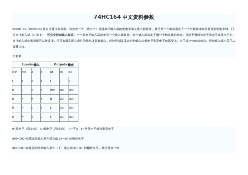
74HC164中文资料参数SN54HC164,/SN74HC164是8位移位寄存器,当其中一个(或二个)选通串行输入端的低电平禁止进入新数据,并把第一个触发器在下一个时钟脉冲来后复位到低电平时,门控串行输入端(A 和B)可完全控制输入数据。
一个高电平输入后就使另一个输入端赋能,这个输入就决定了第一个触发器的状态。
虽然不管时钟处于高电平或低电平时,串行输入端的数据都可以被改变,但只有满足建立条件的信息才能被输入。
时钟控制发生在时钟输入由低电平到高电平的跃变上。
为了减小传输线效应,所有输入端均采用二极管钳位。
功能表:H=高电平(稳定态) L=低电平(稳定态)×=不定↑=从低电平转换到高电平QA0…QH0=在稳定态输入条件建立前QA…QH 的相应电平QAn…QHn=在最近的时钟输入条件(↑)建立前QA…QH 的相应电平,表示移位一位图1 逻辑图(正逻辑)图2 引脚图Absolute Maximum Ratings绝对最大额定值Supply voltage range, 电源电压范围 VCC– V to 7V Input clamp current, 输入钳位电流 IIK (VI < 0 or VI > VCC) (see Note 1)±20 mA Output clamp current,输出钳位电流 IOK (VO < 0 or VO > VCC) (see Note 1)±20 mADC SPECIFICATIONS直流电气规格表:DC SPECIFICATIONS直流电气规格(续)电平电压 V---6 V---IOL = 4mA V---IOL= 6 V---II 输入漏VI = VCC or 0 6 V-±±100-±1000-±1000nA 电流ICC 静态电VI = VCC or 0,IO = 0 6 V--8-160-80μA 源电流Ci 电容-2V to 6V-310-10-10pF图3 参数测量信息图4 typical clear, shift, and clear sequence典型清除、移位和清除时序应用电路:图5 LCD驱动电路图6 LED驱动电路图7 4位数码显示电路。
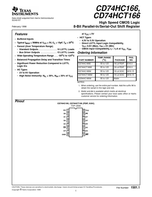
Data sheet acquired from Harris SemiconductorSCHS157Features•Buffered Inputs•Typical f MAX = 50MHz at V CC = 5V , C L = 15pF, T A = 25o C •Fanout (Over Temperature Range)-Standard Outputs. . . . . . . . . . . . . . .10 LSTTL Loads -Bus Driver Outputs . . . . . . . . . . . . .15 LSTTL Loads •Wide Operating Temperature Range . . .-55o C to 125o C •Balanced Propagation Delay and Transition Times •Significant Power Reduction Compared to LSTTL Logic ICs •HC Types-2V to 6V Operation-High Noise Immunity: N IL = 30%, N IH = 30% of V CCat V CC = 5V•HCT Types- 4.5V to 5.5V Operation-Direct LSTTL Input Logic Compatibility,V IL = 0.8V (Max), V IH = 2V (Min)-CMOS Input Compatibility, I l ≤1µA at V OL , V OHPinoutCD74HC166, CD74HCT166 (PDIP, SOIC)TOP VIEWOrdering InformationPART NUMBER TEMP . RANGE(o C)PACKAGE PKG.NO.CD74HC166E -55 to 12516 Ld PDIP E16.3CD74HCT166E -55 to 12516 Ld PDIP E16.3CD74HC166M -55 to 12516 Ld SOIC M16.15CD74HCT166M -55 to 12516 Ld SOIC M16.15CD54HC166W -55 to 125WaferNOTES:1.When ordering,use the entire part number.Add the suffix 96to obtain the variant in the tape and reel.2.Wafer and die is available which meets all electricalspecifications.Please contact your local sales office or Harris customer service for ordering information.14151691312111012345768DS D0D1D2D3CE GND CP V CC D7Q7D6D5D4MRPE February 1998CAUTION: These devices are sensitive to electrostatic discharge. Users should follow proper IC Handling Procedures.CD74HC166,CD74HCT166High Speed CMOS Logic8-Bit Parallel-In/Serial-Out Shift RegisterFile Number1501.1[ /Title (CD74HC166,CD74HCT166)/Sub-ject (High Speed CMOS Logic 8-Bit Paral-lel-In/Seri元器件交易网Functional DiagramTRUTH TABLEINPUTSINTERNAL Q STATESOUTPUT Q7MASTER RESETPARALLEL ENABLECLOCK ENABLECLOCK SERIAL PARALLELD0 D7Q0Q1L X X X X X L L L H X L L X X Q00Q10Q0H L L ↑X a...h a b h H H L ↑H X H Q0n Q6n H H L ↑L X L Q0n Q6n HXH↑XXQ00Q10Q70NOTES:H = High Voltage Level L = Low Voltage Level X = Don’t Care↑= T ransition from Low to High Levela...h = The level of steady-state input at inputs D0 thru D7, respectively.Q00, Q10, Q70= The level of Q0, Q1, or Q7, respectively, before the indicated steady-state input conditions were established.Q0n, Q6n =The level of Q0 or Q6, respectively , before the most recent ↑ transition of the clock.8 - REGISTERSP ARALLEL ENABLE CIRCUIT D0D1D2D3D4D5D6D7PED SCP CE MRD0D7Q7Absolute Maximum Ratings Thermal InformationDC Supply Voltage, V CC. . . . . . . . . . . . . . . . . . . . . . . .-0.5V to 7V DC Input Diode Current, I IKFor V I < -0.5V or V I > V CC + 0.5V. . . . . . . . . . . . . . . . . . . . . .±20mA DC Output Diode Current, I OKFor V O < -0.5V or V O > V CC + 0.5V . . . . . . . . . . . . . . . . . . . .±20mA DC Drain Current, per Output, I OFor -0.5V < V O < V CC + 0.5V. . . . . . . . . . . . . . . . . . . . . . . . . .±25mA DC Output Source or Sink Current per Output Pin, I OFor V O > -0.5V or V O < V CC + 0.5V . . . . . . . . . . . . . . . . . . . .±25mA DC V CC or Ground Current, I CC or I GND. . . . . . . . . . . . . . . . . .±50mA Operating ConditionsTemperature Range (T A) . . . . . . . . . . . . . . . . . . . . .-55o C to 125o C Supply Voltage Range, V CCHC T ypes . . . . . . . . . . . . . . . . . . . . . . . . . . . . . . . . . . . . .2V to 6V HCT T ypes . . . . . . . . . . . . . . . . . . . . . . . . . . . . . . . . .4.5V to 5.5V DC Input or Output Voltage, V I, V O . . . . . . . . . . . . . . . . .0V to V CC Input Rise and Fall Time2V . . . . . . . . . . . . . . . . . . . . . . . . . . . . . . . . . . . . . .1000ns (Max) 4.5V. . . . . . . . . . . . . . . . . . . . . . . . . . . . . . . . . . . . . .500ns (Max) 6V . . . . . . . . . . . . . . . . . . . . . . . . . . . . . . . . . . . . . . .400ns (Max)Thermal Resistance (T ypical, Note 3)θJA (o C/W) PDIP Package. . . . . . . . . . . . . . . . . . . . . . . . . . . . .90 SOIC Package. . . . . . . . . . . . . . . . . . . . . . . . . . . . .160 Maximum Junction T emperature. . . . . . . . . . . . . . . . . . . . . . .150o C Maximum Storage Temperature Range . . . . . . . . . .-65o C to 150o C Maximum Lead Temperature (Soldering 10s). . . . . . . . . . . . .300o C (SOIC - Lead Tips Only)CAUTION:Stresses above those listed in“Absolute Maximum Ratings”may cause permanent damage to the device.This is a stress only rating and operation of the device at these or any other conditions above those indicated in the operational sections of this specification is not implied.NOTE:3.θJA is measured with the component mounted on an evaluation PC board in free air.DC Electrical SpecificationsPARAMETER SYMBOLTESTCONDITIONSV CC (V)25o C-40o C TO 85o C-55o C TO 125o CUNITS V I(V)I O(mA)MIN TYP MAX MIN MAX MIN MAXHC TYPESHigh Level Input Voltage V IH--2 1.5-- 1.5- 1.5-V4.5 3.15-- 3.15 - 3.15-V6 4.2-- 4.2- 4.2-VLow Level Input Voltage V IL--2--0.5-0.5-0.5V4.5-- 1.35- 1.35- 1.35V6-- 1.8- 1.8- 1.8VHigh Level Output VoltageCMOS Loads V OH V IH orV IL-0.022 1.9-- 1.9- 1.9-V-0.02 4.5 4.4-- 4.4 - 4.4-V-0.026 5.9-- 5.9- 5.9-VHigh Level Output VoltageTTL Loads-4 4.5 3.98-- 3.84- 3.7-V -5.26 5.48-- 5.34- 5.2-VLow Level Output VoltageCMOS Loads V OL V IH orV IL0.022--0.1-0.1-0.1V0.02 4.5--0.1-0.1-0.1V0.026--0.1-0.1-0.1VLow Level Output VoltageTTL Loads4 4.5--0.26-0.33-0.4V5.26--0.26-0.33-0.4VInput Leakage Current I I V CC orGND-6--±0.1-±1-±1µAQuiescent Device Current I CCV CC or GND6--8-80-160µAHCT TYPES High Level Input Voltage V IH -- 4.5 to 5.52--2-2-V Low Level Input VoltageV IL -- 4.5 to 5.5--0.8-0.8-0.8V High Level Output VoltageCMOS Loads V OHV IH or V IL-0.024.54.4-- 4.4- 4.4-VHigh Level Output Voltage TTL Loads -4 4.5 3.98-- 3.84- 3.7-VLow Level Output VoltageCMOS Loads V OLV IH or V IL0.02 4.5--0.1-0.1-0.1VLow Level Output Voltage TTL Loads 4 4.5--0.26-0.33-0.4VInput Leakage CurrentI I V CC to GND 0 5.5--±0.1-±1-±1µA Quiescent Device CurrentI CC V CC or GND 0 5.5--8-80-160µA Additional Quiescent Device Current Per Input Pin: 1 Unit Load (Note 4)∆I CCV CC -2.1-4.5 to5.5-100360-450-490µANOTE:4.For dual-supply systems theoretical worst case (V I = 2.4V, V CC =5.5V) specification is 1.8mA.DC Electrical Specifications(Continued)PARAMETER SYMBOL TEST CONDITIONSV CC (V)25o C -40o C TO 85o C -55o C TO 125o C UNITS V I (V)I O (mA)MIN TYP MAX MIN MAX MIN MAX HCT Input Loading TableINPUT UNIT LOADSDS, D0-D70.2PE 0.35CP,CE 0.5MR0.2NOTE:Unit Load is ∆I CC limit specified in DC Electrical Specifications table, e.g., 360µA max at 25o C.Prerequisite For Switching SpecificationsPARAMETERSYMBOLV CC (V)25o C-40o C TO 85o C -55o C TO 125o C UNITSMINMAXMINMAXMINMAXHC TYPES Clock Frequency (Figure 1)f MAX26-5-4-MHz 4.530-25-20-MHz 635-29-23-MHzMR Pulse Width (Figure 1)t w2100-125-150-ns4.520-25-30-ns617-21-26-nsClock Pulse Width (Figure 1)t W280-100-120-ns4.516-20-24-ns614-17-20-nsSet-up TimeData and CE to Clock (Figure 5)t SU280-100-120-ns4.516-20-24-ns614-17-20-nsHold Time Data to Clock (Figure 5)t H21-1-1-ns4.51-1-1-ns61-1-1-nsRemoval Time MR to Clock (Figure 5)t REM20-0-0-ns4.50-0-0-ns60-0-0-nsSet-up Time PE to CP (Figure 5)t SU2145-180-220-ns4.529-36-44-ns625-31-38-nsHold TimePE to CP or CE (Figure 5)t H20-0-0-ns4.50-0-0-ns60-0-0-nsHCT TYPESClock Frequency (Figure 2)f MAX 4.525-20-16-MHz MR Pulse Width (Figure 2)t w 4.535-44-53-ns Clock Pulse Width (Figure 2)t w 4.520-25-30-ns Set-up Time Data and CE toClock (Figure 6)t SU 4.516-20-24-nsHold Time Data to Clock(Figure 6)t H 4.50-0-0-nsRemoval Time MR to Clock(Figure 6)t REM 4.50-0-0-ns Set-up Time PE to CP(Figure6)t SU 4.530-38-45-nsHold Time PE to CP or CE(Figure 6)t H 4.50-0-0-ns Switching Specifications Input t r, t f = 6nsPARAMETER SYMBOLTESTCONDITIONS V CC (V)25o C-40o C TO 85o C-55o C TO125o CUNITSTYP MAX MAX MAXHC TYPESPropagation Delay, Clock to Output (Figure 3)t PLH, t PHL C L= 50pF2-160200240ns4.5-324048nsC L= 15pF513---nsCL = 50pF6-273441nsPrerequisite For Switching Specifications (Continued)PARAMETER SYMBOL V CC (V)25o C-40o C TO 85o C-55o C TO 125o CUNITS MIN MAX MIN MAX MIN MAXOutput Transition Time (Figure 3)t TLH , t THLC L = 50pF2-7595110ns 4.5-151922ns 6-131619ns Propagation Delay MR to Output (Figure 3)t PHLC L = 50pF2-160200240ns 4.5-324048ns 6-273441ns Input Capacitance C I ---101010pF Power Dissipation Capacitance (Notes 5, 6)C PD-541---pFHCT TYPESPropagation Delay,Clock to Output (Figure 4)t PLH , t PHL C L = 50pF4.5-405060nsOutput Transition Time (Figure 4)t TLH , t THL C L = 50pF 4.5-151922ns Propagation DelayMR to Output (Figure 4)t PHL C L = 50pF4.5-405060ns Input Capacitance C I---101010pFNOTES:5.C PD is used to determine the dynamic power consumption, per gate.6.P D =C PD V CC 2f i +∑(C L V CC 2+f O )where f i =Input Frequency,f O =Output Frequency,C L =Output Load Capacitance,V CC =Supply Voltage.Switching SpecificationsInput t r , t f = 6ns (Continued)PARAMETERSYMBOL TEST CONDITIONS V CC (V)25o C-40o C TO 85o C -55o C TO 125o CUNITS TYP MAX MAX MAX Test Circuits and WaveformsNOTE:Outputs should be switching from 10% V CC to 90% V CC in accordance with device truth table.For f MAX ,input duty cycle =50%.FIGURE 1.HC CLOCK PULSE RISE AND FALL TIMES ANDPULSE WIDTHNOTE:Outputs should be switching from 10% V CC to 90% V CC in accordance with device truth table.For f MAX ,input duty cycle =50%.FIGURE 2.HCT CLOCK PULSE RISE AND FALL TIMES ANDPULSE WIDTHCLOCK90%50%10%GNDV CCt r C L t f C L 50%50%t WLt WH10%t WL + t WH =f CLI CLOCK 2.7V 1.3V0.3VGND3Vt r C L = 6nst f C L = 6ns1.3V 1.3V t WLt WH0.3V t WL + t WH =fC L IFIGURE 3.HC AND HCU TRANSITION TIMES AND PROPAGA-TION DELAY TIMES, COMBINATION LOGIC FIGURE 4.HCT TRANSITION TIMES AND PROPAGATIONDELAY TIMES, COMBINATION LOGICFIGURE 5.HC SETUP TIMES,HOLD TIMES,REMOVAL TIME,AND PROPAGATION DELAY TIMES FOR EDGE TRIGGERED SEQUENTIAL LOGIC CIRCUITS FIGURE 6.HCT SETUP TIMES,HOLD TIMES,REMOVAL TIME,AND PROPAGATION DELAY TIMES FOR EDGE TRIGGERED SEQUENTIAL LOGIC CIRCUITSTest Circuits and Waveforms (Continued)t PHLt PLHt THLt TLH 90%50%10%50%10%INVERTING OUTPUTINPUTGNDV CCt r = 6nst f = 6ns90%t PHLt PLHt THLt TLH 2.7V 1.3V 0.3V1.3V 10%INVERTING OUTPUTINPUTGND3Vt r = 6nst f = 6ns90%t r C Lt f C LGNDV CC GNDV CC50%90%10%GNDCLOCK INPUTDATA INPUT OUTPUTSET, RESET OR PRESETV CC50%50%90%10%50%90%t REMt PLHt SU(H)t TLH t THL t H(L)t PHLICC L 50pF t SU(L)t H(H)t r C Lt f C LGND3VGND3V1.3V2.7V 0.3VGNDCLOCK INPUTDATA INPUT OUTPUTSET, RESET OR PRESET3V1.3V1.3V 1.3V90%10%1.3V 90%t REMt PLHt SU(H)t TLHt THLt H(L)t PHLICC L 50pFt SU(L)1.3Vt H(H)1.3VIMPORTANT NOTICETexas Instruments and its subsidiaries (TI) reserve the right to make changes to their products or to discontinue any product or service without notice, and advise customers to obtain the latest version of relevant information to verify, before placing orders, that information being relied on is current and complete. All products are sold subject to the terms and conditions of sale supplied at the time of order acknowledgement, including those pertaining to warranty, patent infringement, and limitation of liability.TI warrants performance of its semiconductor products to the specifications applicable at the time of sale in accordance with TI’s standard warranty. Testing and other quality control techniques are utilized to the extent TI deems necessary to support this warranty. Specific testing of all parameters of each device is not necessarily performed, except those mandated by government requirements.CERTAIN APPLICATIONS USING SEMICONDUCTOR PRODUCTS MAY INVOLVE POTENTIAL RISKS OF DEATH, PERSONAL INJURY, OR SEVERE PROPERTY OR ENVIRONMENTAL DAMAGE (“CRITICAL APPLICATIONS”). TI SEMICONDUCTOR PRODUCTS ARE NOT DESIGNED, AUTHORIZED, OR WARRANTED TO BE SUITABLE FOR USE IN LIFE-SUPPORT DEVICES OR SYSTEMS OR OTHER CRITICAL APPLICATIONS. INCLUSION OF TI PRODUCTS IN SUCH APPLICATIONS IS UNDERSTOOD TO BE FULLY AT THE CUSTOMER’S RISK.In order to minimize risks associated with the customer’s applications, adequate design and operating safeguards must be provided by the customer to minimize inherent or procedural hazards.TI assumes no liability for applications assistance or customer product design. TI does not warrant or represent that any license, either express or implied, is granted under any patent right, copyright, mask work right, or other intellectual property right of TI covering or relating to any combination, machine, or process in which such semiconductor products or services might be or are used. TI’s publication of information regarding any third party’s products or services does not constitute TI’s approval, warranty or endorsement thereof.Copyright © 1998, Texas Instruments Incorporated。
元器件交易网IMPORTANT NOTICETexas Instruments and its subsidiaries (TI) reserve the right to make changes to their products or to discontinueany product or service without notice, and advise customers to obtain the latest version of relevant informationto verify, before placing orders, that information being relied on is current and complete. All products are soldsubject to the terms and conditions of sale supplied at the time of order acknowledgement, including thosepertaining to warranty, patent infringement, and limitation of liability.TI warrants performance of its semiconductor products to the specifications applicable at the time of sale inaccordance with TI’s standard warranty. Testing and other quality control techniques are utilized to the extentTI deems necessary to support this warranty. Specific testing of all parameters of each device is not necessarilyperformed, except those mandated by government requirements.CERTAIN APPLICATIONS USING SEMICONDUCTOR PRODUCTS MAY INVOLVE POTENTIAL RISKS OFDEATH, PERSONAL INJURY, OR SEVERE PROPERTY OR ENVIRONMENTAL DAMAGE (“CRITICALAPPLICATIONS”). TI SEMICONDUCTOR PRODUCTS ARE NOT DESIGNED, AUTHORIZED, ORWARRANTED TO BE SUITABLE FOR USE IN LIFE-SUPPORT DEVICES OR SYSTEMS OR OTHERCRITICAL APPLICATIONS. INCLUSION OF TI PRODUCTS IN SUCH APPLICATIONS IS UNDERSTOOD TOBE FULLY AT THE CUSTOMER’S RISK.In order to minimize risks associated with the customer’s applications, adequate design and operatingsafeguards must be provided by the customer to minimize inherent or procedural hazards.TI assumes no liability for applications assistance or customer product design. TI does not warrant or representthat any license, either express or implied, is granted under any patent right, copyright, mask work right, or otherintellectual property right of TI covering or relating to any combination, machine, or process in which suchsemiconductor products or services might be or are used. TI’s publication of information regarding any thirdparty’s products or services does not constitute TI’s approval, warranty or endorsement thereof.Copyright © 1998, Texas Instruments Incorporated。
HD74HCT1G66Analog SwitchREJ03D0197–0700Z(Previous ADE-205-308E (Z))Rev.7.00Jan.29.2004 DescriptionThe HD74HCT1G66 is high-speed CMOS analog switch using silicon gate CMOS process. With CMOS low power dissipation, it provides high speed. The device has low ON resistance for good transfer characteristics and can take wide range of input voltage.Features•The basic gate function is lined up as Renesas uni logic series.•Supplied on emboss taping for high-speed automatic mounting.•Control input is TTL compatible input level.Supply voltage range : 4.5 to 5.5 VOperating temperature range : –40 to +85°C•|I OH| = I OL = 2 mA (min)•Ordering InformationPart Name Package Type Package Code PackageAbbreviation Taping Abbreviation (Quantity)HD74HCT1G66CME CMPAK-5 pin CMPAK-5V CM E (3,000 pcs/reel)Outline and Article IndicationFunction TableControl Switch L OFFH ONH : High levelL : Low levelGND ≤ V IN≤ V CCGND ≤ V OUT≤ V CCPin ArrangementAbsolute Maximum RatingsItem Symbol Ratings Unit Test Conditions Supply voltage range V CC–0.5 to 7.0VInput voltage range *1V I–0.5 to V CC + 0.5VOutput voltage range *1, 2V O–0.5 to V CC + 0.5V Output : H or LInput clamp current I IK±20mA V I < 0 or V I > V CC Output clamp current I OK±20mA V O < 0 or V O >V CC Continuous output current I O±25mA V O = 0 to V CC Continuous current throughI CC or I GND±25mAV CC or GNDP T200mWMaximum power dissipationat Ta = 25°C (in still air) *3Storage temperature Tstg–65 to 150°CNotes:The absolute maximum ratings are values, which must not individually be exceeded, and furthermore, no two of which may be realized at the same time.1.The input and output voltage ratings may be exceeded if the input and output clamp-currentratings are observed.2.This value is limited to 5.5 V maximum.3.The maximum package power dissipation was calculated using a junction temperature of 150°C. Recommended Operating ConditionsItem Symbol Min Max Unit Test Conditions Supply voltage range V CC 4.5 5.5VInput voltage range V I0 5.5VOutput voltage range V I/O0V CC Vt r, t f0500ns V CC = 4.5 to 5.5 V Input rise / fall time(Control input 0.3 V to 2.7 V)Operating temperature Ta–4085°CNote:Unused or floating control inputs must be held high or low.Electrical CharacteristicsTa = 25°C Ta = –40 to 85°CItem Symbl V CC(V)Min Typ Max Min Max Unit Test Conditions V IH 4.5 to 5.5 2.0—— 2.0—Input voltageV IL4.5 to5.5——0.8—0.8VControl input onlyOn resistanceR ON4.5 to5.5—90160—180ΩV C = V IHV IN = V CC or GND I T = 1 mA Peak on resistance R ON (p) 4.5 to 5.5—125200—250ΩV C = V IHV IN = 0 to V CC I IN/OUT = 1 mA I S (off) 5.5——±0.1—±1.0µAV C = V ILV IN = V CC , V OUT = GND or V IN = GND,V OUT = V CCLeak currentI S (on)5.5——±0.1—±1.0µA V C = V IHV IN = V CC or GND Input current I IN 5.5——±0.1—±1.0µA V IN = V CC or GND Operating current I CC 5.5—— 1.0—10.0µA V IN = V CC or GND Quiescent supply currentI CCT5.5——2.0—2.9mAV C = 2.4 V,V IN (switch) = V CC or GNDSwitching CharacteristicsTa = 25°C Ta = –40 to 85°CItemSymbl V CC(V)Min Typ Max Min Max Unit TestConditions Propagation delay time t PLH ,t PHL 4.5—410—13ns R L = 10 k ΩOutput enable time t ZH , t ZL 4.5—1023—29ns R L = 1 k ΩOutput disable time t HZ , t LZ4.5—1423—29ns R L = 1 k ΩMaximum control frequency 4.5—30———MHz Control input capacitanceC IN — 2.55—5pF Switch I/O capacitance C IN/OUT — 2.5———pF Feed through capacitance C IN–OUT —0.5———pF Power dissipation capacitanceC PD —5———pFTest CircuitPackage Dimensions RENESAS SALES OFFICESRenesas Technology America, Inc.450 Holger Way, San Jose, CA 95134-1368, U.S.ATel: <1> (408) 382-7500 Fax: <1> (408) 382-7501Renesas Technology Europe Limited.Dukes Meadow, Millboard Road, Bourne End, Buckinghamshire, SL8 5FH, United KingdomTel: <44> (1628) 585 100, Fax: <44> (1628) 585 900Renesas Technology Europe GmbHDornacher Str. 3, D-85622 Feldkirchen, GermanyTel: <49> (89) 380 70 0, Fax: <49> (89) 929 30 11Renesas Technology Hong Kong Ltd.7/F., North Tower, World Finance Centre, Harbour City, Canton Road, Hong KongTel: <852> 2265-6688, Fax: <852> 2375-6836Renesas Technology Taiwan Co., Ltd.FL 10, #99, Fu-Hsing N. Rd., Taipei, TaiwanTel: <886> (2) 2715-2888, Fax: <886> (2) 2713-2999Renesas Technology (Shanghai) Co., Ltd.26/F., Ruijin Building, No.205 Maoming Road (S), Shanghai 200020, ChinaTel: <86> (21) 6472-1001, Fax: <86> (21) 6415-2952Renesas Technology Singapore Pte. Ltd.1, Harbour Front Avenue, #06-10, Keppel Bay Tower, Singapore 098632Tel: <65> 6213-0200, Fax: <65> 6278-8001。
7400 QUAD 2-INPUT NAND GATES与非门7401 QUAD 2-INPUT NAND GATES OC与非门7402 QUAD 2-INPUT NOR GA TES或非门7403 QUAD 2-INPUT NAND GATES与非门7404 HEX INVERTING GA TES反向器7406 HEX INVERTING GA TES HV高输出反向器7408 QUAD 2-INPUT AND GA TE与门7409 QUAD 2-INPUT AND GA TES OC与门7410 TRIPLE 3-INPUT NAND GATES与非门7411 TRIPLE 3-INPUT AND GA TES与门74121 ONE-SHOT WITH CLEAR单稳态74132 SCHMITT TRIGGER NAND GATES 触发器与非门7414 SCHMITT TRIGGER INVERTERS触发器反向器74153 4-LINE TO 1 LINE SELECTOR四选一74155 2-LINE TO 4-LINE DECODER译码器74180 PARITY GENERATOR/CHECKER奇偶发生检验74191 4-BIT BINARY COUNTER UP/DOWN计数器7420 DUAL 4-INPUT NAND GA TES双四输入与非门7426 QUAD 2-INPUT NAND GATES与非门7427 TRIPLE 3-INPUT NOR GA TES三输入或非门7430 8-INPUT NAND GATES八输入端与非门7432 QUAD 2-INPUT OR GA TES二输入或门7438 2-INPUT NAND GATE BUFFER与非门缓冲器7445 BCD-DECIMAL DECODER/DRIVER BCD译码驱动器7474 D-TYPE FLIP-FLOP D型触发器7475 QUAD LATCHES双锁存器7476 J-K FLIP-FLOP J-K触发器7485 4-BIT MAGNITUDE COMPARATOR四位比较器7486 2-INPUT EXCLUSIVE OR GATES双端异或门74HC00 QUAD 2-INPUT NAND GATES双输入与非门74HC02 QUAD 2-INPUT NOR GATES双输入或非门74HC03 2-INPUT OPEN-DRAIN NAND GATES与非门74HC04 HEX INVERTERS六路反向器74HC05 HEX INVERTERS OPEN DRAIN六路反向器74HC08 2-INPUT AND GA TES双输入与门74HC107 J-K FLIP-FLOP WITH CLEAR J-K触发器74HC109A J-K FLIP-FLOP W/PRESET J-K触发器74HC11 TRIPLE 3-INPUT AND GATES三输入与门74HC112 DUAL J-K FLIP-FLOP双J-K触发器74HC113 DUAL J-K FLIP-FLOP PRESET双JK触发器74HC123A RETRIGGERABLE MONOSTAB可重触发单稳74HC125 TRI-STATE QUAD BUFFERS四个三态门74HC126 TRI-STATE QUAD BUFFERS六三态门74HC132 2-INPUT TRIGGER NAND 施密特触发与非门74HC133 13-INPUT NAND GATES十三输入与非门74HC137 3-TO-8 DECODERS W/LATCHES 3-8线译码器74HC138 3-8 LINE DECODER3线至8线译码器74HC139 2-4 LINE DECODER2线至4线译码器74HC14 TRIGGERED HEX INVERTER六触发反向器74HC147 10-4 LINE PRIORITY ENCODER 10-4编码器74HC148 8-3 LINE PRIORITY ENCODER8-3编码器74HC149 8-8 LINE PRIORITY ENCODER 8-8编码器74HC151 8-CHANNEL DIGITAL MUX8通道多路器74HC153 DUAL 4-INPUT MUX双四输入多路器74HC154 4-16 LINE DECODER4线至16线译码器74HC155 2-4 LINE DECODER2线至4线译码器74HC157 QUAD 2-INPUT MUX四个双端多路器74HC161 BINARY COUNTER二进制计数器74HC163 DECADE COUNTERS十进制计数器74HC164 SERIAL-PARALLEL SHIFT REG串入并出74HC165 PARALLEL-SERIAL SHIFT REG并入串出74HC166 SERIAL-PARALLEL SHIFT REG串入并出74HC173 TRI-STATE D FLIP-FLOP三态D触发器74HC174 HEX D FLIP-FLOP W/CLEAR六D触发器74HC175 HEX D FLIP-FLOP W/CLEAR六D触发器74HC181 ARITHMETIC LOGIC UNIT算术逻辑单元74HC182 LOOK AHEAD CARRYGENERATR进位发生器74HC190 BINARY UP/DN COUNTER 二进制加减计数器74HC191 DECADE UP/DN COUNTER 十进制加减计数器74HC192 DECADE UP/DN COUNTER 十进制加减计数器74HC193 BINARY UP/DN COUNTER 二进制加减计数器74HC194 4BIT BI-DIR SHIFT4位双向移位寄存器74HC195 4BIT PARALLEL SHIFT 4位并行移位寄存器74HC20 QUAD 4-INPUT NAND GATE四个四入与非门74HC221A NON-RETRIG MONOSTAB不可重触发单稳74HC237 3-8 LINE DECODER 地址锁3线至8线译码器74HC242/243 TRI-STAT TRANSCEIVER三态收发器74HC244 OCTAL 3-STATE BUFFER八个三态缓冲门74HC245 OCTAL 3-STATE TRANSCEIVER三态收发器74HC251 8-CH 3-STA TE MUX8路3态多路器74HC253 DUAL 4-CH 3-STATE MUX4路3态多路器74HC257 QUAD 2-CH 3-STATE MUX4路3态多路器74HC258 2-CH 3-STA TE MUX2路3态多路器74HC259 3-8 LINE DECODER8位地址锁存译码器74HC266A 2-INPUT EXCLUSIVE NOR GA TE异或非74HC27 TRIPLE 3-INPUT NOR GATE三个3输入或非门74HC273 OCTAL D FLIP-FLOP CLEAR8路D触发器74HC280 9BIT ODD/EVEN GENERATOR奇偶发生器74HC283 4BIT BINARY ADDER CARRY四位加法器74HC299 3-STATE UNIVERSAL SHIFT三态移位寄存74HC30 8-INPUT NAND GATE8输入端与非门74HC32 QUAD 2-INPUT OR GA TE四个双端或门74HC34 NON-INVERTER非反向器74HC354 8-CH 3-STA TE MUX8路3态多路器74HC356 8-CH 3-STA TE MUX8路3态多路器74HC365 HEX 3-STATE BUFFER六个三态缓冲门74HC366 3-STATE BUFFER INVERTER缓冲反向器74HC367 3-STATE BUFFER INVERTER缓冲反向器74HC368 3-STATE BUFFER INVERTER缓冲反向器74HC373 3-STATE OCTAL D LATCHES 三态D型锁存器74HC374 3-STATE OCTAL D FLIPFLOP三态D触发器74HC3934-BIT BINARY COUNTER 4位二进制计数器74HC4016 QUAD ANALOG SWITCH四路模拟量开关74HC4020 14-Stage Binary Counter 14输出计数器74HC4017 Decade Counter/Divider with 10 Decoded Outputs 十进制计数器带10个译码输出端74HC4040 12 Stage Binary Counter12出计数器74HC4046 PHASE LOCK LOOP相位监测输出器74HC4049 LEVEL DOWN CONVERTER电平变低器74HC4050 LEVEL DOWN CONVERTER电平变低器74HC4051 8-CH ANALOG MUX8通道多路器74HC4052 4-CH ANALOG MUX4通道多路器74HC4053 2-CH ANALOG MUX2通道多路器74HC4060 14-STAGE BINARY COUNTER14阶BIN计数74HC4066 QUAD ANALOG MUX四通道多路器74HC4075 TRIPLE 3-INPUT OR GATE3输入或门74HC42 BCD TO DECIMAL BCD转十进制译码器74HC423A RETRIGGERABLE MONOSTAB可重触发单稳74HC4511 BCD-7 SEG DRIVER/DECODER7段译码器74HC4514 4-16 LINE DECODER4至16线译码器74HC4538A RETRIGGERAB MONOSTAB可重触发单稳74HC4543 LCD BCD-7 SEG LCD用的BCD-7段译码驱动74HC51 AND OR GATE INVERTER与或非门74HC521 8BIT MAGNITUDE COMPARA TOR判决定路74HC533 3-STATE D LATCH三态D锁存器74HC534 3-STATE D FLIP-FLOP三态D型触发器74HC540 3-STATE BUFFER三态缓冲器74HC541 3-STATE BUFFER INVERTER三态缓冲反向器74HC58 DUAL AND OR GATE与或门74HC589 3STATE 8BIT SHIFT 8位移位寄存三态输出74HC594 8BIT SHIFT REG8位移位寄存器74HC595 8BIT SHIFT REG8位移位寄存器出锁存74HC597 8BIT SHIFT REG8位移位寄存器入锁存74HC620 3-STATE TRANSCEIVER反向3态收发器74HC623 3-STATE TRANSCEIVER八路三态收发器74HC640 3-STATE TRANSCEIVER反向3态收发器74HC643 3-STATE TRANSCEIVER八路三态收发器74HC646 NON-INVERT BUS TRANSCEIVER 总线收发器74HC648 INVERT BUS TRANCIVER反向总线收发器74HC688 8BIT MAGNITUDE COMPARA TOR 8位判决电路74HC7266 2-INPUT EXCLUSIVE NOR GA TE异或非门74HC73 DUAL J-K FLIP-FLOP W/CLEAR双JK触发器74HC74A PRESET/CLEAR D FLIP-FLOP双D触发器74HC75 4BIT BISTABLE LATCH4位双稳锁存器74HC76 PRESET/CLEAR JK FLIP-FLOP双JK触发器74HC85 4BIT MAGNITUDE COMPARATOR4位判决电路74HC86 2INPUT EXCLUSIVE OR GATE2输入异或门74HC942 BAUD MODEM300BPS低速调制解调器74HC943 300 BAUD MODEM300BPS低速调制解调器74LS00 QUAD 2-INPUT NAND GATES与非门74LS02 QUAD 2-INPUT NOR GATES或非门74LS03 QUAD 2-INPUT NAND GATES与非门74LS04 HEX INVERTING GA TES反向器74LS05 HEX INVERTERS OPEN DRAIN六路反向器74LS08 QUAD 2-INPUT AND GA TE与门74LS09 QUAD 2-INPUT AND GA TES OC与门74LS10 TRIPLE 3-INPUT NAND GATES与非门74LS109 QUAD 2-INPUT AND GATES OC与门74LS11 TRIPLE 3-INPUT AND GA TES与门74LS112 DUAL J-K FLIP-FLOP双J-K触发器74LS113 DUAL J-K FLIP-FLOP PRESET双JK触发器74LS114 NEGATIVE J-K FLIP-FLOP负沿J-K触发器74LS122 Retriggerable Monostab可重触发单稳74LS123 Retriggerable Monostable 可重触发单稳74LS125 TRI-STATE QUAD BUFFERS四个三态门74LS13 QUAL 4-in NAND TRIGGER 4输入与非触发器74LS160 BCD DECADE 4BIT BIN COUNTERS计数器74LS136 QUADRUPLE 2-INPUT XOR GATE异或门74LS138 3-8 LINE DECODER3线至8线译码器74LS139 2-4 LINE DECODER2线至4线译码器74LS14 TRIGGERED HEX INVERTER六触发反向器74HC147 10-4 LINE PRIORITY ENCODER 10-4编码器74HC148 8-3 LINE PRIORITY ENCODER 8-3编码器74HC149 8-8 LINE PRIORITY ENCODER 8-8编码器74LS151 8-CHANNEL DIGITAL MUX8通道多路器74LS153 DUAL 4-INPUT MUX双四输入多路器74LS155 2-4 LINE DECODER2线至4线译码器74LS156 2-4 LINE DECODER/DEMUX2-4译码器74LS157 QUAD 2-INPUT MUX四个双端多路器74LS158 2-1 LINE MUX2-1线多路器74LS160A BINARY COUNTER二进制计数器74LS161A BINARY COUNTER二进制计数器74LS162A BINARY COUNTER二进制计数器74LS163A DECADE COUNTERS十进制计数器74LS164 SERIAL-PARALLEL SHIFT REG串入并出74LS168 BI-DIRECT BCD TO DECADE双向计数器74LS169 4BIT UP/DN BIN COUNTER 四位加减计数器74LS173 TRI-STATE D FLIP-FLOP三态D触发器74LS174 HEX D FLIP-FLOP W/CLEAR六D触发器74LS175 HEX D FLIP-FLOP W/CLEAR六D触发器74LS190 BINARY UP/DN COUNTER 二进制加减计数器74LS191 DECADE UP/DN COUNTER 十进制加减计数器74LS192 DECADE UP/DN COUNTER 十进制加减计数器74LS193 BINARY UP/DN COUNTER 二进制加减计数器74LS194A 4BIT BI-DIR SHIFT4位双向移位寄存器74LS195A 4BIT PARALLEL SHIFT4位并行移位寄存器74LS20 QUAD 4-INPUT NAND GATE四个四入与非门74LS21 4-INPUT AND GA TE四输入端与门74LS240 OCTAL 3-STATE BUFFER八个三态缓冲门74LS244 OCTAL 3-STATE BUFFER八个三态缓冲门74LS245 OCTAL 3-STATE TRANSCEIVER三态收发器74LS253 DUAL 4-CH 3-STATE MUX4路3态多路器74LS256 4BIT ADDRESS LATCH四位可锁存锁存器74LS257 QUAD 2-CH 3-STATE MUX4路3态多路器74LS258 2-CH 3-STA TE MUX2路3态多路器74LS27 TRIPLE 3-INPUT NOR GATES三输入或非门74LS279 QUAD R-S LATCHES四个RS非锁存器74LS28 QUAD 2-INPUT NOR BUFFER 四双端或非缓冲74LS283 4BIT BINARY ADDER CARRY四位加法器74LS30 8-INPUT NAND GATES八输入端与非门74LS32 QUAD 2-INPUT OR GA TES二输入或门74LS352 4-1 LINE SELECTOR/MUX 4-1线选择多路器74LS365 HEX 3-STA TE BUFFER六个三态缓冲门74LS367 3-STATE BUFFER INVERTER缓冲反向器74LS368A 3-STATE BUFFER INVERTER缓冲反向器74LS373 OCT LATCH W/3-STA TE OUT三态输出锁存器74LS76 Dual JK Flip-Flop w/set2个JK触发器74LS379 QUAD PARALLEL REG四个并行寄存器74LS38 2-INPUT NAND GATE BUFFER与非门缓冲器74LS390 DUAL DECADE COUNTER2个10进制计数器74LS393 DUAL BINARY COUNTER2个2进制计数器74LS42 BCD TO DECIMAL BCD转十进制译码器74LS48 BCD-7 SEG BCD-7段译码器74LS49 BCD-7 SEG BCD-7段译码器74LS51 AND OR GATE INVERTER与或非门74LS540 OCT Buffer/Line Driver8路缓冲驱动器74LS541 OCT Buffer/LineDriver8路缓冲驱动器74LS74 D-TYPE FLIP-FLOP D型触发器74LS682 8BIT MAGNITUDE COMPARA TOR8路比较器74LS684 8BIT MAGNITUDE COMPARA TOR8路比较器74LS75 QUAD LATCHES双锁存器74LS83A 4BIT BINARY ADDER CARRY四位加法器74LS85 4BIT MAGNITUDE COMPARAT4位判决电路74LS86 2INPUT EXCLUSIVE OR GA TE2输入异或门74LS90 DECADE/BINARY COUNTER十/二进制计数器74LS95B 4BIT RIGHT/LEFT SHIFT 4位左右移位寄存74LS688 8BIT MAGNITUDE COMPARA T8位判决电路74LS136 2-INPUT XOR GA TE2输入异或门74LS651 BUS TRANSCEIVERS总线收发器74LS653 BUS TRANSCEIVERS总线收发器74LS670 3-STATE 4-BY-4 REG3态4-4寄存器74LS73A DUAL J-K FLIP-FLOP W/CLEAR 双JK触发器。
74HC166是一种能将并行数据输入转换为串行数据输出的IC,个人认为74HC166芯片没有74HC165功能强大,而且使用有点不方便。
如果有条件的话还是用165比较好。
74HC166的引脚定义
74HC166共16根引脚,其中并行输入8根,串行输入1根,串行输出1根,电源2根,复位1根,时钟1根,时钟使能和并行读入使能各1根。
如图:
74HC166
引脚名称引脚号说明连接方法
DS 1 串行输入,一般级联时使用不连,或连上级Q7脚
D0~D7 2,3,4,5,
10,11,12,14
并行输入脚可接键盘等输入设备
/CE 6 控制时钟使能,低电平有效实际中,接GND即可CP 7 时钟输入,正边缘触发可接单片机的TXD脚GND 8 电源地电源地
/MR 9 主清除,低电平有效,此时IC将
清除并行输入锁存器的内容
实际中,接VCC即可
Q7 13 串行输出脚,串行数据由此输出可接单片机的RXD脚
/PE 15 并行输入锁存器使能,低电平有效,
此时IC将D0~D7口数据锁存
接单片机I/O脚以便控制
VCC 16 电源电源
74HC166的使用方法
1、获取并行数据
(1)开并行数据输入使能,令/PE=0,这个操作可以打开并行数据输入的通道。
(2)读取并行输入,令CP=0,而后CP=1,输入时钟的正边缘触发,使并行数据读入。
(3)关闭并行数据输入使能,令/PE=1,这时,并行数据已经锁存在锁存器中了。
这里需要说明的是,最好在/PE=1前,给予适当的延迟,使操作更加可靠:【延迟】、PE=1
2、串行输出:启动时钟CP,即可实现数据的串行输出。
利用单片机的串行口实现74HC166并入串出程序举例
#include<reg52.h>
//并行数据输入使能
pe=P0^0;
sbit
//模拟时钟以便读取并行数据
sbit
cp=P3^1;
void main()
{
P2=0x55; //将P2口连接D0~D7,来模拟8位并行数据的输入
pe=0; //开并行数据输入使能
cp=0; //模拟正边缘触发
cp=1;
;;; //适当的延迟,以保证数据正确读入
pe=1; //关并行数据输入使能
//模式0,开始接收数据
SCON=
0x10;
while(1)
{
while(RI==0); //等待接收结束
P1=SBUF; //输出结果
}
}。