MAX3388E中文资料
- 格式:pdf
- 大小:277.53 KB
- 文档页数:11
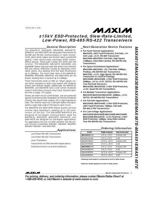
General DescriptionThe MAX3388E/MAX3389E are 2.5V-powered EI A/TI A-232 and V.28/V.24 communications interfaces with low power requirements, high data-rate capabilities, and enhanced electrostatic discharge (ESD) protection. The MAX3388E/MAX3389E have two receivers and three transmitters. All RS-232 inputs and outputs are protected to ±15kV using the I EC 1000-4-2 Air-Gap Discharge method, ±8kV using the IEC 1000-4-2 Contact Discharge method, and ±15kV using the Human Body Model.In addition to the traditional RS-232 I/O, these devices have dedicated logic-level I/O pins for additional device-to-device handshaking. During shutdown the logic-level I/O pins are active for the MAX3389E. An internal 62Ωswitch is provided to switch power to external circuitry or modules.A proprietary low-dropout transmitter output stage enables RS-232 compatible performance from a +2.35V to +3.0V supply with a dual charge pump. The charge pump requires only four small 0.1µF capacitors for oper-ation from a +2.5V supply. The MAX3388E/MAX3389E are capable of running at data rates up to 460kbps while maintaining RS-232-compatible output levels.The MAX3388E/MAX3389E have a unique V L pin that allows interoperation in mixed-logic voltage systems.Both input and output logic levels are pin programma-ble through the V L pin. The MAX3388E/MAX3389E are available in a space-saving TSSOP package.Featureso V L Pin for Compatibility with Mixed-Voltage Systemso Additional I/O for Hot-Sync Applicationso ±15kV ESD Protection on Rx Inputs, Tx Outputs,LIN, and SWINo Low 300µA Supply Current o Guaranteed 460kbps Data Rate o 1µA Low-Power Shutdowno Integrated Switch for Powering Remote Circuitry o Flow-Through Pinouto L OUT Active During Shutdown (MAX3389E)ApplicationsSubnotebook/Palmtop Computers PDAs and PDA Cradles Cell Phone Data Cables Battery-Powered Equipment Hand-Held Equipment PeripheralsMAX3388E/MAX3389E2.5V , ±15kV ESD-Protected RS-232 Transceivers for PDAs and Cell Phones________________________________________________________________Maxim Integrated Products 1Typical Operating Circuit19-1845; Rev 1; 9/01Pin ConfigurationOrdering InformationCovered by U.S Patent numbers 4,636,930; 4,679,134;4,777,577; 4,797,899; 4,809,152; 4,897,774; 4,999,761.For pricing, delivery, and ordering information,please contact Maxim/Dallas Direct!at 1-888-629-4642, or visit Maxim’s website at .M A X 3388E /M A X 3389E2.5V , ±15kV ESD-Protected RS-232Transceivers for PDAs and Cell Phones 2_______________________________________________________________________________________ABSOLUTE MAXIMUM RATINGSDC ELECTRICAL CHARACTERISTICS(V CC = V L = +2.35V to +3.0V, C1–C4 = 0.1µF, T A = T MIN to T MAX , unless otherwise noted. Typical values are at V CC = V L = +2.5V,T A = +25°C.)Stresses beyond those listed under “Absolute Maximum Ratings” may cause permanent damage to the device. These are stress ratings only, and functional operation of the device at these or any other conditions beyond those indicated in the operational sections of the specifications is not implied. Exposure to absolute maximum rating conditions for extended periods may affect device reliability.Note 1:V+ and V- can have maximum magnitudes of 7V, but their absolute difference cannot exceed 13V.V CC to GND..............................................................-0.3V to +6V V L to GND...................................................-0.3V to (V CC + 0.3V)V+ to GND................................................................-0.3V to +7V V- to GND.................................................................+0.3V to -7V V+ + V- (Note 1)...............................................................+13V Input VoltagesT_IN, SHDN,LIN to GND.......................................-0.3V to +6V R_IN to GND.....................................................................±25V SWIN to GND...........................................-0.3V to (V CC + 0.3V)Output VoltagesT_OUT to GND...............................................................±13.2V R_OUT, SWOUT, LOUT to GND ................-0.3V to (V L + 0.3V)Short-Circuit Duration T_OUT to GND........................Continuous Continuous Power Dissipation (T A = +70°C)24-Pin TSSOP (derate 12.2mW/°C above +70°C)........975mW Operating Temperature RangesMAX338_ECUG ...................................................0°C to +70°C MAX338_EEUG.................................................-40°C to +85°C Junction Temperature......................................................+150°C Storage Temperature Range.............................-65°C to +150°C Lead Temperature (soldering, 10s).................................+300°CMAX3388E/MAX3389E2.5V , ±15kV ESD-Protected RS-232 Transceivers for PDAs and Cell Phones_______________________________________________________________________________________3(V CC = V L = +2.35V to +3.0V, C1–C4 = 0.1µF, T A = T MIN to T MAX , unless otherwise noted. Typical values are at V CC = V L = +2.5V,T= +25°C.)Note 3:Transmitter skew is measured at the transmitter zero crosspoint.DC ELECTRICAL CHARACTERISTICS (continued)(V CC = V L = +2.35V to +3.0V, C1–C4 = 0.1µF, T A = T MIN to T MAX , unless otherwise noted. Typical values are at V CC = V L = +2.5V,M A X 3388E /M A X 3389E2.5V , ±15kV ESD-Protected RS-232Transceivers for PDAs and Cell Phones 4_______________________________________________________________________________________Typical Operating Characteristics(V CC = V L = +2.5V, T A = +25°C, unless otherwise noted.)-5.0-2.52.55.0020001000300040005000TRANSMITTER OUTPUT VOLTAGEvs. LOAD CAPACITANCELOAD CAPACITANCE (pF)O U T P U T V O L T A G E (V )024681012141610002000300040005000SLEW RATE vs. LOAD CAPACITANCELOAD CAPACITANCE (pF)S L E W R A T E (V /µs )-5.0-2.52.55.0010015020025050300350400450TRANSMITTER OUTPUT VOLTAGEvs. DATA RATEDATA RATE (kbps)O U T P U T V O L T A G E (V )0201040305060020001000300040005000SUPPLY CURRENT vs. LOAD CAPACITANCELOAD CAPACITANCE (pF)S U P P L Y C U R R E N T (m A )M A X 3388E t o c 05200ns/divR PULLUP = 1k ΩMAX3388E/MAX3389E2.5V , ±15kV ESD-Protected RS-232 Transceivers for PDAs and Cell Phones_______________________________________________________________________________________5M A X 3388E /M A X 3389E2.5V , ±15kV ESD-Protected RS-232Transceivers for PDAs and Cell Phones 6_______________________________________________________________________________________Detailed DescriptionDual Charge-Pump Voltage ConverterThe MAX3388E/MAX3389E ’s internal power supply consists of a regulated dual charge pump that provides output voltages of +4.2V (doubling charge pump) and -4.2V (inverting charge pump), regardless of the input voltage (V CC ) over a +2.5V to +3.0V range. The charge pumps operate in a discontinuous mode: if the output voltages are less than 4.2V, the charge pumps are enabled; if the output voltages exceed 4.2V, the charge pumps are disabled. Each charge pump requires flying capacitors (C1, C2) and reservoir capacitors (C3, C4)to generate the V+ and V- supplies.RS-232 TransmittersThe transmitters are inverting level translators that convert CMOS-logic levels to ±3.7V EI A/TI A-232-compatible levels.The MAX3388E/MAX3389E ’s transmitters guarantee a 250kbps data rate with loads of 3k Ωin parallel with 1000pF and 460kbps data rate with loads of 3k lel with 150pF. Figure 1 shows a complete system con-nection.These RS-232 output stages are turned off (high impedance) when the devices are in shutdown mode.When the power is off, the MAX3388E/MAX3389E permit the outputs to be driven up to ±12V.The transmitter inputs do not have pullup resistors.Connect unused inputs to GND or V L .RS-232 ReceiversThe receivers convert RS-232 signals to CMOS-logic output levels. The MAX3388E/MAX3389E ’s receivers have inverting outputs. The outputs are high imped-ance in shutdown.Shutdown ModeSupply current falls to less than 1µA when the MAX3388E/MAX3389E are placed in shutdown mode (SHDN logic low). When shut down, the device ’s charge pumps are turned off, V+ decays to V CC , V- is pulled to ground, the switch is opened, and the transmitter outputs are disabled (high impedance). The time required to exitFigure 1. Interface Under Control of PMU10µs/divV CC = +2.5V C1–C4 = 0.1µFC L = 1000pF, R L = 3k ΩFigure 2. Transmitter Outputs when Exiting ShutdownMAX3388E/MAX3389E2.5V , ±15kV ESD-Protected RS-232 Transceivers for PDAs and Cell Phones_______________________________________________________________________________________7shutdown is typically 30µs, as shown in Figure 2.Connect SHDN to V CC if the shutdown mode is not used.In shutdown mode, the receiver outputs are high imped-ance (Table 1).V L Logic Supply InputUnlike other RS-232 interface devices where the receiver outputs swing between 0 and V CC , the MAX3388E/MAX3389E feature a separate logic supply input (V L )that sets V OH for the receiver outputs and sets thresh-olds for the transmitter inputs. This feature allows a great deal of flexibility in interfacing to many different types of systems with different logic levels. Connect this input to the host logic supply (1.8V ≤V L ≤V CC ).Also see the Typical PDA/Cell-Phone Application sec-tion.±15kV ESD ProtectionAs with all Maxim devices, ESD-protection structures are incorporated on all pins to protect against ESDs encoun-tered during handling and assembly. The MAX3388E/MAX3389E ’s driver outputs, receiver inputs, the hand-shaking input LI N, and the switch terminal SWI N have extra protection against static electricity. Maxim has developed state-of-the-art structures to protect these pins against an ESD of ±15kV without damage. The ESD structures withstand high ESD in all states: normal opera-tion, shutdown, and powered down. After an ESD event,Maxim ’s “E ” version devices keep working without latchup, whereas competing RS-232 products can latch and must be powered down to remove latchup. ESD pro-tection can be tested in various ways. The transmitter out-puts and receiver inputs of this product family are characterized for protection to the following limits:1)±15kV using the Human Body Model2)±8kV using the Contact Discharge method specified in IEC 1000-4-23)±15kV using I EC 1000-4-2’s Air-Gap Discharge methodESD Test ConditionsESD performance depends on a variety of conditions.Contact Maxim for a reliability report that documents test setup, methodology, and results.Human Body ModelFigure 3a shows the Human Body Model, and Figure 3b shows the current waveform it generates when dis-charged into a low impedance. This model consists of a 100pF capacitor charged to the ESD voltage of interest,which is then discharged into the test device through a 1.5k Ωresistor.IEC 1000-4-2The I EC 1000-4-2 standard covers ESD testing and performance of finished equipment; it does not specifi-cally refer to ICs. The MAX3388E/MAX3389E helps you design equipment that meets Level 4 (the highest level)of I EC 1000-4-2, without the need for additional ESD-protection components.The major difference between tests done using the Human Body Model and I EC 1000-4-2 is higher peak current in I EC 1000-4-2, because series resistance is lower in the IEC 1000-4-2 model. Hence, the ESD with-stand voltage measured to I EC 1000-4-2 is generally lower than that measured using the Human Body Model. Figure 4a shows the I EC 1000-4-2 model, and Figure 4b shows the current waveform for the ±8kV IEC 1000-4-2 Level 4 ESD Contact Discharge test.Figure 3a. Human Body ESD Test ModelFigure 3b. Human Body Current WaveformThe Air-Gap test involves approaching the device with a charged probe. The contact discharge method connects the probe to the device before the probe is energized.Machine ModelThe Machine Model for ESD tests all pins using a 200pF storage capacitor and zero discharge resis-tance. Its objective is to emulate the stress caused by contact that occurs with handling and assembly during manufacturing. All pins require this protection during manufacturing, not just RS-232 inputs and outputs.Therefore, after PC board assembly, the Machine Model is less relevant to I/O ports.__________Applications InformationCapacitor SelectionThe capacitor type used for C1–C4 is not critical for proper operation; polarized or nonpolarized capacitors can be used. The charge pump requires 0.1µF capacitors for 2.5V operation (Table 2). Do not use values smaller than those listed in Table 2. I ncreasing the capacitor values (e.g., by a factor of 2) reduces ripple on the transmitter outputs and slightly reduces power con-sumption. C2, C3, and C4 can be increased without changing C1’s value. However, do not increase C1without also increasing the values of C2, C3, and C4 to maintain the proper ratios (C1 to the other capacitors).When using the minimum required capacitor values,make sure the capacitor value does not degrade excessively with temperature. If in doubt, use capacitors with a larger nominal value. The capacitor ’s equivalent series resistance (ESR), which usually rises at low tem-peratures, influences the amount of ripple on V+ and V-.Power-Supply DecouplingI n most circumstances, a 0.1µF bypass capacitor is adequate.In applications that are sensitive to power-supply noise, decouple V CC to ground with a capacitor of the same value as charge-pump capacitor C1. Connect bypass capacitors as close to the IC as possible.Transmitter Outputs whenExiting ShutdownFigure 2 shows two transmitter outputs when exiting shutdown mode. As they become active, the two transmitter outputs are shown going to opposite RS-232levels (one transmitter input is high; the other is low).Each transmitter is loaded with 3k Ωin parallel with 1000pF. The transmitter outputs display no ringing or undesirable transients as they come out of shutdown.Note that the transmitters are enabled only when the magnitude of V- exceeds approximately 2.5V.M A X 3388E /M A X 3389E2.5V , ±15kV ESD-Protected RS-232Transceivers for PDAs and Cell Phones 8_______________________________________________________________________________________Figure 4a. IEC 1000-4-2 ESD Test ModelFigure 4b. IEC 1000-4-2 ESD Generator Current WaveformTable 2. Minimum Required Capacitor ValuesMAX3388E/MAX3389E2.5V , ±15kV ESD-Protected RS-232 Transceivers for PDAs and Cell PhonesHigh Data RatesThe MAX3388E/MAX3389E maintain RS-232-compatible transmitter output voltages even at high data rates. Figure 5 shows a transmitter loopback test circuit. Figure 6shows a loopback test result at 250kbps, and Figure 7 shows the same test at 460kbps. For Figure 6, all transmitters were driven simultaneously at 250kbps into RS-232 loads in parallel with 1000pF. For Figure 7, a single transmitter was driven at 460kbps, and all transmitters were loaded with an RS-232 receiver in parallel with 150pF.Power SwitchThe MAX3388E/MAX3389E contain an internal switch for powering external circuitry. This can be used to power hot-sync circuitry or other low-power circuitry.The switch on- resistance is typically 62Ω. The SWI N side of the switch is ESD protected to ±15kV.Logic-Level I/On addition to the traditional RS-232 I /O, the MAX3388E/MAX3389E have a logic-level transceiver from the RS-232 connector side to the CMOS-logic side. The input impedance is typically 30k Ω, and the output is open drain. The logic level I/O is active during shutdown for the MAX3389E.This I /O transceiver is useful for hot syncing or other dedicated communication capability. The input is ESD protected to ±15kV.Typical PDA/Cell-Phone ApplicationThe MAX3388E/MAX3389E designed with PDA applica-tions in mind. Two transmitters and two receivers handle standard full-duplex communication protocol, while an extra transmitter allows a ring indicator (RI) signal to alert the UART on the PC. Without the ring indicator transmit-ter, solutions for these applications would require soft-ware-intensive polling of the cradle inputs.The RI signal is generated when a PDA, cellular phone, or other “cradled ” device is plugged into its cradle. This generates a logic-low signal to RI transmitter input, creat-ing +3.7V at the ring indicate pin. The PC ’s UART RI input is the only pin that can generate an interrupt from signals arriving through the RS-232 port. The interrupt routine for this UART will then service the RS-232 full-duplex com-munication between the PDA and the PC.As cell phone design becomes more like that of PDAs,cell phones will require similar docking ability and com-munication protocol. Cell phones operate on a single lithium-ion (Li+) battery and generate a regulated out-put voltage of +2.35V to +3V from the phone connector.The baseband logic coming from the phone connector can be as low as 1.8V at the transceivers. To prevent forward biasing of a device internal to the cell phone,the MAX3388E/MAX3389E come with a logic power-supply pin (V L ) that limits the logic levels presented toFigure 5. Loopback Test Circuit1µs/divC L = 1000pFFigure 6. Loopback Test Results at 250kbps_______________________________________________________________________________________9the phone. The receiver outputs will sink to zero for low outputs, but will not exceed V L for logic highs. The input logic levels for the transmitters are also altered,scaled by the magnitude of the V L input. The devices will work with V L as low as 1.8V. This is useful with cell phones and other power-efficient devices with core logic voltage levels that go as low as 1.8V.Chip InformationTRANSISTOR COUNT: 1323M A X 3388E /M A X 3389E2.5V , ±15kV ESD-Protected RS-232Transceivers for PDAs and Cell Phones 10______________________________________________________________________________________1µs/divC L = 150pFFigure 7. Loopback Test Results at 460kbpsMAX3388E/MAX3389E 2.5V , ±15kV ESD-Protected RS-232 Transceivers for PDAs and Cell PhonesMaxim cannot assume responsibility for use of any circuitry other than circuitry entirely embodied in a Maxim product. No circuit patent licenses are implied. Maxim reserves the right to change the circuitry and specifications without notice at any time.Maxim Integrated Products, 120 San Gabriel Drive, Sunnyvale, CA 94086 408-737-7600_____________________11©2001 Maxim Integrated Products Printed USA is a registered trademark of Maxim Integrated Products.元器件交易网。