集成电路封装和可靠性Chapter芯片互连技术
- 格式:pdf
- 大小:4.06 MB
- 文档页数:81
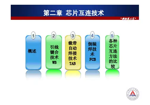
*微组装工艺*2引线键合技术WB 3载带自动焊接技术TAB 第二章芯片互连技术1概述4倒装焊技术FCB 5各种芯片互连方法的比较*微组装工艺*2.1概述芯片互连技术是将芯片直接与基板相连接的一种技术。
主要包括引线键合、载带自动焊接、倒装芯片技术。
半导体封装内部芯片和外部管脚以及芯片之间的连接起着确立芯片和外部的电气连接、确保芯片和外界之间的输入/ 输出畅通的重要作用,是整个后道封装过程中的关键。
半导体器件的失效约有1/4~1/3是由芯片互连引起的,芯片互连技术对器件长期使用的可靠性影响很大。
*微组装工艺*WB,TAB,FCB不单主要作为芯片—基板间的电气互连形式,而且还作为一种微电子封装形式,常称为“零级”封装。
从微电子封装今后的发展来看,将从有封装向少封装、无封装方向发展。
而无封装就是通常的裸芯片,若将这种无封装的裸芯片用WB,TAB,FCB的芯片互连方式直接安装到基板上,即称为板上芯片(COB)和板上TAB或板上FCB,这些统称为直接芯片安装(DCA)技术,它将在今后的微电子封装中发挥更重要的作用。
2.2 引线键合技术2.2.12.2.22.2.52.2.6*微组装工艺*一、引线键合技术引线键合技术是将半导体裸芯片(Die )焊区与微电子封装的I/O 引线或基板上的金属布线焊区(Pad )用金属细丝连接起来的工艺技术。
工作原理:提供能量破坏被焊表面的氧化层和污染物,使焊区金属产生塑性变形,使得引线与被焊面紧密接触,达到原子间引力范围并导致界面间原子扩散而形成焊合点。
焊区金属一般为AL 或Au 金属丝。
多数是1微米至数百微米直径的Au 丝、AL 丝和Si-AL 丝。
2.2.1 引线键合技术*微组装工艺*布线端子*微组装工艺*引线键合技术的特点:引线键合以工艺实现简单、成本低廉、适用多种封装形式而在连接方式中占主导地位。
引线键合技术适用于几乎所有的半导体集成电路元件,操作方便,封装密度高。
低成本、高可靠、高产量等特点使得WB成为芯片互连主要工艺方法,但引线长、压焊过重、测试性差等问题容易引起互连失效。
UESTC-Ning Ning1Chapter 2Chip Level Interconnection宁宁芯片互连技术集成电路封装测试与可靠性UESTC-Ning Ning2Wafer InWafer Grinding (WG 研磨)Wafer Saw (WS 切割)Die Attach (DA 黏晶)Epoxy Curing (EC 银胶烘烤)Wire Bond (WB 引线键合)Die Coating (DC 晶粒封胶/涂覆)Molding (MD 塑封)Post Mold Cure (PMC 模塑后烘烤)Dejunk/Trim (DT 去胶去纬)Solder Plating (SP 锡铅电镀)Top Mark (TM 正面印码)Forming/Singular (FS 去框/成型)Lead Scan (LS 检测)Packing (PK 包装)典型的IC 封装工艺流程集成电路封装测试与可靠性UESTC-Ning Ning3⏹电子级硅所含的硅的纯度很高,可达99.9999 99999 %⏹中德电子材料公司制作的晶棒(长度达一公尺,重量超过一百公斤)UESTC-Ning Ning4Wafer Back Grinding⏹PurposeThe wafer backgrind process reduces the thickness of the wafer produced by silicon fabrication (FAB) plant. The wash station integrated into the same machine is used to wash away debris left over from the grinding process.⏹Process Methods:1) Coarse grinding by mechanical.(粗磨)2) Fine polishing by mechanical or plasma etching. (细磨抛光)UESTC-Ning Ning5旋转及振荡轴在旋转平盘上之晶圆下压力工作台仅在指示有晶圆期间才旋转Method:The wafer is first mounted on a backgrind tape and is then loaded to the backgrind machine coarse wheel . As the coarse grinding is completed, the wafer is transferred to a fine wheel for polishing .。
一、填空题1、将芯片及其他要素在框架或基板上布置,粘贴固定以及连接,引出接线端子并且通过可塑性绝缘介质灌封固定的过程为狭义封装;在次根基之上,将封装体与装配成完整的系统或者设备,这个过程称之为广义封装。
2、芯片封装所实现的功能有传递电能;传递电路信号;提供散热途径;构造保护与支持。
3、芯片封装工艺的流程为硅片减薄与切割、芯片贴装、芯片互连、成型技术、去飞边毛刺、切筋成形、上焊锡、打码。
4、芯片贴装的主要方法有共晶粘贴法、焊接粘贴法、导电胶粘贴发、玻璃胶粘贴法。
5、金属凸点制作工艺中,多金属分层为黏着层、扩散阻挡层、表层金保护层。
6、成型技术有多种,包括了转移成型技术、喷射成型技术、预成型技术、其中最主要的是转移成型技术。
7、在焊接材料中,形成焊点完成电路电气连接的物质叫做煤斜;;用于去除焊盘外表氧化物,提高可焊性的物质叫做助焊剂;在SMT中常用的可印刷焊接材料叫做锡直。
8、气密性封装主要包括了金属气密性封装、陶瓷气密性封装、玻璃气密性封装。
9、薄膜工艺主要有遮射工艺、蒸发工艺、电镀工艺、光刻工艺。
10、集成电路封装的层次分为四级分别为模块元件(MOdUIe)、⅛路卡工艺(Card)、主电路板(Board)、完整电子产品。
11、在芯片的减薄过程中,主要方法有磨削、研磨、干式抛光、化学机械平坦工艺、电化学腐蚀、湿法腐蚀、等离子增强化学腐蚀等。
12、芯片的互连技术可以分为打线键合技术、载带自动键合技术、倒装芯片键合技术。
13、DBG切割方法进展芯片处理时,首先进展在硅片正面切割一定深度切口再进展反面磨削。
14、膜技术包括了薄膜技术和厚膜技术,制作较厚薄膜时常采用丝网印刷和浆料枯燥烧结的方法O15、芯片的外表组装过程中,焊料的涂覆方法有点涂、丝网印刷、钢模板印刷三种。
16、涂封技术一般包括了顺形涂封和封胶涂封。
二、名词解释1、芯片的引线键合技术(3种)是将细金属线或金属带按顺序打在芯片与引脚架或封装基板的焊垫上而形成电路互连,包括超声波键合、热压键合、热超声波键合。

1.引言任何一个电子元件,不论是一个三极管还是一个集成电路(Integrated Circuit, IC),想要使用它,都需要把它连入电路里。
一个三极管,只需要在源极、漏极、栅极引出三根线就可以了,然而对于拥有上百或上千个引脚的超大规模集成电路(Very Large Scale Integration Circuit, VLSI)来说,靠这种类似于手动把连线插到面包板的过程是不可能的。
直接把IC连接到(未经封装的集成电路本体,裸片,Die)电路中也是不可能实现的,因为裸片极容易收到外界的温度、杂质和外力的影响,非常容易遭到破坏而失效。
所以电子封装的主要目的就是提供芯片与其他电子元器件的互连以实现电信号的传输,同时提供保护,以便于将芯片安装在电路系统中。
一般的半导体封装都类似于下面的结构,将裸片安装到某个基板上,裸片的引脚通过内部连接路径与基板相连,通过塑封将内部封装好后,基板再通过封装提供的外部连接路径与外部电路相连,实现内部芯片与外界的连接,就像上面两个图一样,裸Die和封装内部复杂的连接等都埋在里面,封装好后就是对外就是一些规整的引脚了。
不论是多复杂的封装,从黑盒的角度来看其实现的基本功能都是一样的,最简单的就是封装一个分立器件,给出几个引脚;复杂一点想要封装具有多个I/O 接口的IC,以及多个IC一起封装,在封装的发展过程中也发展出了很多封装类型和很多技术,比如扇出技术、扇入技术这些。
这些概念和缩写非常多,尤其是当谈到先进封装(Advanced Packaging)的时候,为了实现高密度集成以及快速信号传输这些需求,不得不在每一个地方都发展一些新的技术,很多情况下会把它们都并入到先进封装技术里来介绍,这有时候会引起一些困惑,这里主要整理一下IC封装里的互连技术。
在IC封装种几种典型的互连技术包括引线键合(Wire Bonding,WB)、载带自动焊(Tape-automated Bonding,TAB)、倒装芯片(Flip Chip,FC)、晶圆级封装(Wafer-Level Packaging,WLP)、以及硅通孔(Through Silicon Via,TSV)。
封装互连技术是一种将集成电路和外部电路连接在一起的技术,它包括引脚插装、倒装焊、载带自动焊、超声键合等。
这些技术可以用来将集成电路封装在印刷电路板、陶瓷或其他类型的基板上,以实现电路的集成化和小型化。
在封装互连技术中,引脚插装是最常见的一种。
它使用金属引脚将集成电路与外部电路连接在一起。
这种技术可以提供较好的电气性能和可靠性,因此在许多领域得到广泛应用。
倒装焊是一种将集成电路直接焊在基板上的技术,不需要使用引脚。
这种技术可以减小封装体积,提高封装密度,因此被广泛应用于便携式电子设备和移动通信领域。
载带自动焊是一种将集成电路放置在塑料或陶瓷载带上,然后通过焊接将载带与外部电路连接在一起的技术。
这种技术可以提供高速度、高精度和高可靠性的封装互连,因此在许多高可靠性领域得到广泛应用。
超声键合是一种利用超声波能量将两个金属表面连接在一起的技术。
这种技术可以提供高可靠性和高稳定性的封装互连,因此在许多高可靠性领域得到广泛应用。
总的来说,封装互连技术是实现电路集成化和小型化的关键技术之一。
随着电子设备的发展,对封装互连技术的要求也越来越高,需要不断改进和创新。
UESTC-Ning Ning1Chapter 2Chip Level Interconnection宁宁芯片互连技术集成电路封装测试与可靠性UESTC-Ning Ning2Wafer InWafer Grinding (WG 研磨)Wafer Saw (WS 切割)Die Attach (DA 黏晶)Epoxy Curing (EC 银胶烘烤)Wire Bond (WB 引线键合)Die Coating (DC 晶粒封胶/涂覆)Molding (MD 塑封)Post Mold Cure (PMC 模塑后烘烤)Dejunk/Trim (DT 去胶去纬)Solder Plating (SP 锡铅电镀)Top Mark (TM 正面印码)Forming/Singular (FS 去框/成型)Lead Scan (LS 检测)Packing (PK 包装)典型的IC 封装工艺流程集成电路封装测试与可靠性UESTC-Ning Ning3⏹电子级硅所含的硅的纯度很高,可达99.9999 99999 %⏹中德电子材料公司制作的晶棒(长度达一公尺,重量超过一百公斤)UESTC-Ning Ning4Wafer Back Grinding⏹PurposeThe wafer backgrind process reduces the thickness of the wafer produced by silicon fabrication (FAB) plant. The wash station integrated into the same machine is used to wash away debris left over from the grinding process.⏹Process Methods:1) Coarse grinding by mechanical.(粗磨)2) Fine polishing by mechanical or plasma etching. (细磨抛光)UESTC-Ning Ning5旋转及振荡轴在旋转平盘上之晶圆下压力工作台仅在指示有晶圆期间才旋转Method:The wafer is first mounted on a backgrind tape and is then loaded to the backgrind machine coarse wheel . As the coarse grinding is completed, the wafer is transferred to a fine wheel for polishing .UESTC-Ning Ning6 Wafer Back Grinding processObjective:To reduce thethicknesswith a coarse grindingwheel.Objective:To load and alignthe wafer into thewafer cleaning andtape laminationmachine.Objective:To clean the waferfor the nextlamination step.Objective:To laminate a protectivelayer of film on thecircuitry surface of thewafer .2. Wafer cleaning1. Load and Align 3. Back grind Tape lamination4. Coarse grindingUESTC-Ning Ning7Wafer Back Grinding process (Cont.)Objective:To unload the wafer from back grinding machine.5. Fine polishing6. UnloadObjective:To load the wafer to wafer mounter.Objective:To remove the back grind tape afterwafer mounted on the frame.8. Tape removal7. LoadUESTC-Ning Ning8Wafer Back Grinding Issues and Challenges⏹Issues☐Ease of process–Thin wafer handling from one step to another –Back grinding tape removal–Excessive stresses removal or reduction from the wafer.(应力)☐Yield–Wafer breakage due to stress built up during thinning process. –Scratches .(划痕)–Die metallization smearing.(污点,模糊)☐Equipment stability and capability⏹Challenges☐Market requirements drive for very thin wafer (<3 mils)☐Flip chip wafer back grindingUESTC-Ning Ning9Wafer sawing⏹Wafer Separation Process►Purpose:The wafer separation process is to divide the wafer into individual dice or chips.Process Methods:1)Sawing (with diamond-impregnated saw blade) 锯切☐Single or dual cut ☐Step cut or bevel cut2) Partial scribing (with laser beam, diamond-tipped scribing tool, or diamond-impregnated saw blade) 局部划片器UESTC-Ning Ning10Wafer sawingUESTC-Ning Ning11►Wafer Sawing is a Front-of-Line (FOL) operation that cuts the wafer along the streets separating the individual die. Streets, also called scribe lines , are lines on the wafer that separate each individual die from the surrounding dice. Kerf width is the saw width. After the wafer is sawn, the wash station, using a detergent, removes residual cut material fromthe wafer.Wafer sawingDicing Blade晶圆工作台刀刃NingUESTC-Ning Ning13The SAWING process is broken down into four steps:Objective:To rinse slurry (silicon dust)before it dries with de-ionized water and CO2. Also to drywafer by pinning and with clean air , and unload wafer .1. Load and Align2. Pattern Recognition System (PRS)3. Cut4. Wash, Rinse, Dry and UnloadObjective:To separate dice from a wafer with resin-bonded diamond wheel . (First blade is used to remove metal structures and stresses on street for second blade.)Wafer sawingUESTC-Ning Ning14Wafer Sawing Issues and Challenges⏹Issues:☐Ease of process--Die chipping control (碎屑)--Multiple die types and sizes processing☐Yield--Saw on die--Scratches (划痕)--Chipping --Die crack☐Equipment stability and capability⏹Challenges:☐Smaller kerf width for more die per wafer☐Larger wafer size (300mm)with multiple die types and sizesUESTC-Ning Ning15--Die Attach Process☐Purpose:The die attach process is to attach the sawed die in the right orientation accurately onto the substrate with a bonding medium in between to enable the next wire bond first level interconnection operation .☐Process Methods1)Semi-automated eutectic die attach .低共熔物芯片粘接2)Fully automated adhesive die attach.胶粘剂粘接--Die Attach Process 晶粒--Die Attach Process☐Au-Si 低共熔合金粘接法金膜◆低共融合金粘接法主要用在芯片产品需要非常低的背部接触电阻。
UESTC-Ning Ning1Chapter 2Chip Level Interconnection宁宁芯片互连技术集成电路封装测试与可靠性UESTC-Ning Ning2Wafer InWafer Grinding (WG 研磨)Wafer Saw (WS 切割)Die Attach (DA 黏晶)Epoxy Curing (EC 银胶烘烤)Wire Bond (WB 引线键合)Die Coating (DC 晶粒封胶/涂覆)Molding (MD 塑封)Post Mold Cure (PMC 模塑后烘烤)Dejunk/Trim (DT 去胶去纬)Solder Plating (SP 锡铅电镀)Top Mark (TM 正面印码)Forming/Singular (FS 去框/成型)Lead Scan (LS 检测)Packing (PK 包装)典型的IC 封装工艺流程集成电路封装测试与可靠性UESTC-Ning Ning3⏹电子级硅所含的硅的纯度很高,可达99.9999 99999 %⏹中德电子材料公司制作的晶棒(长度达一公尺,重量超过一百公斤)UESTC-Ning Ning4Wafer Back Grinding⏹PurposeThe wafer backgrind process reduces the thickness of the wafer produced by silicon fabrication (FAB) plant. The wash station integrated into the same machine is used to wash away debris left over from the grinding process.⏹Process Methods:1) Coarse grinding by mechanical.(粗磨)2) Fine polishing by mechanical or plasma etching. (细磨抛光)UESTC-Ning Ning5旋转及振荡轴在旋转平盘上之晶圆下压力工作台仅在指示有晶圆期间才旋转Method:The wafer is first mounted on a backgrind tape and is then loaded to the backgrind machine coarse wheel . As the coarse grinding is completed, the wafer is transferred to a fine wheel for polishing .UESTC-Ning Ning6 Wafer Back Grinding processObjective:To reduce thethicknesswith a coarse grindingwheel.Objective:To load and alignthe wafer into thewafer cleaning andtape laminationmachine.Objective:To clean the waferfor the nextlamination step.Objective:To laminate a protectivelayer of film on thecircuitry surface of thewafer .2. Wafer cleaning1. Load and Align 3. Back grind Tape lamination4. Coarse grindingUESTC-Ning Ning7Wafer Back Grinding process (Cont.)Objective:To unload the wafer from back grinding machine.5. Fine polishing6. UnloadObjective:To load the wafer to wafer mounter.Objective:To remove the back grind tape afterwafer mounted on the frame.8. Tape removal7. LoadUESTC-Ning Ning8Wafer Back Grinding Issues and Challenges⏹Issues☐Ease of process–Thin wafer handling from one step to another –Back grinding tape removal–Excessive stresses removal or reduction from the wafer.(应力)☐Yield–Wafer breakage due to stress built up during thinning process. –Scratches .(划痕)–Die metallization smearing.(污点,模糊)☐Equipment stability and capability⏹Challenges☐Market requirements drive for very thin wafer (<3 mils)☐Flip chip wafer back grindingUESTC-Ning Ning9Wafer sawing⏹Wafer Separation Process►Purpose:The wafer separation process is to divide the wafer into individual dice or chips.Process Methods:1)Sawing (with diamond-impregnated saw blade) 锯切☐Single or dual cut ☐Step cut or bevel cut2) Partial scribing (with laser beam, diamond-tipped scribing tool, or diamond-impregnated saw blade) 局部划片器UESTC-Ning Ning10Wafer sawingUESTC-Ning Ning11►Wafer Sawing is a Front-of-Line (FOL) operation that cuts the wafer along the streets separating the individual die. Streets, also called scribe lines , are lines on the wafer that separate each individual die from the surrounding dice. Kerf width is the saw width. After the wafer is sawn, the wash station, using a detergent, removes residual cut material fromthe wafer.Wafer sawingDicing Blade晶圆工作台刀刃NingUESTC-Ning Ning13The SAWING process is broken down into four steps:Objective:To rinse slurry (silicon dust)before it dries with de-ionized water and CO2. Also to drywafer by pinning and with clean air , and unload wafer .1. Load and Align2. Pattern Recognition System (PRS)3. Cut4. Wash, Rinse, Dry and UnloadObjective:To separate dice from a wafer with resin-bonded diamond wheel . (First blade is used to remove metal structures and stresses on street for second blade.)Wafer sawingUESTC-Ning Ning14Wafer Sawing Issues and Challenges⏹Issues:☐Ease of process--Die chipping control (碎屑)--Multiple die types and sizes processing☐Yield--Saw on die--Scratches (划痕)--Chipping --Die crack☐Equipment stability and capability⏹Challenges:☐Smaller kerf width for more die per wafer☐Larger wafer size (300mm)with multiple die types and sizesUESTC-Ning Ning15--Die Attach Process☐Purpose:The die attach process is to attach the sawed die in the right orientation accurately onto the substrate with a bonding medium in between to enable the next wire bond first level interconnection operation .☐Process Methods1)Semi-automated eutectic die attach .低共熔物芯片粘接2)Fully automated adhesive die attach.胶粘剂粘接--Die Attach Process 晶粒--Die Attach Process☐Au-Si 低共熔合金粘接法金膜◆低共融合金粘接法主要用在芯片产品需要非常低的背部接触电阻。
--Die Attach ProcessUESTC-Ning Ning19--Die Attach ProcessUESTC-Ning Ning20 1. Units and Dice/ wafer LoadObjective:To load the carrierswith the units placedon them. To loadthe dice/wafer intothe machine.2. Bonding Medium DispenseObjective:To dispense thebonding mediumonto the substratedie attach paddle.3. Pattern Recognition System(PRS) & AlignObjective:To align the theta(rotation) position ofthe wafer. To align thedie (X-Y)with respectto the package PRSeye points.4. Die AttachObjective:To attach the dieprecisely and form agood adhesion withdesired bond linethickness (BLT).--Die Attach Process--Die Attach Process 5. Unload (Die Attach)UESTC-Ning Ning22Wire Bonding Technology Die Attach ProcessIssues and Challenges☐Issues:◆Ease of process–Delamination control –Void control ◆Yield–Adhesive on die–Incomplete wet out/fillet –Die crack–Die placement◆Equipment stability and capability☐Challenges:◆Market requirements drive for very thin die (<3 mils).◆Material selection (e.g. lead free compatible, thermal Materialselection and electrical requirements).UESTC-Ning Ning23--Wire Bonding ProcessUESTC-Ning Ning245. UnloadObjective:To unload the carriers after wire bond.To unload the wire spool when the wireis used upThe Wire Bonding Process --Wire Bonding ProcessUESTC-Ning Ning25Wire Bonding Issues and Challenges◆Challenges:☐Market requirements drive for tighter bond pitch . (<37/75um staggered , <60um non-staggered).☐Smaller wire diameter (<1.0mils).☐Brittle Intermetallic composition (IMC) on lead free.◆Issues:☐Ease of process-Looping profile control.-Process optimization for bond ability and bond reliability.☐Yield-Lifted bond (non stick on pad or lead).-Sagging and swayed wire. 引线塌陷或歪斜-Tight loop.☐Equipment stability and capability.交错排列无铅工艺中易脆的金属间化合物UESTC-Ning Ning26 MD(封塑)(Molding)BM(背印)(Back Mark)D/T(去胶/去纬)(Dejunk/Trim)SP(电镀)(Solder Panting)F/S(成型/去框)(Form/Singulation)F/T(功能测试)(Function/Test)PK(包装)(Packing)PMC(烘烤)(Post Mold Cure)MC(烘烤)(Mark Cure)TM(正印)(Top Mark)LS(检测)(lead Scan)Molding塑封成型UESTC-Ning Ning27按封装材料分类:陶瓷封裝常用于特殊用途和专业领域IC芯片例如:高频和军事通讯加盖式气密性封装UESTC-Ning NingUESTC-Ning Ning29☐Hermetic lid Sealing在第一级互连完成后,将周围印刷有焊料的盖子(或陶瓷,金属或塑料盖)放置在封装基板腔体上(芯片已键合在腔体内)。