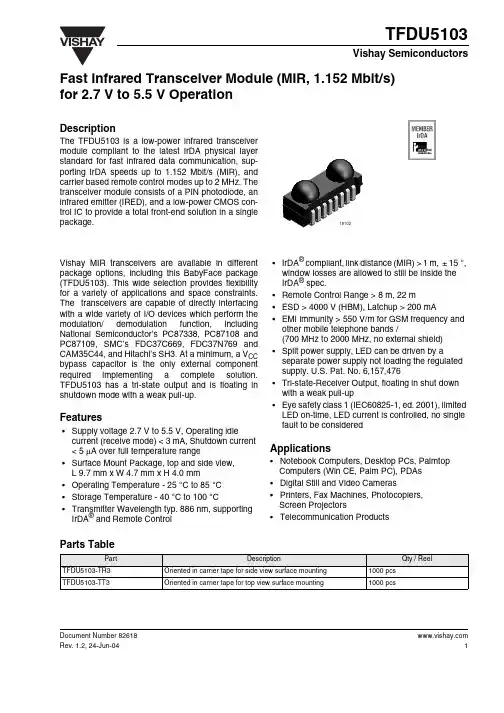
Document Number 82618 18102Fast Infrared Transceiver Module (MIR, 1.152 Mbit/s) for 2.7 V to 5.5 V OperationDescriptionThe TFDU5103 is a low-power infrared transceivermodule compliant to the latest IrDA physical layerstandard for fast infrared data communication, sup-porting IrDA speeds up to 1.152 Mbit/s (MIR), andcarrier based remote control modes up to 2 MHz. Thetransceiver module consists of a PIN photodiode, aninfrared emitter (IRED), and a low-power CMOS con-trol IC to provide a total front-end solution in a singlepackage.Vishay MIR transceivers are available in different package options, including this BabyFace package (TFDU5103). This wide selection provides flexibility for a variety of applications and space constraints. The transceivers are capable of directly interfacing with a wide variety of I/O devices which perform the modulation/ demodulation function, including National Semiconductor’s PC87338, PC87108 and PC87109, SMC’s FDC37C669, FDC37N769 and CAM35C44, and Hitachi’s SH3. At a minimum, a V CC bypass capacitor is the only external component required implementing a complete solution. TFDU5103 has a tri-state output and is floating in shutdown mode with a weak pull-up.Features•Supply voltage 2.7 V to 5.5 V, Operating idle current (receive mode) < 3 mA, Shutdown current < 5 µA over full temperature range•Surface Mount Package, top and side view, L 9.7 mm x W 4.7 mm x H 4.0 mm •Operating Temperature - 25°C to 85°C •Storage Temperature - 40°C to 100°C •Transmitter Wavelength typ. 886 nm, supporting IrDA® and Remote Control•IrDA® compliant, link distance (MIR) > 1 m, ± 15°, window losses are allowed to still be inside theIrDA® spec.•Remote Control Range > 8 m, 22 m•ESD > 4000 V (HBM), Latchup > 200 mA •EMI immunity > 550 V/m for GSM frequency and other mobile telephone bands /(700 MHz to 2000 MHz, no external shield) •Split power supply, LED can be driven by a separate power supply not loading the regulated supply. U.S. Pat. No. 6,157,476•Tri-state-Receiver Output, floating in shut down with a weak pull-up•Eye safety class 1 (IEC60825-1, ed. 2001), limited LED on-time, LED current is controlled, no single fault to be consideredApplications• Notebook Computers, Desktop PCs, PalmtopComputers (Win CE, Palm PC), PDAs• Digital Still and Video Cameras• Printers, Fax Machines, Photocopiers,Screen Projectors• Telecommunication ProductsParts TablePart Description Qty / Reel TFDU5103-TR3Oriented in carrier tape for side view surface mounting1000 pcsTFDU5103-TT3Oriented in carrier tape for top view surface mounting1000 pcsBlock DiagramPin DescriptionPin Number Function Description I/O Active1V CC2IRED AnodeConnect IRED anode directly to V CC2. For voltages higher than 3.6 V an external resistor might be necessary for reducing the internal power dissipation.An unregulated separate power supply can be used at this pin.2IRED Cathode IRED cathode, internally connected to driver transistor3Txd This input is used to transmit serial data when SD is low. An on-chipprotection circuit disables the LED driver if the Txd pin is asserted for longerthan 80 µs. When used in conjunction with the SD pin, this pin is also used toreceiver speed mode.I HIGH4Rxd Received Data Output, push-pull CMOS driver output capable of driving astandard CMOS or TTL load. No external pull-up or pull-down resistor isrequired. Floating with a weak pull-up of 500 kΩ (typ.) in shutdownmode.O LOW5SD Shutdown, also used for dynamic mode switching. Setting this pin activeplaces the module into shutdown mode. On the falling edge of this signal, thestate of the Txd pin is sampled and used to set receiver low bandwidth (Txd= Low, SIR) or high bandwidth (Txd = High, MIR and FIR) mode. Will beoverwritten by the mode pin input, which must float, when dynamicprogramming is used.I HIGH6V CC1Supply Voltage7Mode HIGH: High speed mode, MIR and FIR; LOW: Low speed mode, SIR only(see chapter "Mode Switching").IMode Output function: The mode pin can also be used to indicate the dynamicallyprogrammed mode. The maximum load is limited to 50 pF. High indicatesMIR-, low indicates SIR-modeO 8GND Ground Document Number 82618Document Number PinoutTFDU5103weight 200 mgDefinitions:In the Vishay transceiver data sheets the following nomenclature is used for defining the IrDA operating modes:SIR: 2.4 kbit/s to 115.2 kbit/s, equivalent to the basic serial infrared standard with the physical layer version IrPhy 1.0MIR: 576 kbit/s to 1152 kbit/sFIR: 4 Mbit/s VFIR: 16 Mbit/sMIR and FIR were implemented with IrPhy 1.1, followed by IrPhy 1.2, adding the SIR Low Power Standard. IrPhy 1.3 extended the Low Power Option to MIR and FIR and VFIR was added with IrPhy 1.4.A new version of the standard in any case obsoletes the formerversion.Absolute Maximum RatingsReference point Ground (Pin 8): unless otherwise noted.Typical values are for DESIGN AID ONLY, not guaranteed nor subject to production testing.ParameterTest ConditionsSymbol Min Typ.Max Unit Supply voltage range, transceiver0 V < V CC2 < 6 V V CC1- 0.5+ 6V Supply voltage range, transmitter 0 V < V CC1 < 6 VV CC2- 0.5+ 6.5V Input currents for all pins, except IRED anode pin10mA Output sinking current 25mA Power dissipation see derating curve, figure 5P D 500mW Junction temperature T J 125°C Ambient temperature range (operating)T amb - 25+ 85°C Storage temperature range T stg- 25+ 85°C Soldering temperature see recommended solder profile (see figure 4)240°C Average output current I IRED (DC)125mA Repetitive pulse output current < 90 µs, t on < 20 %I IRED (RP)600mA IRED anode voltageV IREDA - 0.5+ 6.5V Voltage at all inputs and outputs V in > V CC1 is allowed V IN5.5V Load at mode pin when used as mode indicator50pF Document Number 82618Eye safety informationReference point Pin: GND unless otherwise noted.Typical values are for DESIGN AID ONLY, not guaranteed nor subject to production testing.*)Due to the internal limitation measures the device is a "class1" device **)IrDA specifies the max. intensity with 500 mW/srParameterTest ConditionsSymbol Min T yp.Max Unit Virtual source sizeMethod: (1 - 1/e) encircled energyd 2.52.8mmMaximum Intensity for Class 1IEC60825-1 or EN60825-1, edition Jan. 2001I e*)(500)**)mW/srDocument Number Electrical Characteristics TransceiverT amb = 25°C, V CC = 2.7 V to 5.5 V unless otherwise noted.Typical values are for DESIGN AID ONLY, not guaranteed nor subject to production testing.1)Receive mode only.In transmit mode, add additional 85 mA (typ) for IRED current. Add Rxd output current depending on Rxd load.2)Standard Illuminant A3) The typical threshold level is between 0.5 x VCC/2 (V CC = 3 V) and 0.4 x V CC (V CC = 5.5 V) . It is recommended to use the specifiedmin/ max values to avoid increased operating current.ParameterTest Conditions Symbol Min Typ.Max Unit Supply voltageV CC 2.75.5V Dynamic supply current (Idle) 1)SD = Low, E e = 0 klx I CC 23mA Dynamic supply current (Idle)1)SD = Low, E e = 1 klx 2)I CC 23mA Shutdown supply currentSD = High, Mode = Floating E e = 0 klxI SD 2.0µA SD = High, Mode = Floating E e = 1 klx2)I SD 2.5µA SD = High, T = 85°C,Mode = Floating, not ambient light sensitiveI SD5µAOperating temperature range T A- 25+ 85°C Output voltage low I OL = 1 mA, C load = 15 pF V OL 0.4V Output voltage highI OH = 500 µA, C load = 15 pF V OH 0.8 x V CC V I OH = 250 µA, C load = 15 pF V OH0.9 x V CCVOutput Rxd current limitation high stateShort to Ground 20mA Output Rxd current limitation low stateShort to V CC120mA Rxd to V CC1 impedance SD = HighR RxD 400500600k ΩInput voltage low (Txd, SD, Mode)V IL0.50.5V Input voltage high (TxD, SD, Mode)CMOS level 3)V IH V CC - 0.5V CC + 0.5V TTL level, V CC1 = 4.5 VV IH 2.4V Input leakage current (Txd, SD, Mode)I L - 10+ 10µA Input leakage current ModeI ICH - 2+ 2µA Input capacitance (TxD, SD, Mode)C IN 5pF Document Number 82618Optoelectronic Characteristics ReceiverT amb = 25°C, V CC = 2.7 V to 5.5 V unless otherwise noted.Typical values are for DESIGN AID ONLY, not guaranteed nor subject to production testing.Note: All timing data measured with 1.152 Mbit/s are measured using the IrDA ® MIR transmission header.*)This parameter reflects the backlight test of the IrDA physical layer specification to guarantee immunity against light from fluorescent lampsParameterTest ConditionsSymbol Min T yp.Max Unit Minimum detection threshold irradiance, SIR mode 9.6 kbit/s to 115.2 kbit/s λ = 850 nm to 900 nm E e 25(2.5)35(3.5)mW/m 2 (µW/cm 2)Minimum detection threshold irradiance, MIR mode 1.152 Mbit/sλ = 850 nm to 900 nm E e 65(6.5)mW/m 2 (µW/cm 2)Maximum detection threshold irradianceλ = 850 nm to 900 nmE e 5(500)kW/m 2 (mW/cm 2)No detection receiver input irradiance*)E e 4(0.4)mW/m 2 (µW/cm 2)Rise time of output signal 10 % to 90 %, 15 pF t r (Rxd)1040ns Fall time of output signal90 % to 10 %, 15 pFt f (Rxd)1040ns Rxd pulse width of output signal, 50 % SIR mode input pulse length 1.4 µs < P Wopt < 25 µs t PW 1.5 1.8 2.1µs Rxd pulse width of output signal, 50 % MIR mode input pulse length P Wopt = 217 ns,1.152 kbit/s t PW110250270nsStochastic jitter, leading edgeinput irradiance = 100 mW/m 2, 1.152 Mbit/s40ns input irradiance = 100 mW/m 2, 576 kbit/s80ns input irradiance = 100 mW/m 2, ≤ 115.2 kbit/s350ns Receiver start up timeafter completion of shutdown programming sequence Power on delay500µsLatencyt L170300µsDocument Number TransmitterT amb = 25°C, V CC = 2.7 V to 5.5 V unless otherwise noted.Typical values are for DESIGN AID ONLY, not guaranteed nor subject to production testing.*)Typically the output pulse duration will follow the input pulse duration t and will be identical in length t.However, at pulse durations larger than 80 µs the optical output pulse durations is limited to 85 µs. This pulse duration limitation can already start at 20 µsParameterTest ConditionsSymbol Min Typ.Max Unit IRED operating current, switched current limiterSee derating curve. For 3.3 V operation no external resistor needed. For 5 V application that might be necessary depending on operating temperature range.I D500550600mAOutput leakage IRED current I IRED - 11µA Output radiant intensity recommended appl. circuitα = 0°, 15°Txd = High, SD = Low, V CC1 = V CC1 = 3.3 VInternally current-controlled, no external resistorI e120170350mW/srOutput radiant intensityV CC1 = 5.0 V , α = 0°, 15°Txd = Low or SD = High,(Receiver is inactive as long as SD = High)I e0.04mW/srOutput radiant intensity, angle of half intensityα± 24°Peak - emission wavelength λp 880900nm Spectral bandwidth ∆λ40nm Optical rise time, fall time t ropt , t fopt1040ns Optical output pulse durationinput pulse width 217 ns,1.152 kbit/s t opt 207217227ns input pulse width 0.1 µs < t Txd < 80 µs*)t opt t Txdµs input pulse width t Txd ≥ 80 µs *)t opt2085µs Optical overshoot25% Document Number 82618Recommended Circuit DiagramVishay Semiconductors transceivers integrate a sen-sitive receiver and a built-in power driver. The combi-nation of both needs a careful circuit board layout.The use of thin, long, resistive and inductive wiring should be avoided. The inputs (Txd, SD, Mode) and the output Rxd should be directly (DC) coupled to the I/O circuit.The capacitor C1 is buffering the supply voltage andreduces the influence of the inductance of the power supply line. This one should be a Tantalum or other fast capacitor to guarantee the fast rise time of the IRED current. The resistor R1 is only necessary forhigher operating voltages and elevated temperatures,see derating curve in figure 7, to avoid too high inter-nal power dissipation.The capacitor C2 combined with the resistor R2 is the low pass filter for smoothing the supply voltage. R2,C1 and C2 are optional and dependent on the quality of the supply voltage V CCx and injected noise. An unstable power supply with dropping voltage during transmission may reduce sensitivity (and transmis-sion range) of the transceiver.The placement of these parts is critical. It is strongly recommended to position C2 as near as possible to the transceiver power supply pins. An Tantalum capacitor should be used for C1 while a ceramic capacitor is used for C2.In addition, when connecting the described circuit to the power supply, low impedance wiring should be used.When extended wiring is used the inductance of the power supply can cause dynamically a voltage drop at V CC2. Often some power supplies are not apply to follow the fast current is rise time. In that case another 4.7 µF (type, see table under C1) at V CC2 will be help-ful.Keep in mind that basic RF-design rules for circuit design should be taken into account. E specially longer signal lines should not be used without termi-nation. See e.g. "The Art of E lectronics" by Paul Horowitz and Winfield Hill, 1989, Cambridge Univer-sity Press, ISBN: 0521370957.Recommended Application Circuit ComponentsFigure 1. Recommended Application CircuitInput Signal-total pulse durationtp(tot)=-duty factorδ=0.00ComponentRecommended ValueVishay Part Number C1 4.7 µF , 16 V 293D 475X9 016B C20.1 µF , CeramicVJ 1206 Y 104 J XXMT R15 V supply voltage: 2 Ω , 0.25 W ( recommended usingtwo 1 Ω, 0.125 W resistor in series)3.3 V supply voltage: no resistor necessary, the internalcontroller is able to control the currente.g. 2 x CRCW-1206-1R0-F-RT1R247 Ω, 0.125 WCRCW-1206-47R0-F-RT1Document Number I/O and SoftwareIn the description, already different I/Os are men-tioned. Different combinations are tested and the function verified with the special drivers available from the I/O suppliers. In special cases refer to the I/O manual, the Vishay application notes, or contact directly Vishay Sales, Marketing or Application.Mode SwitchingThe TFDU5103 is in the SIR mode after power on as a default mode, therefore the FIR data transfer rate has to be set by a programming sequence using the Txd and SD inputs as described below or selected by setting the Mode Pin. The Mode Pin can be used to statically set the mode (Mode Pin: LOW: SIR, HIGH:0.576 Mbit/s to 1.152 Mbit/s). If not used or in standby mode, the mode input should float or should not be loaded with more than 50 pF. The low frequency mode covers speeds up to 115.2 kbit/s. Signals with higher data rates should be detected in the high fre-quency mode. Lower frequency data can also be received in the high frequency mode but with reduced sensitivity. To switch the transceivers from low fre-quency mode to the high frequency mode and vice versa, the programming sequences described below are required.Setting to the High Bandwidth Mode (0.576 Mbit/s to 1.152 Mbit/s)1. Set SD input to logic "HIGH".2. Set Txd input to logic "HIGH". Wait t s ≥ 200 ns.3. Set SD to logic "LOW" (this negative edge latches state of Txd, which determines speed setting).4. After waiting t h ≥ 200 ns Txd can be set to logic "LOW". The hold time of Txd is limited by the maxi-mum allowed pulse length.After that Txd is enabled as normal Txd input and the transceiver is set for the high bandwidth (576 kbit/s to 1.152 kbit/s) mode.Setting to the Lower Bandwidth Mode (2.4 kbit/s to 115.2 kbit/s)1. Set SD input to logic "HIGH".2. Set Txd input to logic "LOW". Wait t s ≥ 200 ns.3. Set SD to logic "LOW" (this negative edge latches state of Txd, which determines speed setting).4. Txd must be held for t h ≥ 200 ns.After that Txd is enabled as normal Txd input and the transceiver is set for the lower bandwidth (9.6 kbit/s to 115.2 kbit/s) mode.Table 2.Truth tableFigure 2. Mode Switching Timing DiagramInputsOutputsSD Txd Optical input Irradiance mW/m 2Rxd Transmitterhigh x x weakly pulled (500 k Ω) to V CC10lowhigh x low (active)I e high > 80 µsx high 0low < 4high 0low > Min. Detection Threshold Irradiance < Max. Detection Threshold Irradiance low (active)0low> Max. Detection Threshold Irradiancex Document Number 82618Recommended Solder ProfileSolder Profile for Sn/Pb solderingLead-Free, Recommended Solder ProfileThe TFDU5103 is a lead-free transceiver and quali-fied for lead-free processing. For lead-free solder paste like Sn (3.0 - 4.0)Ag (0.5 - 0.9)Cu, there are two standard reflow profiles: Ramp-Soak-Spike (RSS)and Ramp-To-Spike (RTS). The Ramp-Soak-Spike profile was developed primarily for reflow ovens heated by infrared radiation. Shown below in figure 4is Vishay’s recommended profile for use with the TFDU5103 transceivers. For more details please refer to Application note: SMD Assembly Instruction.Figure 3. Recommended Solder ProfileTime (s )14874020406080100120140160180200220240050100150200250300350T e m p e r a t u r e (°C )20406080100120140160180200220240260280050100150200250300350Time/s19048T e m p e r a t u r e /°CFigure 4. Solder Profile, RSS RecommendationDocument Number Current Derating DiagramFigure 5 shows the maximum operating temperature when the device is operated without external current limiting resistor. A power dissipating resistor of 2 Ω is recommended from the cathode of the IRE D to Ground for supply voltages above 4 V. In that case the device can be operated up to 85°C, too.Figure 5. Temperature Derating Diagram5055606570758085902.02.53.03.54.04.55.05.56.0Operating Voltage [V]@duty cycle 20%A m b i e n t T e m p e r a t u r e (°C )18097Package Dimensions in mm Document Number 82618Reel DimensionsTape Width A max.N W1 min.W2 max.W3 min.W3 max.mm mm mm mm mm mm mm243306024.430.423.927.4 Document Number Tape Dimensions in mm Document Number 82618Document Number Ozone Depleting Substances Policy StatementIt is the policy of Vishay Semiconductor GmbH to1.Meet all present and future national and international statutory requirements.2.Regularly and continuously improve the performance of our products, processes, distribution andoperatingsystems with respect to their impact on the health and safety of our employees and the public, as well as their impact on the environment.It is particular concern to control or eliminate releases of those substances into the atmosphere which are known as ozone depleting substances (ODSs).The Montreal Protocol (1987) and its London Amendments (1990) intend to severely restrict the use of ODSs and forbid their use within the next ten years. Various national and international initiatives are pressing for an earlier ban on these substances.Vishay Semiconductor GmbH has been able to use its policy of continuous improvements to eliminate the use of ODSs listed in the following documents.1.Annex A, B and list of transitional substances of the Montreal Protocol and the London Amendmentsrespectively2.Class I and II ozone depleting substances in the Clean Air Act Amendments of 1990 by the EnvironmentalProtection Agency (EPA) in the USA3.Council Decision 88/540/EEC and 91/690/EEC Annex A, B and C (transitional substances) respectively. Vishay Semiconductor GmbH can certify that our semiconductors are not manufactured with ozone depleting substances and do not contain such substances.We reserve the right to make changes to improve technical designand may do so without further notice.Parameters can vary in different applications. All operating parameters must be validated for each customer application by the customer. Should the buyer use Vishay Semiconductors products for any unintended or unauthorized application, the buyer shall indemnify Vishay Semiconductors against all claims, costs, damages, and expenses, arising out of, directly or indirectly, any claim of personal damage, injury or death associated with such unintended or unauthorized use.Vishay Semiconductor GmbH, P.O.B. 3535, D-74025 Heilbronn, GermanyTelephone: 49 (0)7131 67 2831, Fax number: 49 (0)7131 67 2423 Document Number 82618。