Cadence 后端实验系列19_版图验证_ Assura
- 格式:ppt
- 大小:3.08 MB
- 文档页数:75

数字集成电路版图设计与验证实验指导书电子科技大学微电子与固体电子学院实验名称数字集成电路版图设计与验证一、实验目的与意义随着IT产业的迅猛发展,微电子集成电路在通讯、计算机及其他消费类电子产品中的重要地位日益突出,而IC的生产和设计技术水平是决定IC芯片性能的两大要素。
该实验是正向设计中电路仿真完成之后、工艺制版之前的必须环节,与其他实验相结合,可以使学生对当前国际主流的IC设计技术流程有较完整的认识。
本实验是基于微电子技术应用背景和《微电子集成电路》课程设置及其特点而设置,为IC设计性实验。
其目的在于:•根据实验任务要求,综合运用课程所学知识自主完成相应的数字集成电路版图设计,掌握基本的IC版图布局布线技巧。
•学习并掌握国际流行的EDA仿真软件Cadence的使用方法,并进行版图的自动布局布线设计与验证。
通过该实验,使学生掌握数字专用集成电路版图设计的流程,加深对课程知识的感性认识,增强学生的设计与综合分析能力,掌握自主进行数字集成电路版图设计与验证的基本方法,进而为今后从事科研、开发工作打下良好基础。
二、实验原理2. 1 Cadence 环境的调入1、在UNIX 操作系统的Terminal窗口下→ cd user/userxxx/studname/Project→ icms& 或icfb&2、出现CIW(command Interpreter window)命令解释画面3、点选在CIW窗口的上面工具列Tools→Library Manager,会出现LM窗口LM(Library Manager)2. 2 建立新的Library1.点选LM窗口上面的工具列File→New→Library2.会产生New Library画面3.出现下图画面1.在name填上Library名称2.点选下面的OK4.出现Load Technology File窗口,添加工艺文件2.3 电路版图的自动布局布线2.3.1 启动Automatic Layout Tool1.打开已经设计完成的电路图Schemic2.点选 Tools --> Design Synthesis --> Device-Level Editor ,将弹出对话框,定义版图名,最好取与前面cell view 相同的名字。

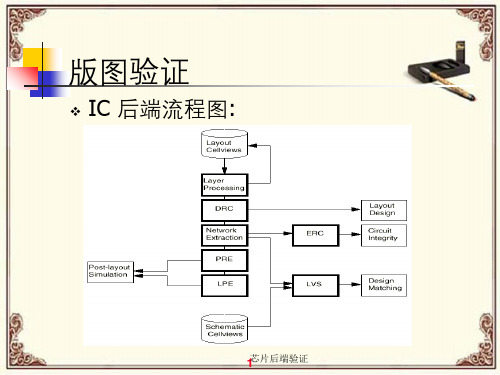

Cadence 版图设计环境的建立及设计规则的验证王翠霞,范学峰,许维胜,余有灵,王子君(同济大学半导体与信息技术研究所 上海 200092)摘 要:对版图设计需要的工艺库(techno logy file )文件、显示(disp lay )文件的书写进行了详细分析,并对设计规则验证(DRC )中遇到的问题进行了解释。
关键词:工艺库;显示文件;设计规则验证;版图中图分类号:TN 919181 文献标识码:B 文章编号:1004373X (2004)1501803Env ironm en t Setup of Layout and Ver if ica tion of D esign Rules i n CadenceW AN G Cu ix ia ,FAN Xuefeng ,XU W eisheng ,YU You ling ,W AN G Zijun(Institute of Se m iconducto r &Info r m ati on Techno l ogy ,TongjiU niversity ,Shanghai ,200092,Ch ina )Abstract :In th is paper ,the techno logy file and disp lay file w ere elabo rated exp lained befo re layou t ,and the p rob lem s of design ru le checker w ere dealed 1Keywords :techno logy file ;disp lay file ;design ru le checker ;territo ry收稿日期:20040402基金项目:AM 基金项目(0101) Cadence 提供的V irtuo so 版图设计及其验证工具强大的功能是任何其他EDA 工具所无法比拟的,故一直以来都受到了广大EDA 工程师的青睐[1],然而V irtuo so 工具的工艺库的建立和D racula 的版图验证比较繁琐。

目录目录 (1)设计环境介绍 (2)工作站常用命令 (2)运行Cadence (6)运行Layout (10)运行schematic的编辑 (15)生成schematic symbol (18)运行Artist的仿真环境 (20)设计示例的简单介绍 (21)设计环境介绍典型的全定制Full-Custom模拟集成电路设计环境1. 集成的设计环境-Cadence Design Framework II是众多Cadence 工具集成在一起的统一的界面,通过这个架构,不用繁琐的数据格式转换,就可以方便的从一个工具转到另一个工具。
其中包括很多软件,如:原理图编辑工具-Composer布局编辑工具-Candence virtuoso布局验证编辑工具-Diva, Dracula2. 电路网表或原理图编辑环境-Text editor / schematic editor3. 电路模拟软件-spice操作系统环境和硬件平台1.SUN工作站;UNIX系统2.运行Linux的PC3.作为终端的PC工作站常用命令一、在terminal窗口键入的基本命令:1. ls:列出目录下所有文件。
2. clear:清除terminal窗口里的内容。
3. pwd:显示目前工作的目录。
4. cd:改变当前目录。
5. rm:刪除文件。
6. cp:复制文件。
7. mv:移动文件。
8. mkdir:建立目录。
9. rmdir:刪除目录。
10. find:寻找文件。
11. passwd:改变当前用户密码。
12. finger:显示当前用户信息。
二、基本操作和命令的使用介绍:1.从PC登录工作站,一般使用exeed或Xmanager。
login :___________(输入username)password:___________(输入密码)2.登出步骤:点击exit3.在线命令说明(以下的example% 表示系统的提示符)example% man [command-name]4. 改变当前目录example% cd [name]Example:example% cd dir1 改变目录位置,至dir1目录下。
Tutorial: Simulating HSpice with the Analog Design Environment1.Make directory called something like cadence.$mkdir cadence2.Change to this directory.$cd cadence3.Start the Cadence Design Framework by typing “icfb &” at the command prompt.$icfb&The first window that appears is called the CIW (Command Interpreter Window).Figure 1 – CIW WindowAnother window that appears is the Library Manager. This window allows you to browse the available libraries and create your own.Figure 2 – Library Manager WindowIn the Library Manager, create a new library called EEE534. Select File->New->Library. This will open a new dialog window, in which you need to enter the name of your library, library path, and "Attach to existing tech library." Fill out the form as shown below, then select OK.Figure 3 – Create Library FormYou should see the library "EEE534" appear in the Library Manager.Figure 4 – Library Manager display newly created libraryNext, select the library you just created in the Library Manager and select File->New->Cell View.... We will create a schematic view of an inverter cell. Simply type in "INV" under cell-name and "schematic" under view. Click OK or hit the Enter key. Note: that the "Tool" is automatically set to "Composer-Schematic", the schematic editor.Figure 5 – Create New File FormAlternatively, you could select the "Composer-Schematic" tool, instead of typing out the view name. This will automatically set the view name to "schematic".After you hit "OK", the blank Composer screen will appear.Figure 6 – Virtuoso Schematic EditorTo generate a schematic, you will need to go through the following steps:•From the Schematic Window, choose Add->instance. The Component Browser, will then pop up.•In the Library field, select NCSU_Analog_Parts. We will place the pmos, nmos, vdd, gnd, vdc, vpulse andcap instances in the Schematic Window from the NCSU_Analog_Parts library asinstructed below.Note: pay special attention to the parameters specified in vdc, vpulse, and cap. These parameters are very important in simulation.Place pmos instance•In Component Browser, select P_Transistors and then pmos.•Place it in the Schematic WindowFigure 7 – Add pmos InstancePlace nmos instance•In Component Browser, select N_Transistors and then nmos.•Place it in the Schematic Window.Figure 8 – Add nmos InstancePlace gnd instance•In Component Browser, select Supply_Nets and then gnd.•Place it in the Schematic Window.Figure 9 – Add gnd Instance Place vdd instance•In Component Browser, select Supply_Nets and then vdd •Place it in the Schematic Window.Figure 10 – Add vdd InstancePlace IN pin•From the Schematic Window menu, select Add -> Pin...•In the Pin Name field , enter IN•In the Direction field, select input•Place it in the Schematic WindowFigure 11 – Add Input PinPlace OUT pin•From the Schematic Window menu, select Add -> Pin...•In the Pin Name field , enter OUT•In the Direction field, select output•Place it in the Schematic WindowFigure 12 – Add Output PinPlace vdc instance•In the Component Browser, select Voltage Sources and then vdc •In the DC voltage field, enter 5 V•Place it in the Schematic WindowFigure 13 – Add vdc SourcePlace vpulse instance•In the Component Browser, select Voltage_Sources and then vpulse •Enter the following values in the form:Figure 14 Edit Object vpulse SourcePlace cap instance•In Component Browser, select R_L_C and then cap•In the Capacitance field, enter OutCap F. (This Design Variable will be used in Artist.) •Place it in the Schematic WindowFigure 15 – Add cap InstancePlace wires•In the Schematic Window menu, select Add -> Wire (narrow)•Place wires to connect all the instances•Select Design -> Check and Save.Look at the CIW. You should see a message that says:Extracting “INV schematic”Schematic check completed with no errors.“EEE534 INV schematic” saved.If you do have some errors or warnings, the CIW will give a short explanation of what those errors are. Errors will also be marked on the schematic with a yellow or white box. Errors must be fixed for your circuit to simulate properly. When you find a warning it is up to you to decide if you shouldfix it or not. The most common warnings occur when there is a floating node or when there are wires that cross but are not connected. Just be sure that you know what effect each of these warning will have on your circuit when you simulate.Your schematic should look like the one shown below.Figure 16 – Completed SchematicIf you would like to learn more about the schematic editor, you can work through chapters 1-5 of the Composer Tutorial that comes with the Cadence documentation. Start the documentation browser by typingcdnshelp &at the command prompt. If you find that you cannot view the figures correctly in the web browser, you can click the View/Print PDF link at the top of the page to launch a PDF viewer for the tutorial. This documentation browser offers many more links for you to learn about the Cadence Design Framework.Simulate the Schematic with HSPICE within Virtuoso Analog Design EnvironmentSet up the Simulation EnvironmentYou are now prepared to simulate your circuit.From the Schematic Window menu, select Tools -> Analog Environment. A window will pop-up. This window is the Analog Design Environment Window.Figure 17 - Analog Design Environment WindowChoose a SimulatorFrom the Analog Design Environment menu, select Setup -> Simulator/Directory/Host. Enter the fields as shown below. Choose hspiceS as your simulator. Your simulation will run in the specified Project Directory. You may choose any valid pathname and filename that you like.Figure 18 Choosing Simulator/Directory/Host FormChoose AnalysisWe will setup to do a Transient Analysis on the circuit that we just produced.From the Analog Design Environment menu, select Analyses -> Choose... Fill out the form with the following values:Figure 19 – Choosing AnalysesAdd a VariableFrom the Analog Design Environment menu, select Variables -> Edit. The Editing Design Variables form will appear. Fill out the form as shown below, and then click Add to send this Variable to the Table of Design Variables.(Recall that we entered the OutCap Design Variable in the Capacitor component while editing the schematic in the previous section.)Figure 20 – Editing Design Variables FormSetup OutputWhen using Transient Analysis, the transient voltage will be saved automatically. We can save the current through capacitor C0 in the schematic by doing the following:From the Analog Design Environment menu, select Outputs -> To be Saved -> Select On Schematic In the Schematic Window, click on the lower terminal (not the wire) of capacitor C0.After you click on the terminal, the Analog Design Environment Window should look like this:Figure 21 Analog Design Environment WindownRun SimulationFrom the Analog Design Environment menu, select Simulation -> Run, Look at the echoing information in the CIW window. If the simulation succeeds, the window will display “...successful.”Figure 22 – CIW after simulationIf the simulation is unsuccessful, then one of the error messages should provide a clue as to what went wrong. Remember that you can move elements around in your schematic by clicking and dragging them. You can delete them by selecting them and pressing the “delete” key. You modify the properties of the elements by selecting them and pressing the “q” key.If you would like to learn more about the Analog Design Environment, select Analog Design Environment->Cadence Analog Design Environment User Guide in the cdnshelp browser window.View WaveformsFrom the Analog Design Environment menu, select Results -> Direct Plot -> Transient Signal. The Waveform Window will then pop up. In the Schematic Window, click on the IN wire and then Click on the OUT wire, then press ESC on your keyboard.The two curves (IN and OUT) will then be displayed in this window:Figure 23 – Waveform ViewerPress the Strip Chart Mode icon (4th icon from right) on the Waveform WindowThe waveforms will then be displayed separately as shown below:Figure 24 – Waveform Viewer, Strip Chart ModeIf you would like to learn more about the Waveform Viewer, select Analog Design Environment->Waveform User Guide in the cdnshelp browser window.Use CalculatorIn Analog Design Environment Window, go to Tools -> Calculator. The Calculator Window will then pop up, as shown below:Figure 25 – CalculatorIn Calculator Window, go to Options -> uncheck RPN. We are going to use the calculator to plot both the current through the capacitor and the absolute value of the capacitor current.In the Calculator Window, click on the tran tab then click the it radio button. In the Schematic Window, click on the lower terminal of the capacitor. Returning to the Calculator Window, the text area at the top should like this:Figure 26 – Calculator after selecting lower capacitor terminalIn the Calculator Window, press the plot icon to plot this waveform in the Waveform Window. In the Calculator Window, select the New Subwindow. In the Calculator Window, press the clear button to erase the text area, select abs, press the “(“ symbol and press the it radio button. In the Schematic Window, click on the lower terminal of the capacitor. Returning to the Calculator Window, press the “)” symbol, the text area at the top should like this:Figure 27 - Calculator after selecting lower capacitor terminalIn the Calculator Window, press the plot button to plot this waveform in the Waveform Window. Your Waveform Window should now look like this:Figure 28 – Waveform Display with current through the capacitor and the absolute value of thecapacitor current。
cadence 实验指导书哈尔滨理工大学开放性实验指导书Virtuoso Analog Design Environment中文实验手册Version 5.1.41哈尔滨理工大学开放性实验指导书实验一、熟悉Virtuoso Analog Design Environment............................................................. (2)实验二、SchematicEntry .................................................................. . (6)实验三、模拟仿真 ..................................................................... . (13)实验四、显示仿真结果 ..................................................................... .. (22)实验五、仿真结果分析 ..................................................................... .. (31)实验六、参数分析 ..................................................................... . (43)实验七、使用OCEAN 和SKILL语言(略) ................................................................. .......... 46 实验八、使用Corner分析工具 ..................................................................... . (47)实验九、Monte Carlo 分析 ..................................................................... . (50)实验十、优化分析 ..................................................................... . (59)实验十一、Component Description Format(CDF)参数 .......................................................... 64 实验十二、Macromodels、Subcircuits和InlineSubcircuits (67)实验十三、HierarchyEditor ................................................................. .. (73)实验十四、继承连接 ..................................................................... (77)哈尔滨理工大学开放性实验指导书Virtuoso Analog Design Environment 实验步骤:一、登录Linux操作系统,用安装软件的用户登录,最好不要用root用户。