掩膜板的制造讲义.
- 格式:ppt
- 大小:1.08 MB
- 文档页数:25


掩模板的制作过程在IC加⼯过程中,需要使⽤中间掩模版和光掩模版。
我们定义中间掩模版是为整个基⽚曝光⽽必须分步和重复的包含图像的⼯具。
通常图像的尺⼨被放⼤到基⽚上图像的2倍到20倍,但在⼀些情况下也⽤相等的图像。
光掩模版被定义为在⼀次曝光中能把图形转移到整个硅⽚中(或另⼀张光掩模版上)的⼯具。
中间掩模版有两种应⽤:1)把图形复印到⼯作掩模版上。
2)在分步重复对准仪中把图像直接转移到硅⽚上。
在1X硅⽚步进光刻机中,掩模版上的图形与投影到硅⽚上图形⼀样⼤;在缩⼩步进光刻机中,掩模版上的图形是放⼤的真实器件图像。
在VLSI中,电⼦束曝光10X或5X的掩模版,或直接⽤电⼦束产⽣1X 的⼯作掩模版玻璃的质量和准备:⽤以制作掩模版的玻璃必须内部和两表⾯都物缺陷。
必须于光刻胶的曝光波长下有⾼的光学透射率。
被⽤来制作掩模版的玻璃有好⼏种,包括:a)钠钙玻璃b)硼硅玻璃c)⽯英玻璃。
绿⾊的钠钙玻璃和低钠⽩钠钙玻璃(贵50%)容易被拉制成⼤⾯积的薄张,⽽且表现出很好的质量,它们热膨胀系数⾼(93×10- 7cm/cm°c),使得它门⼤⼤不适合在投影中应⽤。
在应⽤中要求低的热膨胀系数的材料,就选择硼硅玻璃和⽯英玻璃(热膨胀系数分别是37和5×10- 7cm/cm°c)。
在⼀些情况下,周围温度的变化导致硅⽚上图形的定位错误,此时就要求选择硼硅玻璃和⽯英玻璃。
⽯英圆⽚是超低膨胀系数的玻璃,它的热膨胀系数⾮常⼩。
⽯英玻璃同样在深UV和近深UV区域内有很⾼的穿透系数。
⽯英相当贵,现在倾向于发展⾼质量的合成⽯英材料。
天然⽯英通过⽕焰熔融法加⼯,⽤氧氢⽓溶化岩⽯晶体。
合成⽯英是⽤超纯SiCl4,它提供宽的光投射铝区域,低的杂质含量和少的物理缺陷。
它的应⽤随着低膨胀率和深UV的要求变得逐渐⼴泛。
圆⽚被抛光、清洗,在形成掩模图像之前被检查。
抛光是个多重步骤,在图⽚两个表⾯连续不断地分级研磨。
图⽚在检测和掩模之前被清洗、冲洗、⼲燥。

AMOLED(active-matrix organic light-emitting diode)是一种非常先进的显示技术,它能够提供更加清晰、更加色彩丰富的图像,因此在手机、电视等电子产品中得到了广泛的应用。
而在AMOLED的制造过程中,高精密金属掩膜板扮演了非常重要的角色,它可以影响到AMOLED显示屏的质量和稳定性。
为了确保AMOLED显示屏的生产工艺和质量,特编写本指导书,以帮助广大制造商正确、高效地使用高精密金属掩膜板进行AMOLED生产。
一、高精密金属掩膜板的基本概念高精密金属掩膜板是AMOLED制造过程中的重要工具,它主要用于在不同层次的AMOLED结构中进行金属材料的沉积和电镀。
高精密金属掩膜板的制备需要严格控制其表面的平整度和镀层的均匀性,以确保在生产过程中不会影响到AMOLED显示屏的图像质量。
二、高精密金属掩膜板的技术特点1. 材料选择:高精密金属掩膜板的材料需要选择高纯度的金属材料,以确保在制备过程中不会产生杂质和气泡,影响到镀层的均匀性。
2. 表面处理:高精密金属掩膜板的表面需要进行特殊处理,以提高其平整度和抗腐蚀能力,保证在生产过程中不会产生划痕和氧化。
3. 加工精度:高精密金属掩膜板的加工精度需要控制在非常小的范围内,以保证在不同层次的AMOLED结构中能够实现精准的金属沉积和电镀。
三、高精密金属掩膜板的应用注意事项1. 存储条件:高精密金属掩膜板在存储过程中需要放置在干燥、通风的环境中,以防止其表面产生水汽和污染物,影响到镀层的均匀性。
2. 清洁方法:在使用过程中需要定期对高精密金属掩膜板进行清洁,去除表面的灰尘和污渍,以保证其使用效果和寿命。
3. 操作规范:在使用高精密金属掩膜板进行AMOLED生产过程中,需要严格按照操作规程进行操作,避免在使用过程中产生损坏和变形。
四、高精密金属掩膜板的维护和保养1. 定期检测:需要定期对高精密金属掩膜板进行检测,发现问题及时进行维修和更换,以保证其使用效果和寿命。

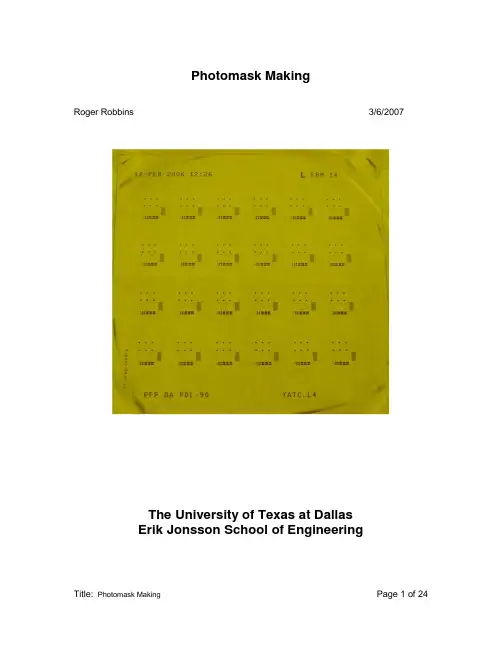
掩膜版(mask)制造技术Photomask MakingRoger Robbins 3/6/2007The University of Texas at DallasErik Jonsson School of EngineeringAuthor: Roger Robbins 3/6/2007 Document Number: SP-07-001 The University of Texas at DallasPhotomask MakingRoger Robbins 3/6/2007Table of ContentsPhotomask Making (2)Table of Contents (2)Photomask Making (3)Purpose (3)Introduction (3)Mask “Color” (3)Process Description (4)Step 1: Plasma Cleaning (4)Step 2: HMDS Application (5)Step 3: Resist Application (6)Step 5: Lithographic Patterning (8)Step 6: Post Bake (10)Step 7: Develop (10)Step 8: Plasma De-scum (11)Step 9: Cr Etch (12)Step 10: Resist Removal and Mask Clean (12)Step 11: Final Inspection (14)Conclusion (14)Appendix A (15)Appendix B (18)Title: Photomask Making Page 2 of 24 Author: Roger Robbins 3/6/2007 Document Number: SP-07-001 The University of Texas at DallasPhotomask MakingRoger Robbins 3/6/2007PurposeThis paper describes a starting process for making photomasks with the tools in the UTD Cleanroom. Special needs may dictate variations in this process flow.IntroductionPhotomasks are generally Chrome coated glass lithographic templates designed to optically transfer patterns to wafers or other substrates in order to fabricate planar type devices of all types. Basically the pattern information is created in a drawing package and stored in a database, reformatted and transferred to a lithography tool –laser writer or e-beam writer in our case – then printed in a layer of photoresist coated onto the photomask plate. The imaged pattern is next developed to form a template over the opaque Chrome and then the Chrome is etched away where the resist is clear. After the etch process is complete, the remaining photoresist is removed, the plate cleaned, and then stored for later use in an optical printer.This paper will describe in detail all the fundamental process steps required to fabricate a photomask in the UTD Cleanroom Labs.Figure 1. Example of standard photomasks: “Clear field” on left, “dark field” on rightMask “Color”First, there are some key details to discuss that determine what “color”photomask you will need to make, (Figure 1). Normally, we use “positive” photoresist to make masks. This means that wherever light exposes the photoresist, the developer willAuthor: Roger Robbins 3/6/2007 Document Number: SP-07-001 The University of Texas at Dallaswhich light will pass to expose the substrate during the pattern transfer process – (Dark Field mask color).Following that logic, if the substrate also has positive photoresist, the mask will allow exposure to the substrate in the same pattern as the clear regions on the mask. The development of the substrate resist will produce exposed areas in the same location as the clear areas on the mask. This will allow an etch process to transfer the clear area pattern to an underlying film by etching away the underlying film in the clear area.This may seem simple to the casual observer, but there is a complication when you consider the common “lift-off” process which will change the “color” of the pattern on the substrate. In the lift-off process, the patterned substrate is first developed and then a film is deposited on top of the patterned resist. The next step strips the resist under the deposited film. This will leave a pattern of deposited film in the areas where the positive photoresist was exposed and leave bare the areas under the unexposed resist that were washed away, taking the deposited film away with the wash.Then to further complicate a complicated logic, there is negative photoresist which stays put when exposed and washes away in unexposed areas. This negative process does the opposite thing to the above positive resist. The resists can be used either on the mask or the substrate in any order. Thus you must keep exact logical understanding and control of your process in order to make what you want.Process DescriptionThe following process description will assume that we start with a bare, blank photomask and describe all the steps to fabricate a complete mask. There may be sections that are optional or unnecessary due to the particular situation you have, such as a pre-coated mask that does not need to be coated with photoresist.Step 1: Plasma CleaningBoth new and recycled bare photomasks may have a thin invisible layer of organic contamination on the Cr surface. This organic layer will sometimes cause adhesion problems between the Cr and the photoresist later in the process. It also may interfere with the Cr etch process after photomask imaging. However it is easy to remove the contamination with a short, but aggressive Oxygen plasma treatment before starting the photomask process. The current process designed and tested for this purpose is shown in Table 1. It uses the March Asher1 tool, (Figure 2), but fortunately it can be used in any other month of the year as well. ?Table IMarch Asher Cleaning*Step Parameter Value1 Vacuum Pressure 230 mTorr2 Gas O23 Gas Flow 31 sccm4 Time 600 sec*Set the photomask Cr side up on the poweredelectrode plate for RIE conditions.Figure 2. March Plasma Asher tool: RF power supply at left, Control section in center,and access door to RF plasma chamber on right.Step 2: HMDS ApplicationIn order to enhance the adhesion of the photoresist to the Cr, we bake the mask in a special oven that applies a molecular monolayer of Hexamethyldisilizane (HMDS), to the surface2. This molecule chemically bonds to the Cr and then bonds to the photoresist so that the photoresist will not allow developers or etch solutions to lift the edges of resist patterns away from the mask. This step is pretty much mandatory for coating a mask prior to exposure.This is a simple process. Basically you open the oven door, insert your mask (riding on a quartz boat), close the door and push the start button. During the oven process, the mask is brought to temperature (120 C), and pressure is automatically cycled between 10 mTorr and 1200 mTorr several times to drive off moisture from the surface of the substrate. The oven fills with HMDS vapor for 5 minutes. This is the application step in which HMDS chemically attaches one end of its molecule to the substrate. The atmosphere in the oven is then cleared of vapor by introducing N2 into the oven and pumping it out again over several cycles. After about 27 minutes, the ovenspecial ? in thick Cr plated Stainless steel table normally used to level SU8 photoresist. It will take about 3 – 5 minutes to cool to room temperature.2 Daggett, Joe, Villareal, Sam, and Robbins, Roger, “UT Dallas IC Fabrication Laboratory HMDS ProcessSetup,”/doc/feb9526d3369a45177232f60ddccda38366be17c.html/research/cleanroom/documents/HMDS_Process.pdf,(2/21/2003).Title: Photomask Making Page 5 of 24 Author: Roger Robbins 3/6/2007 Document Number: SP-07-001 The University of Texas at DallasFigure 3. HMDS Oven showing logbook, mask, quartz holder with extractable handle and open door. The start button is the black button in the upper center of the control box. The red button is the reset and buzzer silencer.Step 3: Resist ApplicationAfter the blank photomask is prepared, the next step is to apply the photoresist. This is done on the CEE spinner3 manually, (Figure 4). We use two photoresists for photomasks in our lab: S1813, and AZ1518. (See Appendix A and B for resist spec sheets). Normally, the AZ1518 is pre-applied by the photomask vendor, and we don’t have to worry about applying that resist. But if we are coating a blank one, we normally use the S1813 or a new, faster resist AZ TFP650.3 Robbins, Roger “CEE Spin Coater/Hotplate Operation,”Figure 4. Manual application of S1813 photoresist to a blankphotomask in the CEE spinner.You must be trained on this tool before using. The design of the CEE spinner requires that you learn how to program the spin cycle. This is described in detail in reference #3, but verbal instruction with demonstration is required. The parameters of a nominal coating program are listed in Table 2. These parameters are regularly changed by users, so you must first check the installed values and put in your own values before coating.Table 2CEE Spinner Parameters for Mask Photoresist CoatingStep Parameter Value1 Dispense 02 Spin Speed #1 500 rpm3 Acceleration 500 rpm/sec4 Spin Time Duration #1 2 sec5 Spin Speed #2 4000 rpm6 Acceleration 4000 rpm/sec7 Spin Time Duration #2 60 seclid and starting the CEE spin cycle. For a 5 inch square photomask, the amount of photoresist is about 2 ml. The first spin cycle quickly spreads the resist without throwing it off the mask, and the second spin cycle stretches the resist film into a highly uniform thin film at the desired thickness based on a spin-speed curve from the manufacturer. For a photomask, you would typically want about 6,000 –10,000?of thickness.Title: Photomask Making Page 7 of 24 Author: Roger Robbins 3/6/2007 Document Number: SP-07-001 The University of Texas at DallasStep 4: Pre-BakeAfter the resist is coated it still contains a considerable amount of solvent that needs to be driven out via a moderately high temperature bake. This is usually done on the integral CEE spinner hotplate shown in Figure 5. This step is called “pre-bake”because it happens before exposure.Figure 5. CEE spinner hotplate with mask baking under exhaust lid.The CEE spinner has a special programmable hotplate with an integral hinged lidwith fume exhaust capabilities. This lid captures the solvent vapors emanating from thehot photoresist, and ports them away from your nose so you w on’t come down withcentral nervous system problems. Table 3 lists the baking parameters for S1813.Temperature and time are important here and vary with the photoresist type.Table 3Bake Parameters for S1813 PhotoresistStep Parameter Value1 Temperature 115 C2 Bake Time 90 secStep 5: Lithographic PatterningLithography is a complex process and will not be described here in detail. In the UTD clean room there is one method for making photomasks – the HeidelbergTitle: Photomask Making Page 8 of 24 Author: Roger Robbins 3/6/2007 Document Number: SP-07-001 The University of Texas at DallasInstruments “D WL-66” laser mask writer. The principle steps involved in making a mask are listed below.Create a device design.Lay out the mask geometries using a drawing package such as AutoCad.Convert the drawing data into a form familiar to the DWL-66 computer(.cif), using a special conversion software and special separate computer.Note: You should write a label on each mask you make to avoid using thewrong mask during your device fabrication.Send the converted data to the DWL-66 computer.Reserve time on the DWL-66 laser writerSign the LogbookLoad the resist coated photomask blank onto the laser writer stage.Set up the layout on the DWL-66 computer. Setup the job on theDWL-66 computer.Focus the DWL-66.Find the center of the photomask blank.Start the Job.Wait a long, long time before the mask is complete (many hours).Remove the mask from the DWL-66.Basically, the exposure step modifies the chemistry of the photoresist so that the exposed portion either dissolves in the developer and washes away - (Positive resist), or solidifies and remains on the mask while all the unexposed resist washes away in the developer - (Negative resist). The two photo resists listed in this document are positive resists which wash away after exposure.There are a lot of pitfalls involved with the stream of actions listed above – you must follow them exactly – deviations may cause computer confusion crashes. The lithography step will require extensive training and practice along with recurrent help –ask if you are uncertain. Use the available instruction sheets for detailed guidance so you won’t forget anything. Let us assume here that the lithography exposure goes well. Figure 6 shows the illustrious DWL-66 mask writer.Figure 6. DWL-66 Laser Mask WriterTitle: Photomask Making Page 9 of 24 Author: Roger Robbins 3/6/2007 Document Number: SP-07-001 The University of Texas at DallasStep 6: Post BakeSome resists require a short bake after exposure to “activate” the exposure. The two photomask resists, S1813 and AZ1518 do not, so we just skip right by this step in this document.Step 7: DevelopAfter exposure, the resist needs development to show the pattern. Each photoresist has its own developer and we have automatic programs set up in the CPK spin developer tools to develop your mask or wafer, (Figure 7). For optical resists, the developer chemical is basically a solution of Tetra Methyl Ammonium Hydroxide (TMAH). The rinse cycle utilizes de-ionized water.Figure 7. Photo of the CPK Spin Develop/Etch tool. The process fluids are forcedthrough the spray nozzles via pressurized source tanks (black tanks with green bolthandles in lower drawers). Note the “POLOS” controller panel at the top left of the overhead panel – this is where the tool is programmed and where process progress is displayed. Also note that if a light goes on above one of the switches at the top right, the。
掩膜版薄膜工艺
掩膜版薄膜工艺,也称为掩膜法薄膜工艺,是一种在薄膜制备过程中使用掩膜版进行模板化形状制作的方法。
以下是它的基本步骤:
1.设计模板:根据需要制作的薄膜形状,设计制作相应的掩
膜版。
掩膜版通常由透明或半透明的材料制成,如聚酯薄
膜或玻璃,上面印有所需的图案或形状。
2.准备基材:选择适当的基材进行准备。
常用的基材包括聚
合物薄膜(如聚酯薄膜、聚酰胺薄膜等)、玻璃、金属等。
3.准备薄膜涂料:根据需要制备的薄膜材料,准备相应的薄
膜涂料。
薄膜涂料可以是液态或溶液状,并根据需求可以
添加颜料或其他添加剂。
4.涂覆掩膜版:将准备好的薄膜涂料均匀涂覆在掩膜版上,
可以使用刮刀、喷涂或滚涂等方法。
确保涂料均匀、厚度
合适。
5.掩膜印刷:将涂覆有薄膜涂料的掩膜版与基材接触,轻轻
压在基材上,使薄膜涂料与基材接触并附着。
一般采用平
板印刷的方式进行掩膜印刷,也可以使用其他印刷方法。
6.固化和剥离:经过一定的固化时间,使薄膜涂料在基材上
完全固化。
然后,将掩膜版从基材上剥离,使形成的薄膜
保留在基材上。
7.后处理:根据需要,可以对薄膜进行后处理,如烘干、硬
化、清洗等,以进一步改善薄膜品质和性能。
掩膜版薄膜工艺适用于许多应用,如柔性显示器、光学薄膜、微电子器件等领域。
它允许制备出具有特定形状和性能的薄膜,具有一定的灵活性和可塑性。

Photomask MakingRoger Robbins 3/6/2007The University of Texas at DallasErik Jonsson School of EngineeringTitle: Photomask Making Page 1 of 24Author: Roger Robbins 3/6/2007 Document Number: SP-07-001 The University of Texas at DallasPhotomask MakingRoger Robbins 3/6/2007Table of ContentsPhotomask Making (2)Table of Contents (2)Photomask Making (3)Purpose (3)Introduction (3)Mask “Color” (3)Process Description (4)Step 1: Plasma Cleaning (4)Step 2: HMDS Application (5)Step 3: Resist Application (6)Step 4: Pre-Bake (8)Step 5: Lithographic Patterning (8)Step 6: Post Bake (10)Step 7: Develop (10)Step 8: Plasma De-scum (11)Step 9: Cr Etch (12)Step 10: Resist Removal and Mask Clean (12)Step 11: Final Inspection (14)Conclusion (14)Appendix A (15)Appendix B (18)Title: Photomask Making Page 2 of 24 Author: Roger Robbins 3/6/2007 Document Number: SP-07-001 The University of Texas at DallasPhotomask MakingRoger Robbins 3/6/2007PurposeThis paper describes a starting process for making photomasks with the tools in the UTD Cleanroom. Special needs may dictate variations in this process flow.IntroductionPhotomasks are generally Chrome coated glass lithographic templates designed to optically transfer patterns to wafers or other substrates in order to fabricate planar type devices of all types. Basically the pattern information is created in a drawing package and stored in a database, reformatted and transferred to a lithography tool –laser writer or e-beam writer in our case – then printed in a layer of photoresist coated onto the photomask plate. The imaged pattern is next developed to form a template over the opaque Chrome and then the Chrome is etched away where the resist is clear. After the etch process is complete, the remaining photoresist is removed, the plate cleaned, and then stored for later use in an optical printer.This paper will describe in detail all the fundamental process steps required to fabricate a photomask in the UTD Cleanroom Labs.Figure 1. Example of standard photomasks: “Clear field” on left, “dark field” on rightMask “Color”First, there are some key details to discuss that determine what “color”photomask you will need to make, (Figure 1). Normally, we use “positive” photoresist to make masks. This means that wherever light exposes the photoresist, the developer will wash away the photoresist. This exposed area, then, will expose the Chrome and allow it to be washed away in the acid etch solution, leaving holes in the Chrome throughTitle: Photomask Making Page 3 of 24Author: Roger Robbins 3/6/2007 Document Number: SP-07-001 The University of Texas at Dallaswhich light will pass to expose the substrate during the pattern transfer process – (Dark Field mask color).Following that logic, if the substrate also has positive photoresist, the mask will allow exposure to the substrate in the same pattern as the clear regions on the mask. The development of the substrate resist will produce exposed areas in the same location as the clear areas on the mask. This will allow an etch process to transfer the clear area pattern to an underlying film by etching away the underlying film in the clear area.This may seem simple to the casual observer, but there is a complication when you consider the common “lift-off” process which will change the “color” of the pattern on the substrate. In the lift-off process, the patterned substrate is first developed and then a film is deposited on top of the patterned resist. The next step strips the resist under the deposited film. This will leave a pattern of deposited film in the areas where the positive photoresist was exposed and leave bare the areas under the unexposed resist that were washed away, taking the deposited film away with the wash.Then to further complicate a complicated logic, there is negative photoresist which stays put when exposed and washes away in unexposed areas. This negative process does the opposite thing to the above positive resist. The resists can be used either on the mask or the substrate in any order. Thus you must keep exact logical understanding and control of your process in order to make what you want.Process DescriptionThe following process description will assume that we start with a bare, blank photomask and describe all the steps to fabricate a complete mask. There may be sections that are optional or unnecessary due to the particular situation you have, such as a pre-coated mask that does not need to be coated with photoresist.Step 1: Plasma CleaningBoth new and recycled bare photomasks may have a thin invisible layer of organic contamination on the Cr surface. This organic layer will sometimes cause adhesion problems between the Cr and the photoresist later in the process. It also may interfere with the Cr etch process after photomask imaging. However it is easy to remove the contamination with a short, but aggressive Oxygen plasma treatment before starting the photomask process. The current process designed and tested for this purpose is shown in Table 1. It uses the March Asher1 tool, (Figure 2), but fortunately it can be used in any other month of the year as well. ☺Table IMarch Asher Cleaning*Step Parameter Value1 Vacuum Pressure 230 mTorr2 Gas O23 Gas Flow 31 sccm4 Time 600 sec1 Roger Robbins, “March Asher Operation,”/~rar011300/public_html/MarchAsher/MarchAsherOperation.pdf,(7/31/2006)Title: Photomask Making Page 4 of 24 Author: Roger Robbins 3/6/2007 Document Number: SP-07-001 The University of Texas at Dallas*Set the photomask Cr side up on the poweredelectrode plate for RIE conditions.Figure 2. March Plasma Asher tool: RF power supply at left, Control section in center,and access door to RF plasma chamber on right.Step 2: HMDS ApplicationIn order to enhance the adhesion of the photoresist to the Cr, we bake the mask in a special oven that applies a molecular monolayer of Hexamethyldisilizane (HMDS), to the surface2. This molecule chemically bonds to the Cr and then bonds to the photoresist so that the photoresist will not allow developers or etch solutions to lift the edges of resist patterns away from the mask. This step is pretty much mandatory for coating a mask prior to exposure.This is a simple process. Basically you open the oven door, insert your mask (riding on a quartz boat), close the door and push the start button. During the oven process, the mask is brought to temperature (120 C), and pressure is automatically cycled between 10 mTorr and 1200 mTorr several times to drive off moisture from the surface of the substrate. The oven fills with HMDS vapor for 5 minutes. This is the application step in which HMDS chemically attaches one end of its molecule to the substrate. The atmosphere in the oven is then cleared of vapor by introducing N2 into the oven and pumping it out again over several cycles. After about 27 minutes, the oven buzzes rather loudly indicating it is done. Reset the buzzer, open the oven door and remove your mask using the forked lifting tool – the mask is hotter than boiling water (120 C). Let it cool. Cooling is important because the temperature uniformity of the mask determines the film thickness uniformity during the spin coating of the resist. To quickly achieve temperature uniformity, set the mask on a cool metal surface like thespecial ½ in thick Cr plated Stainless steel table normally used to level SU8 photoresist. It will take about 3 – 5 minutes to cool to room temperature.2 Daggett, Joe, Villareal, Sam, and Robbins, Roger, “UT Dallas IC Fabrication Laboratory HMDS Process Setup,”/research/cleanroom/documents/HMDS_Process.pdf,(2/21/2003).Title: Photomask Making Page 5 of 24 Author: Roger Robbins 3/6/2007 Document Number: SP-07-001 The University of Texas at DallasFigure 3. HMDS Oven showing logbook, mask, quartz holder with extractable handle and open door. The start button is the black button in the upper center of the control box. The red button is the reset and buzzer silencer.Step 3: Resist ApplicationAfter the blank photomask is prepared, the next step is to apply the photoresist. This is done on the CEE spinner3 manually, (Figure 4). We use two photoresists for photomasks in our lab: S1813, and AZ1518. (See Appendix A and B for resist spec sheets). Normally, the AZ1518 is pre-applied by the photomask vendor, and we don’t have to worry about applying that resist. But if we are coating a blank one, we normally use the S1813 or a new, faster resist AZ TFP650.3 Robbins, Roger “CEE Spin Coater/Hotplate Operation,”/research/cleanroom/documents/CEEcoater.pdf, (10/7/2004).Title: Photomask MakingPage 6 of 24Author: Roger Robbins 3/6/2007 Document Number: SP-07-001 The University of Texas at DallasFigure 4. Manual application of S1813 photoresist to a blankphotomask in the CEE spinner.You must be trained on this tool before using. The design of the CEE spinner requires that you learn how to program the spin cycle. This is described in detail in reference #3, but verbal instruction with demonstration is required. The parameters of a nominal coating program are listed in Table 2. These parameters are regularly changed by users, so you must first check the installed values and put in your own values before coating.Table 2CEE Spinner Parameters for Mask Photoresist CoatingStep Parameter Value1 Dispense 02 Spin Speed #1 500 rpm3 Acceleration 500 rpm/sec4 Spin Time Duration #1 2 sec5 Spin Speed #2 4000 rpm6 Acceleration 4000 rpm/sec7 Spin Time Duration #2 60 secThe resist is dispensed from a plastic pipette by sucking up just the right amount of liquid photoresist and dispensing it onto the center of the wafer and then closing thelid and starting the CEE spin cycle. For a 5 inch square photomask, the amount of photoresist is about 2 ml. The first spin cycle quickly spreads the resist without throwing it off the mask, and the second spin cycle stretches the resist film into a highly uniform thin film at the desired thickness based on a spin-speed curve from the manufacturer. For a photomask, you would typically want about 6,000 –10,000Ǻof thickness.Title: Photomask Making Page 7 of 24 Author: Roger Robbins 3/6/2007 Document Number: SP-07-001 The University of Texas at DallasStep 4: Pre-BakeAfter the resist is coated it still contains a considerable amount of solvent that needs to be driven out via a moderately high temperature bake. This is usually done on the integral CEE spinner hotplate shown in Figure 5. This step is called “pre-bake”because it happens before exposure.Figure 5. CEE spinner hotplate with mask baking under exhaust lid.The CEE spinner has a special programmable hotplate with an integral hinged lidwith fume exhaust capabilities. This lid captures the solvent vapors emanating from thehot photoresist, and ports them away from your nose so you w on’t come down withcentral nervous system problems. Table 3 lists the baking parameters for S1813.Temperature and time are important here and vary with the photoresist type.Table 3Bake Parameters for S1813 PhotoresistStep Parameter Value1 Temperature 115 C2 Bake Time 90 secStep 5: Lithographic PatterningLithography is a complex process and will not be described here in detail. In the UTD clean room there is one method for making photomasks – the HeidelbergTitle: Photomask Making Page 8 of 24 Author: Roger Robbins 3/6/2007 Document Number: SP-07-001 The University of Texas at DallasInstruments “D WL-66” laser mask writer. The principle steps involved in making a mask are listed below.Create a device design.Lay out the mask geometries using a drawing package such as AutoCad.Convert the drawing data into a form familiar to the DWL-66 computer(.cif), using a special conversion software and special separate computer.Note: You should write a label on each mask you make to avoid using thewrong mask during your device fabrication.Send the converted data to the DWL-66 computer.Reserve time on the DWL-66 laser writerSign the LogbookLoad the resist coated photomask blank onto the laser writer stage.Set up the layout on the DWL-66 computer. Setup the job on theDWL-66 computer.Focus the DWL-66.Find the center of the photomask blank.Start the Job.Wait a long, long time before the mask is complete (many hours).Remove the mask from the DWL-66.Basically, the exposure step modifies the chemistry of the photoresist so that the exposed portion either dissolves in the developer and washes away - (Positive resist), or solidifies and remains on the mask while all the unexposed resist washes away in the developer - (Negative resist). The two photo resists listed in this document are positive resists which wash away after exposure.There are a lot of pitfalls involved with the stream of actions listed above – you must follow them exactly – deviations may cause computer confusion crashes. The lithography step will require extensive training and practice along with recurrent help –ask if you are uncertain. Use the available instruction sheets for detailed guidance so you won’t forget anything. Let us assume here that the lithography exposure goes well. Figure 6 shows the illustrious DWL-66 mask writer.Figure 6. DWL-66 Laser Mask WriterTitle: Photomask Making Page 9 of 24 Author: Roger Robbins 3/6/2007 Document Number: SP-07-001 The University of Texas at DallasStep 6: Post BakeSome resists require a short bake after exposure to “activate” the exposure. The two photomask resists, S1813 and AZ1518 do not, so we just skip right by this step in this document.Step 7: DevelopAfter exposure, the resist needs development to show the pattern. Each photoresist has its own developer and we have automatic programs set up in the CPK spin developer tools to develop your mask or wafer, (Figure 7). For optical resists, the developer chemical is basically a solution of Tetra Methyl Ammonium Hydroxide (TMAH). The rinse cycle utilizes de-ionized water.Figure 7. Photo of the CPK Spin Develop/Etch tool. The process fluids are forcedthrough the spray nozzles via pressurized source tanks (black tanks with green bolthandles in lower drawers). Note the “POLOS” controller panel at the top left of the overhead panel – this is where the tool is programmed and where process progress is displayed. Also note that if a light goes on above one of the switches at the top right, the fluid is low in that particular pressure canister. It will complete the current process evenif the light goes on during process.The steps involved in developing the mask in the CPK acid/base developer tool are as follows:Sign the LOGBOOKInsure that the machine is on – press the green start button on theoverhead panel if needed.When the display asks for help, follow the directions on screen and pressthe “other” button – (the blank pad between the “MODE” and “UP arrow”).If required, exchange the substrate holder for the appropriate sized maskholder. This involves turning off the “VACUUM” on the controller paneland lifting the chuck off the spindle, then replacing it with the appropriatemask holder. Note that the fit between holder and spindle is tight andrequires that the two posts on the spindle fit into the receiver holes on the Title: Photomask Making Page 10 of 24 Author: Roger Robbins 3/6/2007 Document Number: SP-07-001 The University of Texas at Dallasbottom of the chuck assembly. Place the chuck over the spindle andslide it around until the two posts slip into the receiver holes and thechuck base seats against the o-ring in the spindle.Turn on the vacuum by pressing the “VAC” button on the overhead panelcontroller. Check to see that the chuck is properly seated and will notwobble excessively during the rotation.Place the mask securely inside the corner posts on the substrate holder.Close the lid.Select the proper program number from the list of programs posted justunder the controller on the overhead panel. Enter this program numberby pressing the “PROGRAM” button, entering the appropriate number, (2for S1813), then pressing the “ENTER” button.To start the develop program, press the I/O button at the lower left of theoverhead display.The develop program has a multitude of steps and comes to a completestop several times to “puddle-develop” in order to save developer fluid.Allow the program to complete and then press “VAC” to open the lid andremove your developed mask. NOTE: These lids are notorious fordripping fluid droplets on perfectly good masks – be very gentle in liftingthe lid.Close the lid and remove your mask.Step 8: Plasma De-scumAfter development, have a look at your pattern under a microscope. Look at it for a long time to check the pattern and quality of develop. Look for things like scalloped resist edges, lifted resist, pinholes, under or over development, particles, and other things that look like they could damage the image. If a severe fault is found, do not go on to the next step. Stop and recycle the mask. The resist can be stripped off and new resist applied at this point, saving cost and material.If the inspection goes well, you need to prepare for the Cr etch. The first thing to do here is to insure that all of the pattern will etch in the etch time allowed. This can be helped if you do a very light O2 “de-scum” etch in the March Asher. The “de-scum” etch parameters are listed in Table 4.Table 4March Etcher “Descum” ParametersParameter Value1 Gas O22 Flow of gas313 RF Power50 Watts4 Etch Time10 secThe effect of this light etch is to clean out the bottom of the developed features in the resist. This insures that there are no areas covered with a very thin film of resist leftby the developer. If all is clean, the etch process will be uniform and complete all at once.Title: Photomask Making Page 11 of 24 Author: Roger Robbins 3/6/2007 Document Number: SP-07-001 The University of Texas at DallasStep 9: Cr EtchAfter the short plasma “de-scum,” it is time to do the Cr etch. This etch can be accomplished on the CPK developer/etcher that developed the mask in the first place. Just select the Cr etch program and set the mask firmly into the corner post nests. The actual operation is very similar to the CPK develop program in Step 7, and the steps are outlined below.Sign the LOGBOOKInsure that the machine is on – press the green start button on theoverhead panel if necessary.When the display asks for help, follow the directions on screen and pressthe “other” button – (the blank pad between the “MODE” and “UP arrow”).If required, exchange the substrate holder for the appropriate sized maskholder. This involves turning off the “VACUUM” on the controller paneland lifting the chuck off the spindle, then replacing it with the appropriatemask holder. Note that the fit between holder and spindle is tight andrequires that the two posts on the spindle fit into the receiver holes on thebottom of the chuck assembly. Place the chuck over the spindle andslide it around until the two posts slip into the receiver holes and thechuck base seats against the o-ring in the spindle.Turn on the vacuum by pressing the “VAC” button on the overhead panelcontroller. Check to see that the chuck is properly seated and will notwobble excessively during the rotation.Place the mask securely inside the corner posts on the substrate holder.Close the lid.Select the proper program number from the list of programs posted justunder the controller on the overhead panel. Enter this program numberby pressing the “PROGRAM” button, entering the appropriate number, (4for Cr Etch), and hitting the “ENTER” button.To start the etch program, press the I/O button at the lower left of theoverhead display.The etch program has a multitude of steps and comes to a complete stopseveral times to “Puddle” develop in order to save etch fluid.Allow the program to complete and then press “VAC” to open the lid andremove your etched mask. NOTE: These lids are notorious for drippingdroplets on perfectly good masks, so be very gentle in lifting the lid.Close the lid.Step 10: Resist Removal and Mask CleanAfter inspecting the etched pattern under a microscope, it is time to remove the photoresist from the mask. This is done to avoid polymer-to-polymer contact at the contact print step between the old resist on the mask and the new coat of resist on a wafer. Polymer contact generates high friction and the resist on the wafer could be torn by sliding the wafer around during alignment.This resist removal can usually be done in the solvent CPK spinner. This tool is very similar to the CPK Chrome etch spinner – identical control and user interface, so Title: Photomask Making Page 12 of 24Author: Roger Robbins 3/6/2007 Document Number: SP-07-001 The University of Texas at Dallasthe instructions are almost identical to the previous section – simply select the Acetone Strip program and run your mask. This process uses puddles of Acetone to dissolve the photoresist remaining on the photomask and then spins it off and finally rinses the mask with Isopropyl Alcohol.To assure that the photoresist film is chemically removed, you can also send the mask through the March Asher using the same procedure as described in Step 1: “Plasma Cleaning.”Mask CleaningAs a final cleanup to remove remnants from the CPK process, particularly from the back side, you can clean the mask in the UltraTech Mask Washer. Use program “0”for a simple high pressure DI water wash of both sides. This tool is pictured in Figure 8 with its control panel.Note that the big rotor has to be balanced before starting the wash. When you load your mask onto the spin wheel, another mask of the exact mass as yours has to be loaded opposite to yours or the resulting momentum vibration during the spin cycle will cause the tool to stop to protect itself and your mask from disaster. Make sure the balancing mask is the same mass as your mask – compare the thickness! The Door to the chamber opens by sliding downwards after you release the latch with the black button at the lower left of the control panel (below and left of the “Big Red emergency OFF” button).To select the program to run, press “Go To Program,” then “0,” and then “Enter”to access the water-only wash program “0.”This will load the “0” program and indicate it by placing a “0” in the “Prog” box in the upper right of the keypad area. To start the program, press the “Off/On Start” button in the upper left of the instruction keypad.Figure 8. UltraTech Mask Washer.Title: Photomask Making Page 13 of 24Author: Roger Robbins 3/6/2007 Document Number: SP-07-001 The University of Texas at DallasStep 11: Final InspectionThe last step should be a thorough inspection of the etched pattern. It is better to find errors and poor quality at this stage than after a bad pattern that can potentially ruin a multi-level substrate.ConclusionThis document has briefly illustrated the Masking making lithography trail through the UTD Clean Room Labs. Once the mask is made, a new trail is followed to transfer the mask pattern to a substrate to build a device. That trail is multivariate and depends on the device being fabricated. Usually, instruction for that portion of the trail is obtained from your research group or directly from literature. Cleanroom staff can help with additional advice if necessary. Take care and be SAFE!Title: Photomask Making Page 14 of 24Author: Roger Robbins 3/6/2007 Document Number: SP-07-001 The University of Texas at DallasAppendix AS1813 Photoresist Spec SheetRather than clutter up this document with an appendix of many pages, please find the data on the web. The spec sheet for S1813 photoresist can be found on the web at the following address: http://cmi.epfl.ch/materials/Data_S1800.pdf Well, I suppose I should include the spin speed curves and the dose characteristic since I had to include the data sheet for the other resist.Title: Photomask Making Page 15 of 24 Author: Roger Robbins 3/6/2007 Document Number: SP-07-001 The University of Texas at DallasAppendix BAZ1518 Photoresist Spec SheetIt seems that the manufacturer of AZ1518 does not post its data sheets on the internet. Consequently, I will clutter up this document with a copied version of their data sheet.Author: Roger Robbins 3/6/2007 Document Number: SP-07-001 The University of Texas at Dallas。

掩膜板玻璃基板工艺流程那咱们就开始聊聊掩膜板玻璃基板的工艺流程吧。
一、玻璃基板的准备。
二、镀膜工序。
镀膜就像是给玻璃基板穿上一层漂亮的衣服。
这层膜可不是随随便便就能镀上去的呢。
要用到特殊的设备和材料。
比如说,有的镀膜材料像那种特别珍贵的调料一样,得小心翼翼地用。
在镀膜的时候呀,设备得调整到刚刚好的状态,温度啦、压力啦,这些都很关键。
就像我们煮菜,火候和调料的比例不对,菜就不好吃。
这个膜的厚度也得均匀,要是有的地方厚有的地方薄,那就像我们穿的衣服,这里一块补丁那里一块薄的,多难看呀。
而且这个镀膜过程中得一直监控着,就像照顾小婴儿一样,一刻都不能放松,得随时看看有没有什么异常情况。
三、光刻工序。
光刻这一步就像是在玻璃基板上画画一样。
不过这个画画可不容易,是要用很精密的仪器来操作的。
首先得有个设计好的图案,这个图案就像我们画画的草图一样重要。
然后把这个图案通过光刻设备转移到玻璃基板上。
这时候呀,设备的精度就特别重要啦。
就像我们刺绣,一针绣歪了,整个图案可能就毁了。
而且光刻的时候对环境的要求也很高,得在那种很干净、很稳定的环境里进行,就像我们做艺术品,周围环境乱糟糟的,肯定做不好呀。
在光刻过程中,还得时不时地检查一下刻出来的图案是不是符合要求,要是不符合,就得赶紧调整,可不能将错就错哦。
四、蚀刻工序。
蚀刻就像是把光刻出来的图案进一步加工,让它更清晰、更准确。
这个蚀刻液就像一把神奇的雕刻刀。
但是这把雕刻刀可不好控制呢。
蚀刻液的浓度要合适,太浓了可能就把不该刻掉的地方也刻掉了,太稀了又刻不动。
就像我们刷牙用的牙膏,太多了浪费还容易起泡泡到处都是,太少了又刷不干净。
在蚀刻的时候,也要注意时间,时间太长或者太短都不行。
而且蚀刻完了之后,还得把玻璃基板清洗得干干净净的,不能有蚀刻液残留,不然就像吃完饭不擦嘴一样,多不卫生呀。
五、检查与包装。
掩膜板玻璃基板的工艺流程每一步都很重要,就像我们身体的各个器官一样,少了哪个都不行。