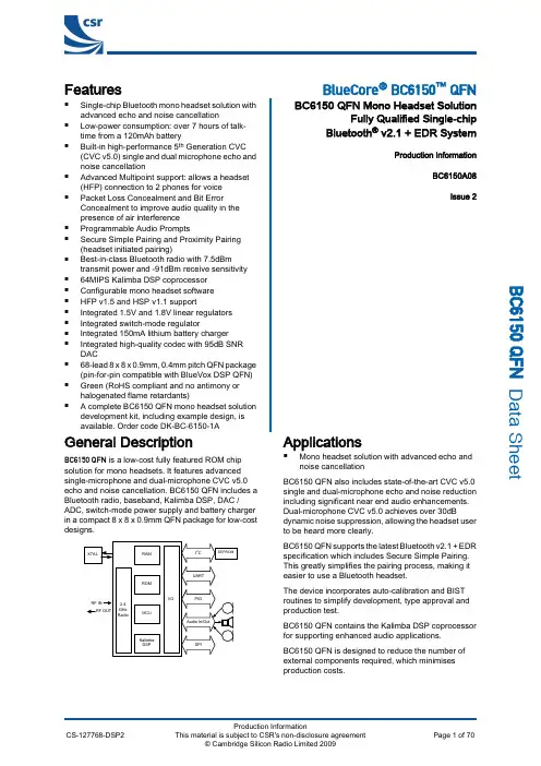
Features _äìÉ`çêÉ∆=_`SNRM »=nck■Single-chip Bluetooth mono headset solution withadvanced echo and noise cancellation ■Low-power consumption: over 7 hours of talk-time from a 120mAh battery ■Built-in high-performance 5th Generation CVC(CVC v5.0) single and dual microphone echo and noise cancellation■Advanced Multipoint support: allows a headset (HFP) connection to 2 phones for voice■Packet Loss Concealment and Bit Error Concealment to improve audio quality in thepresence of air interference■Programmable Audio Prompts■Secure Simple Pairing and Proximity Pairing(headset initiated pairing)■Best-in-class Bluetooth radio with 7.5dBmtransmit power and -91dBm receive sensitivity■64MIPS Kalimba DSP coprocessor■Configurable mono headset software■HFP v1.5 and HSP v1.1 support■Integrated 1.5V and 1.8V linear regulators■Integrated switch-mode regulator■Integrated 150mA lithium battery charger■Integrated high-quality codec with 95dB SNRDAC■68-lead 8 x 8 x 0.9mm, 0.4mm pitch QFN package(pin-for-pin compatible with BlueVox DSP QFN)■Green (RoHS compliant and no antimony orhalogenated flame retardants)■ A complete BC6150 QFN mono headset solutiondevelopment kit, including example design, isavailable. Order code DK‑BC‑6150‑1ABC6150 QFN Mono Headset SolutionFully Qualified Single-chipBluetooth ® v2.1 + EDR SystemProduction InformationBC6150A08Issue 2General Description _`SNRM=nck is a low-cost fully featured ROM chip solution for mono headsets. It features advanced single-microphone and dual-microphone CVC v5.0echo and noise cancellation. BC6150 QFN includes a Bluetooth radio, baseband, Kalimba DSP, DAC /ADC, switch-mode power supply and battery charger in a compact 8 x 8 x 0.9mm QFN package for low-cost designs.Applications■Mono headset solution with advanced echo andnoise cancellationBC6150 QFN also includes state-of-the-art CVC v5.0single and dual-microphone echo and noise reductionincluding significant near end audio enhancements.Dual-microphone CVC v5.0 achieves over 30dBdynamic noise suppression, allowing the headset userto be heard more clearly.BC6150 QFN supports the latest Bluetooth v2.1 + EDRspecification which includes Secure Simple Pairing.This greatly simplifies the pairing process, making iteasier to use a Bluetooth headset.The device incorporates auto-calibration and BISTroutines to simplify development, type approval andproduction test.BC6150 QFN contains the Kalimba DSP coprocessorfor supporting enhanced audio applications.BC6150 QFN is designed to reduce the number ofexternal components required, which minimisesproduction costs._`SNRM=nck Data SheetDocument History RevisionDate Change Reason127 AUG 09Original publication of this document.213 NOV 09Production Information added.SPI interface information updated.If you have any comments about this document, email comments@ givingthe number, title and section with your feedback.Document History_`SNRM=nck Data SheetStatus InformationThe status of this Data Sheet is Production Information .CSR Product Data Sheets progress according to the following format:Advance InformationInformation for designers concerning CSR product in development. All values specified are the target values of thedesign. Minimum and maximum values specified are only given as guidance to the final specification limits and mustnot be considered as the final values.All detailed specifications including pinouts and electrical specifications may be changed by CSR without notice.Pre-production InformationPinout and mechanical dimension specifications finalised. All values specified are the target values of the design.Minimum and maximum values specified are only given as guidance to the final specification limits and must not beconsidered as the final values.All electrical specifications may be changed by CSR without notice.Production InformationFinal Data Sheet including the guaranteed minimum and maximum limits for the electrical specifications.Production Data Sheets supersede all previous document versions.Life Support Policy and Use in Safety-critical ApplicationsCSR's products are not authorised for use in life-support or safety-critical applications. Use in such applications isdone at the sole discretion of the customer. CSR will not warrant the use of its devices in such applications.CSR Green Semiconductor Products and RoHS ComplianceBC6150 QFN devices meet the requirements of Directive 2002/95/EC of the European Parliament and of the Councilon the Restriction of Hazardous Substance (RoHS).BC6150 QFN devices are also free from halogenated or antimony trioxide-based flame retardants and otherhazardous chemicals. For more information, see CSR's Environmental Compliance Statement for CSR GreenSemiconductor Products .Trademarks, Patents and LicencesUnless otherwise stated, words and logos marked with ™ or ® are trademarks registered or owned by CSR plc or itsaffiliates. Bluetooth ® and the Bluetooth ® logos are trademarks owned by Bluetooth ® SIG, Inc. and licensed toCSR. Other products, services and names used in this document may have been trademarked by their respectiveowners.The publication of this information does not imply that any license is granted under any patent or other rights ownedby CSR plc and/or its affiliates.CSR reserves the right to make technical changes to its products as part of its development programme.While every care has been taken to ensure the accuracy of the contents of this document, CSR cannot acceptresponsibility for any errors.Refer to for compliance and conformance to standards information.Status Information_`SNRM=nck Data SheetContents1Device Details (8)2Functional Block Diagram (9)3Package Information (10)3.1Pinout Diagram (10)3.2Device Terminal Functions (11)3.3Package Dimensions (15)3.4PCB Design and Assembly Considerations (16)3.5Typical Solder Reflow Profile (16)4Bluetooth Modem (17)4.1RF Ports (17)4.1.1RF_N and RF_P (17)4.2RF Receiver (17)4.2.1Low Noise Amplifier (17)4.2.2RSSI Analogue to Digital Converter (17)4.3RF Transmitter (18)4.3.1IQ Modulator (18)4.3.2Power Amplifier (18)4.4Bluetooth Radio Synthesiser (18)4.5Baseband (18)4.5.1Burst Mode Controller (18)4.5.2Physical Layer Hardware Engine (18)4.6Basic Rate Modem (18)4.7Enhanced Data Rate Modem (18)5Clock Generation (20)5.1Clock Architecture (20)5.2Input Frequencies and PS Key Settings (20)5.3External Reference Clock (20)5.3.1Input: XTAL_IN (20)5.3.2XTAL_IN Impedance in External Mode (21)5.3.3Clock Start-up Delay (21)5.3.4Clock Timing Accuracy (21)5.4Crystal Oscillator: XTAL_IN and XTAL_OUT (22)5.4.1Load Capacitance (23)5.4.2Frequency Trim (23)5.4.3Transconductance Driver Model (24)5.4.4Negative Resistance Model (24)5.4.5Crystal PS Key Settings (25)6Bluetooth Stack Microcontroller (26)6.1Programmable I/O Ports, PIO and AIO (26)7Kalimba DSP (27)8Memory Interface and Management (28)8.1Memory Management Unit (28)8.2System RAM (28)8.3Kalimba DSP RAM (28)8.4Internal ROM (28)9Serial Interfaces (29)9.1UART Interface (29)9.1.1UART Configuration While Reset is Active (31)9.2Programming and Debug Interface (31)9.2.1Instruction Cycle ..................................................................................................................... 31_`SNRM=nck Data Sheet9.2.2Multi-slave Operation (31)9.3I 2C Interface (31)10Audio Interface (33)10.1Audio Input and Output (33)10.2Mono Audio Codec Interface (33)10.2.1Mono Audio Codec Block Diagram (34)10.2.2ADC (34)10.2.3ADC Digital Gain (34)10.2.4ADC Analogue Gain (35)10.2.5DAC (35)10.2.6DAC Digital Gain (35)10.2.7DAC Analogue Gain (36)10.2.8Microphone Input (36)10.2.9Output Stage (39)10.2.10Side Tone (40)10.2.11Integrated Digital Filter (40)11Power Control and Regulation (42)11.1Power Sequencing (42)11.2External Voltage Source (42)11.3Switch-mode Regulator (43)11.4Low-voltage Linear Regulator (43)11.5Low-voltage Audio Linear Regulator (43)11.6Voltage Regulator Enable Pins (44)11.7Battery Charger (44)11.8LED Drivers (44)11.9Reset, RST# (45)11.9.1Digital Pin States on Reset (46)11.9.2Status after Reset (46)12Example Application Schematic (47)13Electrical Characteristics (48)13.1ESD Precautions (48)13.2Absolute Maximum Ratings (48)13.3Recommended Operating Conditions (48)13.4Input/Output Terminal Characteristics (49)13.4.1Low-voltage Linear Regulator (49)13.4.2Low-voltage Linear Audio Regulator (50)13.4.3Switch-mode Regulator (51)13.4.4Battery Charger (52)13.4.5Reset (53)13.4.6Regulator Enable (53)13.4.7Digital Terminals (54)13.4.8Mono Codec: Analogue to Digital Converter (55)13.4.9Mono Codec: Digital to Analogue Converter (56)13.4.10Clocks (57)13.4.11LED Driver Pads (57)13.4.12Auxiliary ADC (58)14Power Consumption (59)15CSR Green Semiconductor Products and RoHS Compliance (61)15.1RoHS Statement (61)15.1.1List of Restricted Materials (61)16BC6150 QFN Software Stack (62)16.1BC6150 QFN Mono Headset Solution Development Kit (62)16.2BC6150 QFN Mono Headset Solution ................................................................................................. 62_`SNRM=nck Data Sheet16.3Advanced Multipoint Support (62)16.4Programmable Audio Prompts (63)16.5Proximity Pairing (63)16.5.1Proximity Pairing Configuration (63)17Ordering Information (64)17.1BC6150 QFN Mono Headset Solution Development Kit Ordering Information (64)18Tape and Reel Information (65)18.1Tape Orientation (65)18.2Tape Dimensions (65)18.3Reel Information (66)18.4Moisture Sensitivity Level (66)19Document References (67)Terms and Definitions (68)List of FiguresFigure 2.1Functional Block Diagram (9)Figure 3.1Device Pinout (10)Figure 3.2Package Dimensions (15)Figure 4.1Simplified Circuit RF_N and RF_P (17)Figure 4.2BDR and EDR Packet Structure (19)Figure 5.1Clock Architecture (20)Figure 5.2TCXO Clock Accuracy (22)Figure 5.3Crystal Driver Circuit (22)Figure 5.4Crystal Equivalent Circuit (23)Figure 7.1Kalimba DSP Interface to Internal Functions (27)Figure 9.1Universal Asynchronous Receiver (29)Figure 9.2Break Signal (30)Figure 9.3Example EEPROM Connection (32)Figure 10.1BC6150 QFN Audio Interface (33)Figure 10.2Mono Codec Audio Input and Output Stages (34)Figure 10.3ADC Analogue Amplifier Block Diagram (35)Figure 10.4Microphone Biasing (36)Figure 10.5Speaker Output (40)Figure 11.1Voltage Regulator Configuration (42)Figure 11.2LED Equivalent Circuit (45)Figure 12.1Example Application Schematic (47)Figure 16.1Programmable Audio Prompts in External I 2C EEPROM (63)Figure 18.1BC6150 QFN Tape Orientation (65)Figure 18.2Reel Dimensions (66)List of TablesTable 4.1Data Rate Schemes (19)Table 5.1External Clock Specifications (21)Table 5.2Crystal Specification (23)Table 9.1Possible UART Settings (29)Table 9.2Standard Baud Rates (30)Table 9.3Instruction Cycle for a SPI Transaction (31)Table 10.1ADC Digital Gain Rate Selection (34)Table 10.2DAC Digital Gain Rate Selection (35)Table 10.3DAC Analogue Gain Rate Selection (36)Table 10.4Voltage Output Steps ....................................................................................................................... 38_`SNRM=nck Data SheetTable 10.5Current Output Steps (39)Table 11.1BC6150 QFN Voltage Regulator Enable Pins (44)Table 11.2BC6150 QFN Digital Pin States on Reset (46)List of EquationsEquation 5.1Load Capacitance (23)Equation 5.2Trim Capacitance (23)Equation 5.3Frequency Trim (24)Equation 5.4Pullability (24)Equation 5.5Transconductance Required for Oscillation (24)Equation 5.6Equivalent Negative Resistance (25)Equation 9.1Baud Rate (30)Equation 10.1IIR Filter Transfer Function, H(z) (41)Equation 10.2IIR Filter plus DC Blocking Transfer Function, H DC(z) (41)Equation 11.1LED Current (45)Equation 11.2LED PAD Voltage (45)_`SNRM=nckData Sheet1Device DetailsRadio ■Common TX/RX terminal simplifies external matching; eliminates external antenna switch ■BIST minimises production test time ■Bluetooth v2.1 + EDR specification compliant Transmitter ■7.5dBm RF transmit power with level control from a 6-bit DAC over a typical 30dB dynamic range ■Class 2 and Class 3 support without the need for an external power amplifier or TX/RX switch Receiver ■Receiver sensitivity of -91dBm ■Integrated channel filters ■Digital demodulator for improved sensitivity and co-channel rejection ■Real-time digitised RSSI available on HCI interface ■Fast AGC for enhanced dynamic range Synthesiser ■Fully integrated synthesiser requires no external VCO, varactor diode, resonator or loop filter ■Compatible with crystals 16MHz to 26MHz or an external clock 12MHz to 52MHz Kalimba DSP ■Very low power Kalimba DSP coprocessor,64MIPS, 24-bit fixed point core ■Single-cycle MAC; 24 x 24-bit multiply and 56-bit accumulator ■32-bit instruction word, dual 24-bit data memory■6K x 32-bit program RAM, 8K x 24-bit + 8K x 24-bit data RAM ■64 x 32-bit program memory cache when executing from ROM Audio Codec ■16-bit internal codec ■ADC and DAC for stereo audio ■Integrated amplifiers for driving 16Ω speakers; no need for external components ■Support for single-ended speaker termination and line output ■Integrated low-noise microphone bias Physical Interfaces ■Synchronous serial interface for system debugging ■I²C compatible interface to external EEPROMcontaining device configuration data (PS Keys)■UART interface with data rates up to 3Mbits/s■Bidirectional serial programmable audio interfacesupporting PCM, I²S and SPDIF formats■ 2 LED drivers with fadersBaseband and Software■Internal ROM■48KB of internal RAM, allows full-speed datatransfer, mixed voice/data and full piconet support■Logic for forward error correction, header errorcontrol, access code correlation, CRC,demodulation, encryption bit stream generation,whitening and transmit pulse shaping■Transcoders for A-law, µ-law and linear voice fromhost and A-law, µ-law and CVSD voice over air■Configurable mono headset ROM software to set-up headset features and user interface■Support for HFP v1.5 (including three-way calling)and HSP v1.1■Support for Bluetooth v2.1 + EDR specificationSecure Simple Pairing■Proximity Pairing (headset initiated pairing)■Advanced Multipoint support, allowing the headsetto connect to 2 mobile phones or 1 mobile phoneand a VoIP dongle■Programmable audio prompts■Packet Loss Concealment and Bit ErrorConcealment to improve audio quality in thepresence of air interference■DSP based single-microphone CVC v5.0 echo andnoise cancellation is included in the BC6150 QFNfor effective noise cancellation under all conditions■ A high-performance dual-microphone noisecancellation is available using CVC v5.0 is availablein BC6150 QFN providing over 30dB of dynamicnoise suppressionAuxiliary Features■Crystal oscillator with built-in digital trimming■Power management includes digital shutdown andwake-up commands with an integrated low-poweroscillator for ultra-low power Park/Sniff/Hold mode■Clock request output to control external clock■On-chip regulators: 1.5V output from 1.7V to 1.95Vinput■On-chip high-efficiency switched-mode regulator:1.8V output from2.5V to 4.4V input■Power-on-reset cell detects low-supply voltage■10-bit ADC available to applications■On-chip 150mA charger for lithium ion/polymerbatteriesPackage Option■QFN 68-lead, 8 x 8 x 0.9mm, 0.4mm pitch Device Details_`SNRM=nck Data Sheet2Functional Block DiagramG-TW-0115.3.2VREGIN_AUDIO VDD_AUDIO VREGENABLE_L VREGIN_L VREGENABLE_H VSS BAT_PVDD_CHG RF_P XTAL_OUT XTAL_IN LO_REF VDD_LO LED[0]VDD_PADSVDD_MEM RST#TEST_ENVDD_SMP_CORE VDD_CORE VDD_ANA LX VDD_RADIO LED[1]AIO[0]AIO[1]PIO[5:0]VSS_PIO VDD_PIO PIO[14:11, 9]RF_N SPKR_A_PSPKR_A_NMIC_BIASMIC_A_PMIC_A_NMIC_B_NMIC_B_PAU_REF_DCPLUART_TXUART_RXUART_CTS UART_RTS VDD_UARTPIO[7]PIO[8]PIO[6]SPI_CS#SPI_MISO SPI_MOSISPI_CLKFigure 2.1: Functional Block DiagramFunctional Block Diagram_`SNRM=nck Data Sheet3Package Information 3.1Pinout DiagramG-TW-091.4.21234567891018192011121314151617212223242526272829303132333435363738394041424344454647484950515268535455565758596061626364656667Orientation from Top of DeviceFigure 3.1: Device Pinout Package Information_`SNRM=nck Data Sheet3.2Device Terminal FunctionsBluetooth Radio Lead Pad Type Supply Domain DescriptionRF_N65RFVDD_RADIO Transmitter output/switched receiverRF_P64RF Complement of RF_N Synthesiser andOscillatorLead Pad Type Supply Domain DescriptionXTAL_IN3Analogue VDD_ANA For crystal or external clock inputXTAL_OUT4Drive for crystalLO_REF5Reference voltage to decouple the synthesiserSPI Interface Lead Pad Type Supply Domain DescriptionSPI_MOSI28Input, with weak internal pull-downVDD_PADSSPI data inputSPI_CS#30Bidirectional with weakinternal pull-downChip select for SPI, active lowSPI_CLK29Bidirectional with weakinternal pull-downSPI clockSPI_MISO31Bidirectional with weakinternal pull-downSPI data outputUART Interface Lead Pad Type Supply Domain DescriptionUART_TX9Output, tri-state, with weakinternal pull-downVDD_UARTUART data output, active highUART_RX10Bidirectional with weakinternal pull-downUART data input, active highUART_RTS12Bidirectional CMOS output,tri-state, with weak internalpull-upUART request to send active lowUART_CTS11CMOS input with weakinternal pull-downUART clear to send active low_`SNRM=nckData SheetPIO Port Lead Pad Type Supply Domain Description PIO[14]20Bidirectional withprogrammable strength internal pull-up/down VDD_PADS Programmable input/output linePIO[13]19PIO[12]18PIO[11]15PIO[9]14PIO[8]21PIO[7]22PIO[6]23PIO[5]24PIO[4]25PIO[3]58Bidirectional withprogrammable strength internal pull-up/down VDD_PIO Programmable input/output linePIO[2]59PIO[1]60PIO[0]61AIO[1]6Bidirectional VDD_ANA Programmable input/output line AIO[0]7_`SNRM=nck Data SheetAudio Lead Pad Type Supply Domain DescriptionSPKR_A_N56Analogue VDD_AUDIO Speaker output, negative, channel ASPKR_A_P57Analogue VDD_AUDIO Speaker output, positive, channel AMIC_A_N52Analogue VDD_AUDIO Microphone input, negative, channel AMIC_A_P51Analogue VDD_AUDIO Microphone input, positive, channel AMIC_B_N50Analogue VDD_AUDIO Microphone input, negative, channel BMIC_B_P48Analogue VDD_AUDIO Microphone input, positive, channel BMIC_BIAS45Analogue VDD_AUDIO,BAT_PMicrophone biasAU_REF_DCPL55Analogue VDD_AUDIO Decoupling of audio reference, for high-quality audioLED Drivers Lead Pad Type Supply Domain Description LED[1]33Open drain output Open drainLED driver LED[0]32LED driver Test and Debug Lead Pad Type Supply Domain DescriptionRST#26Input with weak internal pull-upVDD_PADSReset if low. Input debounced somust be low for >5ms to cause aresetTEST_EN27Input with strong internal pull-downFor test purposes only, leaveunconnected_`SNRM=nckData SheetPower SuppliesControl Lead DescriptionVREGENABLE_L68Low-voltage linear regulator and low-voltage audiolinear regulator enable, active highVREGIN_L 1Input to internal low-voltage regulatorVREGENABLE_H 35Switch-mode regulator enable, active highVREGIN_AUDIO 46Input to internal audio low-voltage linear regulator VDD_AUDIO 47Positive supply for audioLX 37Switch-mode regulator outputVDD_ANA 2Positive supply output for analogue circuitry and1.5V regulated output, from internal low-voltageregulatorVDD_PIO 62Positive supply for digital input/output ports PIO[3:0]VDD_PADS 16Positive supply for all other digital Input/Output portsincluding PIO[14:11,9:4]VDD_CORE 17, 34Positive supply for internal digital circuitryVDD_RADIO 63, 66Positive supply for RF circuitryVDD_UART 13Positive supply for UART portsVDD_LO 67Positive supply for local oscillator circuitryBAT_P 38Lithium ion/polymer battery positive terminal. Batterycharger output and input to switch-mode regulatorVDD_CHG 39Lithium ion/polymer battery charger inputVDD_SMP_CORE 36Positive supply for switch-mode control circuitry VSS Exposed Pad Ground connectionsUnconnected Leads (N/Cs)Description8, 40, 41, 42, 43, 44, 49, 53, 54Leave unconnected_`SNRM=nck Data Sheet3.3Package DimensionsG-T W-0939.4.3Orientation from TopSeating PlaneOrientation from BottomFigure 3.2: Package Dimensions_`SNRM=nck Data Sheet3.4PCB Design and Assembly ConsiderationsThis section lists recommendations to achieve maximum board-level reliability of the 8 x 8 x 0.9mm QFN 68-leadpackage:■NSMD lands (lands smaller than the solder mask aperture) are preferred, because of the greater accuracy of the metal definition process compared to the solder mask process. With solder mask defined pads, theoverlap of the solder mask on the land creates a step in the solder at the land interface, which can causestress concentration and act as a point for crack initiation.■CSR recommends that the PCB land pattern to be in accordance with IPC standard IPC-7351.■Solder paste must be used during the assembly process.3.5Typical Solder Reflow ProfileSee Typical Solder Reflow Profile for Lead-free Devices for information._`SNRM=nckData Sheet4Bluetooth Modem4.1RF Ports4.1.1RF_N and RF_PRF_N and RF_P form a complementary balanced pair and are available for both transmit and receive. On transmit their outputs are combined using an external balun into the single-ended output required for the antenna. Similarly,on receive their input signals are combined internally.Both terminals present similar complex impedances that may require matching networks between them and the balun. Viewed from the chip, the outputs can each be modelled as an ideal current source in parallel with a lossy capacitor. An equivalent series inductance can represent the package parasitics.G-T W-03349.2.2RF_NRF_PFigure 4.1: Simplified Circuit RF_N and RF_PRF_N and RF_P require an external DC bias. The DC level must be set at VDD_RADIO.4.2RF ReceiverThe receiver features a near-zero IF architecture that allows the channel filters to be integrated onto the die. Sufficient out-of-band blocking specification at the LNA input allows the receiver to be used in close proximity to GSM and W‑CDMA cellular phone transmitters without being desensitised. The use of a digital FSK discriminator means that no discriminator tank is needed and its excellent performance in the presence of noise allows BC6150 QFN to exceed the Bluetooth requirements for co-channel and adjacent channel rejection.For EDR, the demodulator contains an ADC which digitises the IF received signal. This information is then passed to the EDR modem.4.2.1Low Noise AmplifierThe LNA operates in differential mode and takes its input from the shared RF port.4.2.2RSSI Analogue to Digital ConverterThe ADC implements fast AGC. The ADC samples the RSSI voltage on a slot-by-slot basis. The front-end LNA gain is changed according to the measured RSSI value, keeping the first mixer input signal within a limited range. This improves the dynamic range of the receiver, improving performance in interference limited environments._`SNRM=nck Data Sheet4.3RF Transmitter4.3.1IQ ModulatorThe transmitter features a direct IQ modulator to minimise frequency drift during a transmit timeslot, which results in a controlled modulation index. Digital baseband transmit circuitry provides the required spectral shaping.4.3.2Power AmplifierThe internal PA has a maximum output power that allows BC6150 QFN to be used in Class 2 and Class 3 radios without an external RF PA.4.4Bluetooth Radio SynthesiserThe Bluetooth radio synthesiser is fully integrated onto the die with no requirement for an external VCO screening can, varactor tuning diodes, LC resonators or loop filter. The synthesiser is guaranteed to lock in sufficient time across the guaranteed temperature range to meet the Bluetooth v2.1 + EDR specification.4.5Baseband4.5.1Burst Mode ControllerDuring transmission the BMC constructs a packet from header information previously loaded into memory-mapped registers by the software and payload data/voice taken from the appropriate ring buffer in the RAM. During reception, the BMC stores the packet header in memory-mapped registers and the payload data in the appropriate ring buffer in RAM. This architecture minimises the intervention required by the processor during transmission and reception.4.5.2Physical Layer Hardware EngineDedicated logic performs the following:■Forward error correction■Header error control■Cyclic redundancy check■Encryption■Data whitening■Access code correlation■Audio transcodingFirmware performs the following voice data translations and operations:■A-law/µ-law/linear voice data (from host)■A-law/µ-law/CVSD (over the air)■Voice interpolation for lost packets■Rate mismatch correctionThe hardware supports all optional and mandatory features of Bluetooth v2.1 + EDR specification including AFH and eSCO.4.6Basic Rate ModemThe basic rate modem satisfies the basic data rate requirements of the Bluetooth v2.1 + EDR specification. The basic rate was the standard data rate available on the Bluetooth v1.2 specification and below, it is based on GFSK modulation scheme.Including the basic rate modem allows BC6150 QFN compatibility with earlier Bluetooth products.The basic rate modem uses the RF ports, receiver, transmitter and synthesiser, alongside the baseband components described in Section 4.5.4.7Enhanced Data Rate ModemThe EDR modem satisfies the requirements of the Bluetooth v2.1 + EDR specification. EDR has been introduced to provide 2x and 3x data rates with minimal disruption to higher layers of the Bluetooth stack. BC6150 QFN supportsboth the basic and enhanced data rates and is compliant with the Bluetooth v2.1 + EDR specification._`SNRM=nck Data SheetAt the baseband level, EDR uses the same 1.6kHz slot rate and the 1MHz symbol rate defined for the basic data rate. EDR differs in that each symbol in the payload portion of a packet represents 2 or 3 bits. This is achieved using 2 new distinct modulation schemes. Table 4.1 and Figure 4.2 summarise these. Link Establishment and Management are unchanged and still use GFSK for both the header and payload portions of these packets.The enhanced data rate modem uses the RF ports, receiver, transmitter and synthesiser, with the baseband components described in Section 4.5.Data Rate Scheme Bits Per Symbol ModulationBasic Rate 1GFSKEDR 2π/4 DQPSKEDR 38DPSK (optional)Table 4.1: Data Rate SchemesG-TW-0244.2.3Enhanced Data Rate Figure 4.2: BDR and EDR Packet Structure_`SNRM=nck Data Sheet。