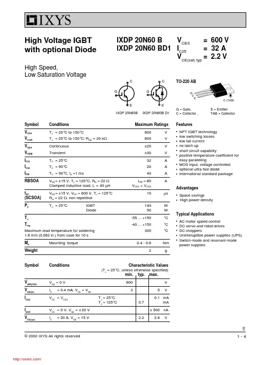
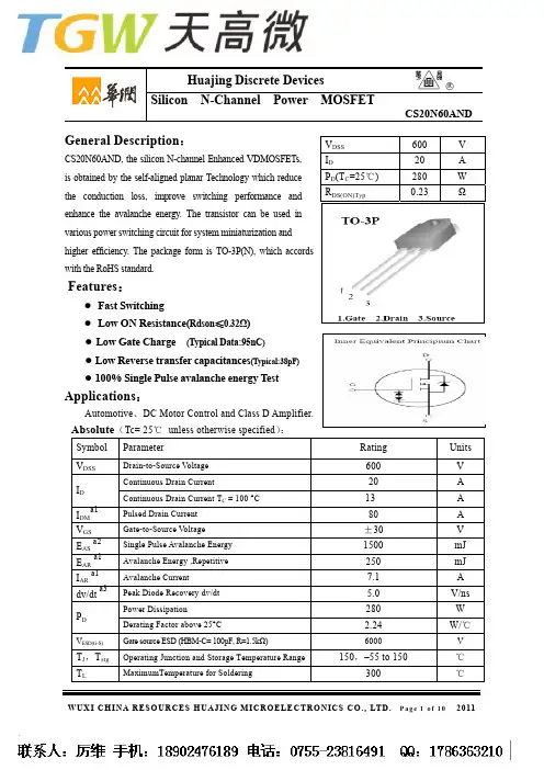
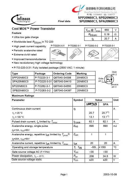
20N60C
- 格式:pdf
- 大小:144.30 KB
- 文档页数:8
HGTG20N60C3, HGTP20N60C3,HGT1S20N60C3S45A, 600V, UFS Series N-Channel IGBTThis family of MOS gated high voltage switching devices combining the best features of MOSFETs and bipolar transistors. These devices have the high input impedance of a MOSFET and the low on-state conduction loss of a bipolar transistor. The much lower on-state voltage drop varies only moderately between 25o C and 150o C.The IGBT is ideal for many high voltage switching applications operating at moderate frequencies where low conduction losses are essential, such as: AC and DC motor controls, power supplies and drivers for solenoids, relays and contactors.Formerly developmental type TA49178.Symbol Features•45A, 600V, T C = 25o C•600V Switching SOA Capability•Typical Fall Time. . . . . . . . . . . . . . . . 108ns at T J = 150o C •Short Circuit Rating•Low Conduction Loss•Related Literature-TB334 “Guidelines for Soldering Surface MountComponents to PC Boards”PackagingJEDEC STYLE TO-247JEDEC TO-220AB (ALTERNATE VERSION)JEDEC TO-263ABOrdering InformationPART NUMBER PACKAGE BRAND HGTG20N60C3TO-247G20N60C3HGTP20N60C3TO-220AB G20N60C3HGT1S20N60C3S TO-263AB G20N60C3NOTE:When ordering, use the entire part number. Add the suffix 9A to obtain the TO-263AB variant in the tape and reel, i.e.,HGT1S20N60C3S9A.CEGGCECOLLECTOR(FLANGE)GCECOLLECTOR(FLANGE)GCOLLECTORE(FLANGE)INTERSIL CORPORATION IGBT PRODUCT IS COVERED BY ONE OR MORE OF THE FOLLOWING U.S. PATENTS4,364,0734,417,3854,430,7924,443,9314,466,1764,516,1434,532,5344,587,713 4,598,4614,605,9484,620,2114,631,5644,639,7544,639,7624,641,1624,644,637 4,682,1954,684,4134,694,3134,717,6794,743,9524,783,6904,794,4324,801,986 4,803,5334,809,0454,809,0474,810,6654,823,1764,837,6064,860,0804,883,767 4,888,6274,890,1434,901,1274,904,6094,933,7404,963,9514,969,027Data Sheet December 2001Absolute Maximum Ratings T C = 25o C, Unless Otherwise SpecifiedALL TYPES UNITS Collector to Emitter Voltage. . . . . . . . . . . . . . . . . . . . . . . . . . . . . . . . . . . . . . . . . . . . . .BV CES600V Collector Current ContinuousAt T C = 25o C . . . . . . . . . . . . . . . . . . . . . . . . . . . . . . . . . . . . . . . . . . . . . . . . . . . . . . . . .I C2545A At T C = 110o C . . . . . . . . . . . . . . . . . . . . . . . . . . . . . . . . . . . . . . . . . . . . . . . . . . . . . . .I C11020A Collector Current Pulsed (Note 1) . . . . . . . . . . . . . . . . . . . . . . . . . . . . . . . . . . . . . . . . . . . I CM300A Gate to Emitter Voltage Continuous. . . . . . . . . . . . . . . . . . . . . . . . . . . . . . . . . . . . . . . . .V GES±20V Gate to Emitter Voltage Pulsed . . . . . . . . . . . . . . . . . . . . . . . . . . . . . . . . . . . . . . . . . . . .V GEM±30V Switching Safe Operating Area at T J = 150o C (Figure 2) . . . . . . . . . . . . . . . . . . . . . . . SSOA20A at 600VPower Dissipation Total at T C = 25o C . . . . . . . . . . . . . . . . . . . . . . . . . . . . . . . . . . . . . . . . .P D164W Power Dissipation Derating T C > 25o C . . . . . . . . . . . . . . . . . . . . . . . . . . . . . . . . . . . . . . . . . . 1.32W/o C Reverse Voltage Avalanche Energy. . . . . . . . . . . . . . . . . . . . . . . . . . . . . . . . . . . . . . . . .E ARV100mJ Operating and Storage Junction Temperature Range . . . . . . . . . . . . . . . . . . . . . . . . T J, T STG-55 to 150o C Maximum Temperature for SolderingLeads at 0.063in (1.6mm) from Case for 10s. . . . . . . . . . . . . . . . . . . . . . . . . . . . . . . . . . T L Package Body for 10s, see Tech Brief 334. . . . . . . . . . . . . . . . . . . . . . . . . . . . . . . . . . .T pkg 300260o Co CShort Circuit Withstand Time (Note 2) at V GE = 12V. . . . . . . . . . . . . . . . . . . . . . . . . . . . . .t SC4µsShort Circuit Withstand Time (Note 2) at V GE = 10V. . . . . . . . . . . . . . . . . . . . . . . . . . . . . .t SC10µs CAUTION: Stresses above those listed in “Absolute Maximum Ratings” may cause permanent damage to the device. This is a stress only rating and operation of the device at these or any other conditions above those indicated in the operational sections of this specification is not implied.NOTES:1.Pulse width limited by maximum junction temperature.2.V CE(PK) = 360V, T J = 125o C, R G = 10Ω.Electrical Specifications T C = 25o C, Unless Otherwise SpecifiedPARAMETER SYMBOL TEST CONDITIONS MIN TYP MAX UNITS Collector to Emitter Breakdown Voltage BV CES I C = 250µA, V GE = 0V600--V Emitter to Collector Breakdown Voltage BV ECS I C = 10mA, V GE = 0V1528-V Collector to Emitter Leakage Current I CES V CE = BV CES T C = 25o C--250µAT C = 150o C-- 5.0mACollector to Emitter Saturation Voltage V CE(SAT)I C = I C110V GE = 15V T C = 25o C- 1.4 1.8V T C = 150o C- 1.5 1.9VGate to Emitter Threshold Voltage V GE(TH)I C = 250µA, V CE = V GE 3.4 4.8 6.3V Gate to Emitter Leakage Current I GES V GE = ±20V--±250nASwitching SOA SSOA T J = 150o C, R G =10Ω, V GE = 15V,L = 100µH V CE = 480V120--A V CE = 600V20--AGate to Emitter Plateau Voltage V GEP I CE = I C110, V CE = 0.5 BV CES-8.4-VOn-State Gate Charge Q G(ON)I CE = I C110V CE = 0.5 BV CES V GE = 15V-91110nC V GE = 20V-122145nCCurrent Turn-On Delay Time t d(ON)I IGBT and Diode at T J = 25o CI CE = I C110V CE = 0.8 BV CESV GE = 15VR G = 10ΩL = 1mHTest Circuit (Figure 17)-2832nsCurrent Rise Time t rI-2428ns Current Turn-Off Delay Time t d(OFF)I-151210ns Current Fall Time t fI-5598ns Turn-On Energy (Note 4)E ON1-295320µJ Turn-On Energy (Note 4)E ON2-500550µJ Turn-Off Energy (Note 3)E OFF-500700µJCurrent Turn-On Delay Time t d(ON)I IGBT and Diode at T J = 150o C I CE = I C110V CE = 0.8 BV CES V GE = 15V R G = 10ΩL = 1mHTest Circuit (Figure 17)-2832ns Current Rise Timet rI -2428ns Current Turn-Off Delay Time t d(OFF)I -280450ns Current Fall Time t fI -108210ns Turn-On Energy (Note 4)E ON1-380410µJ Turn-On Energy (Note 4)E ON2- 1.0 1.1mJ Turn-Off Energy (Note 3)E OFF - 1.2 1.7mJThermal Resistance Junction To Case R θJC--0.76o C/WNOTES:3.T urn-Off Energy Loss (E OFF ) is defined as the integral of the instantaneous power loss starting at the trailing edge of the input pulse and ending at the point where the collector current equals zero (I CE = 0A). All devices were tested per JEDEC Standard No. 24-1 Method for Measurement of Power Device Turn-Off Switching Loss. This test method produces the true total Turn-Off Energy Loss.4.Values for two T urn-On loss conditions are shown for the convenience of the circuit designer. E ON1 is the turn-on loss of the IGBT only. E ON2 is the turn-on loss when a typical diode is used in the test circuit and the diode is at the same T J as the IGBT . The diode type is specified in Figure 17.Typical Performance CurvesUnless Otherwise SpecifiedFIGURE 1.DC COLLECTOR CURRENT vs CASETEMPERATUREFIGURE 2.MINIMUM SWITCHING SAFE OPERATING AREAFIGURE 3.OPERATING FREQUENCY vs COLLECTOR TOEMITTER CURRENTFIGURE 4.SHORT CIRCUIT WITHSTAND TIMEElectrical SpecificationsT C = 25o C, Unless Otherwise Specified (Continued)PARAMETERSYMBOL TEST CONDITIONSMIN TYP MAX UNITS T C , CASE TEMPERATURE (o C)I C E , D C C O L L E C T O R C U R R E N T (A )50V GE = 15V257510012515050301020400V CE , COLLECTOR TO EMITTER VOLTAGE (V)6070040I C E , C O L L E C T O R T O E M I T T E R C U R R E N T (A )20300400200100500600080100120140T J = 150o C, R G = 10Ω, V GE = 15V, L = 100µH0f M A X , O P E R A T I N G F R E Q U E N C Y (k H z )2I CE , COLLECTOR TO EMITTER CURRENT (A)1051100401020f MAX1 = 0.05 / (t d(OFF)I + t d(ON)I )R ØJC = 0.76o C/W, SEE NOTES P C = CONDUCTION DISSIPATION (DUTY FACTOR = 50%)f MAX2 = (P D - P C ) / (E ON2 + E OFF )T C V GE 110o C 10V15V 75o C 110o C 75o C10V 15V T J = 150o C, R G = 10Ω, L = 1mH, V CE = 480VV GE , GATE TO EMITTER VOLTAGE (V)I S C , P E A K S H O R T C I R C U I T C U R R E N T (A )t S C , S H O R T C I R C U I T W I T H S T A N D T I M E (µs )1011121314152468150200250300350t SCI SC101214400450V CE = 360V, R G = 10Ω, T J = 125o CFIGURE 5.COLLECTOR TO EMITTER ON-STATE VOLTAGE FIGURE 6.COLLECTOR TO EMITTER ON-STATE VOLTAGEFIGURE 7.TURN-ON ENERGY LOSS vs COLLECTOR TOEMITTER CURRENT FIGURE 8.TURN-OFF ENERGY LOSS vs COLLECTOR TOEMITTER CURRENTFIGURE 9.TURN-ON DELAY TIME vs COLLECTOR TOEMITTER CURRENT FIGURE 10.TURN-ON RISE TIME vs COLLECTOR TOEMITTER CURRENT2V CE , COLLECTOR TO EMITTER VOLTAGE (V)I C E , C O L L E C T O R T O E M I T T E R C U R R E N T (A )02084806040100610PULSE DURATION = 250µsDUTY CYCLE <0.5%, V GE = 10V T C = -55o CT C = 150o CT C = 25o CI C E , C O L L E C T O R T O E M I T T E R C U R R E N T (A )V CE , COLLECTOR TO EMITTER VOLTAGE (V)15020025030002305014100DUTY CYCLE <0.5%, V GE = 15V PULSE DURATION = 250µsT C = 150o CT C = -55o CT C = 25o C56E O N 2, T U R N -O N E N E R G Y L O S S (m J )2.51.5I CE , COLLECTOR TO EMITTER CURRENT (A)2.01.00.52010251553.00303540T J = 25o C, T J = 150o C, V GE = 15VT J = 25o C, T J = 150o C, V GE = 10VR G = 10Ω, L = 1mH, V CE = 480V3.54.0I CE , COLLECTOR TO EMITTER CURRENT (A)E OF F , T U R N -O F F E N E RG Y L O S S (m J )0.52520101551.02.52.01.53035403.0T J = 25o C; V GE = 10V OR 15VT J = 150o C; V GE = 10V OR 15VR G = 10Ω, L = 1mH, V CE = 480V I CE , COLLECTOR TO EMITTER CURRENT (A)t d I ,T U R N -O N D E L A Y T I M E (n s )20101552530354040302035254550R G = 10Ω, L = 1mH, V CE = 480VT J = 25o C, T J = 150o C, V GE = 15VT J = 25o C, T J = 150o C, V GE = 10VI CE , COLLECTOR TO EMITTER CURRENT (A)t r I ,R I S E T I M E (n s )2505075125100150101554030203525175200T J = 25o C AND T J = 150o C, V GE = 15VT J = 25o C, T J = 150o C, V GE = 10VR G = 10Ω, L = 1mH, V CE = 480VFIGURE 11.TURN-OFF DELAY TIME vs COLLECTOR TOEMITTER CURRENT FIGURE 12.FALL TIME vs COLLECTOR TO EMITTERCURRENTFIGURE 13.TRANSFER CHARACTERISTIC FIGURE 14.GATE CHARGE WAVEFORMSFIGURE 15.CAPACITANCE vs COLLECTOR TO EMITTER VOLTAGE101525525020100175125150200225I CE , COLLECTOR TO EMITTER CURRENT (A)t d (O F F )I , T U R N -O F F D E L A Y T I M E (n s )303540R G = 10Ω, L = 1mH, V CE = 480VT J = 150o C, V GE = 10V , V GE = 15VT J = 25o C, V GE = 10V, V GE = 15V 275300I CE , COLLECTOR TO EMITTER CURRENT (A)t f I , F A L L T I M E (n s )608010040507090102025515303540R G = 10Ω, L = 1mH, V CE = 480V110120T J = 150o C, V GE = 10V OR V GE = 15VT J = 25o C, V GE = 10V OR 15VI C E , C O L L E C T O R T O E M I T T E R C U R R E N T (A )501001505789106V GE , GATE TO EMITTER VOLTAGE (V)1120025030012131415PULSE DURATION = 250µsDUTY CYCLE <0.5%, V CE = 10V T C = 150o CT C = 25o CT C = -55o CQ g , GATE CHARGE (nC)08106420102040V G E , G A T E T O E M I T T E R V O L T A G E (V )5010030121416I G (REF) = 1mA, R L = 15Ω, T C = 25o CV CE = 400VV CE = 200VV CE = 600V60708090V CE , COLLECTOR TO EMITTER VOLTAGE (V)5101520250C , C A P A C I T A N C E (n F )12345C IESC OESC RESFREQUENCY = 1MHzFIGURE 16.NORMALIZED TRANSIENT THERMAL RESPONSE, JUNCTION TO CASETest Circuit and WaveformsFIGURE 17.INDUCTIVE SWITCHING TEST CIRCUIT FIGURE 18.SWITCHING TEST WAVEFORMSt 1,RECTANGULAR PULSE DURATION (s)Z θJ C ,N O R M A L I Z E D T H E R M A L R E S P O N S E10-310-210-110010-510-310-210-110010110-40.10.20.050.02SINGLE PULSEt 1t 2P DDUTY FACTOR, D = t 1 / t 2PEAK T J = (P D X Z θJC X R θJC ) + T C0.50.01R G = 10ΩL = 1mHV DD = 480V+-RHRP3060t fIt d(OFF)It rI t d(ON)I10%90%10%90%V CEI CEV GEE OFFE ON2Handling Precautions for IGBTsInsulated Gate Bipolar T ransistors are susceptible togate-insulation damage by the electrostatic discharge of energy through the devices. When handling these devices, care should be exercised to assure that the static charge built in the handler’s body capacitance is not discharged through the device. With proper handling and application procedures, however, IGBTs are currently being extensively used in production by numerous equipment manufacturers in military, industrial and consumer applications, with virtually no damage problems due to electrostatic discharge. IGBTs can be handled safely if the following basic precautions are taken:1.Prior to assembly into a circuit, all leads should be keptshorted together either by the use of metal shortingsprings or by the insertion into conductive material such as “ECCOSORBD™ LD26” or equivalent.2.When devices are removed by hand from their carriers,the hand being used should be grounded by any suitable means - for example, with a metallic wristband.3.Tips of soldering irons should be grounded.4.Devices should never be inserted into or removed fromcircuits with power on.5.Gate Voltage Rating - Never exceed the gate-voltagerating of V GEM. Exceeding the rated V GE can result in permanent damage to the oxide layer in the gate region.6.Gate Termination - The gates of these devices areessentially capacitors. Circuits that leave the gate open-circuited or floating should be avoided. These conditions can result in turn-on of the device due to voltage buildup on the input capacitor due to leakage currents or pickup.7.Gate Protection - These devices do not have an internalmonolithic Zener diode from gate to emitter. If gateprotection is required an external Zener is recommended.Operating Frequency InformationOperating frequency information for a typical device (Figure3) is presented as a guide for estimating device performance for a specific application. Other typical frequency vs collector current (I CE) plots are possible using the information shown for a typical unit in Figures 5, 6, 7, 8, 9 and 11. The operating frequency plot (Figure 3) of a typical device shows f MAX1 or f MAX2; whichever is smaller at each point. The information is based on measurements of a typical device and is bounded by the maximum rated junction temperature.f MAX1 is defined by f MAX1 = 0.05/(t d(OFF)I+ t d(ON)I). Deadtime (the denominator) has been arbitrarily held to 10% of the on-state time for a 50% duty factor. Other definitions are possible. t d(OFF)I and t d(ON)I are defined in Figure 18. Device turn-off delay can establish an additional frequency limiting condition for an application other than T JM. t d(OFF)I is important when controlling output ripple under a lightly loaded condition.f MAX2 is defined by f MAX2 = (P D - P C)/(E OFF + E ON2). The allowable dissipation (P D) is defined by P D = (T JM - T C)/RθJC. The sum of device switching and conduction losses must not exceed P D. A 50% duty factor was used (Figure 3) and the conduction losses (P C) are approximated byP C=(V CE x I CE)/2.E ON2 and E OFF are defined in the switching waveforms shown in Figure 18. E ON2 is the integral of the instantaneous power loss (I CE x V CE) during turn-on and E OFF is the integral of the instantaneous power loss(I CE x V CE) during turn-off. All tail losses are included in the calculation for E OFF; i.e., the collector current equals zero (I CE = 0).。