
C106DG中文资料
- 格式:pdf
- 大小:130.48 KB
- 文档页数:6


MOTOROLA
SEMICONDUCTOR TECHNICAL DATA
3–26REV 5© Motorola, Inc. 19963/93Triple 4-3-3-Input NOR Gate
The MC10106 is a triple 4–3–3 input NOR gate.
PD= 30 mW typ/gate (No Load)
tpd= 2.0 ns typ
tr, tf= 2.0 ns typ (20%–80%)
LOGIC DIAGRAM
VCC1= PIN 1
VCC2= PIN 16
VEE= PIN 81412
1315119
10275364MC10106
DIP
PIN ASSIGNMENT
VCC1
BOUT
AOUT
AIN
AIN
AIN
AIN
VEEVCC2
COUT
CIN
CIN
CIN
BIN
BIN
BIN16
15
14
13
12
11
10
91
2
3
4
5
6
7
8
Pin assignment is for Dual–in–Line Package.
For PLCC pin assignment, see the Pin Conversion
Tables on page 6–11 of the Motorola MECL Data
Book (DL122/D).L SUFFIX
CERAMIC PACKAGE
CASE 620–10
P SUFFIX
PLASTIC PACKAGE
CASE 648–08
FN SUFFIX
PLCC
CASE 775–02元器件交易网
MC10106
3–27MOTOROLAMECL Data
DL122 — Rev 6ELECTRICAL CHARACTERISTICS
PiTest Limits
Pin–30°C+25°C+85°C
CharacteristicSymbolUnder
TestMinMaxMinTypMaxMinMaxUnit
Power Supply Drain CurrentIE823172123mAdc

D1S1NCDual-In-Line
IN1D3V–S3GNDS4VLD4V+NCIN2D2S212345678161514131211109
Top ViewDG5043Vishay Siliconix
Document Number: 70059S-52880—Rev. B, S FaxBack 408-970-56004-1Monolithic General-Purpose CMOS Analog Switch
FEATURESBENEFITSAPPLICATIONSD"15-V Input RangeDOn-Resistance: <50 WDBreak-Before-Make SwitchingDTTL and CMOS CompatibleDImproved Signal HeadroomDReduced Switching ErrorsDNo Shorting of InputsDSimple InterfacingDAudio SwitchingDInstrumentationDBattery Powered Systems
DESCRIPTION
The DG5043 solid state analog switch is recommended forgeneral purpose applications in instrumentation, and processcontrol. Built on the Vishay Siliconix PLUS-40 high voltageCMOS process, this device provides ease-of-use andperformance advantages to the system designer. Keyperformance features of the DG5043 are 1-ms switching, lowpower supply requirements, and break-before-makeswitching. Each switch conducts equally well in eitherdirection, when on, and blocks up to 30 V peak-to-peak whenoff. Off leakage current is 1-nA maximum. An epitaxial layerprevents latch up. For new designs, DG403 is recommended.
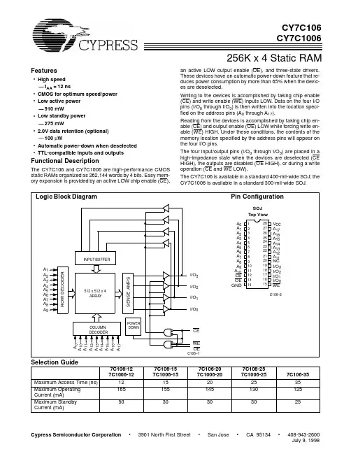
256K x 4 Static RAM CY7C106
CY7C1006
CypressSemiconductorCorporation•3901NorthFirstStreet•SanJose•CA 95134•408-943-2600
July 9, 1998Features
•High speed
—t
AA =
12 ns
•CMOS for optimum speed/power
•Low active power
—910 mW
•Low standby power
—275 mW
•2.0V data retention (optional)
—100 µW
•Automatic power-down when deselected
•TTL-compatible inputs and outputs
Functional Description
The CY7C106 and CY7C1006 are high-performance CMOS
static RAMs organized as 262,144 words by 4 bits. Easy mem-ory expansion is provided by an active LOW chip enable (CE),an active LOW output enable (OE), and three-state drivers.
These devices have an automatic power-down feature that re-
duces power consumption by more than 65% when the devic-
es are deselected.
Writing to the devices is accomplished by taking chip enable(CE) and write enable (WE) inputs LOW. Data on the four I/O

112/13/01Supertex Inc. does not recommend the use of its products in life support applications and will not knowingly sell its products for use in such applications unless it receives an adequate "products liabilityindemnification insurance agreement." Supertex does not assume responsibility for use of devices described and limits its liability to the replacement of devices determined to be defective due toworkmanship. No responsibility is assumed for possible omissions or inaccuracies. Circuitry and specifications are subject to change without notice. For the latest product specifications, refer to theSupertex website: . For complete liability information on all Supertex products, refer to the most current databook or to the Legal/Disclaimer page on the Supertex website.HV506Preliminary 80-Lead64-Lead 3-SidedCeramic GullwingPlastic GullwingDie