
2SK226资料
- 格式:pdf
- 大小:46.00 KB
- 文档页数:1

百度文库 - 好好学习,天天向上
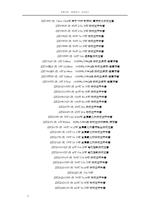
-1 2SK199N沟 15mA 100mW用于VHF射频段/高频放大场效应管
2SK1990N沟 450V 2.5A 30W场效应开关管
2SK1991N沟 500V 2.5A 30W场效应开关管
2SK1992N沟 450V 3A 35W场效应开关管
2SK1993N沟 500V 3A 35W场效应开关管
2SK1994N沟 900V 1A 30W场效应开关管
2SK1995N沟 900V 2A 35W场效应开关管
2SK1999N沟 120V 12A通用型场效应管
2SK19AN沟 18V 3-24mA 100MHz Nf=2dB场效应调频/甚高频管
2SK19-BLN沟 18V 12-24mA 100MHz Nf=2dB场效应调频/甚高频管
2SK19-GRN沟 18V 6-14mA 100MHz Nf=2dB场效应调频/甚高频管
2SK19TMN沟 18V 3-24mA 100MHz Nf=2dB场效应调频/甚高频管
2SK19-YN沟 18V 3-7mA 100MHz Nf=2dB场效应调频/甚高频管
2SK2002-01MN沟 600V 3A 30W场效应开关管
2SK2003-01MN沟 600V 4A 40W场效应开关管
2SK2004-01LN沟 1000V 4A 80W场效应开关管
2SK2004-01SN沟 1000V 4A 80W场效应开关管
2SK2007N沟 250V 20A场效应开关管
2SK2008N沟 250V 20A场效应开关管
2SK2009N沟 30V 0.2A 200mW金属氧化物场效应开关管
1
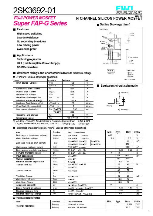
ItemSymbolRatingsUnitDrain-source voltageVDS450VDSX *5450Continuous drain currentID±17Pulsed drain currentID(puls]±68Gate-source voltageVGS±30Repetitive or non-repetitiveIAR *217Maximum Avalanche EnergyEAS *1221.9Maximum Drain-Source dV/dtdVDS/dt *420Peak Diode Recovery dV/dtdV/dt *35Max. power dissipationPD Ta=25°C2.02 Tc=25°C225Operating and storageTch+150temperature rangeTstg Electrical characteristics (Tc =25°C unless otherwise specified)
Thermalcharacteristics2SK3692-01FUJI POWER MOSFETN-CHANNEL SILICON POWER MOSFETFeaturesHigh speed switchingLow on-resistanceNo secondary breadownLow driving powerAvalanche-proofApplicationsSwitching regulatorsUPS (Uninterruptible Power Supply)DC-DC convertersMaximum ratings and characteristicAbsolute maximum ratings(Tc=25°C unless otherwise specified)
Item Symbol Test ConditionsZero gate voltage drain current IDSSVDS=450V VGS=0VVDS=360V VGS=0V VGS=±30V ID=8.5A VGS=10VID=8.5A VDS=25VVCC=300V ID=8.5AVGS=10VRGS=10 ΩMin. Typ. Max. UnitsVVµAnAΩSpF
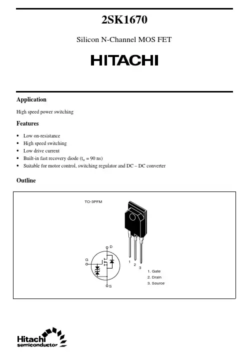
2SK1670Silicon N-Channel MOS FET
Application
High speed power switching
Features
• Low on-resistance
• High speed switching
• Low drive current
• Built-in fast recovery diode (trr = 90 ns)
• Suitable for motor control, switching regulator and DC – DC converter
Outline
TO-3PFM
1. Gate2. Drain3. SourceD
G
S1232SK1670
2Absolute Maximum Ratings (Ta = 25°C)
ItemSymbolRatingsUnit
Drain to source voltageVDSS250V
Gate to source voltageVGSS±30V
Drain currentID30A
Drain peak currentID(pulse)*1120A
Body to drain diode reverse drain currentIDR30A
Channel dissipationPch*260W
Channel temperatureTch150°C
Storage temperatureTstg–55 to +150°C
Notes1.PW ≤ 10 µs, duty cycle ≤ 1%2.Value at TC = 25°C2SK1670
3Electrical Characteristics (Ta = 25°C)
ItemSymbolMinTypMaxUnitTest conditions
Drain to source breakdownvoltageV(BR)DSS250——VID = 10 mA, VGS = 0

The information in this document is subject to change without notice. Before using this document, please
confirm that this is the latest version.
Not all devices/types available in every country. Please check with local NEC representative for
availability and additional information.MOS FIELD EFFECT TRANSISTOR
2SK3575
SWITCHING
N-CHANNEL POWER MOS FETDATA SHEET
Document No. D16261EJ2V0DS00 (2nd edition)
Date Published September 2002 NS CP(K)Printed in Japan
©
2002The mark ! shows major revised points.DESCRIPTION
The 2SK3575 is N-channel MOS FET device that
features a low on-state resistance and excellent switching
characteristics, designed for low voltage high current
applications such as DC/DC converter with synchronous
rectifier.
FEATURES
•4.5V drive available
•Low on-state resistance
R
DS(on)1 = 4.5 mΩ MAX. (V
GS = 10 V, I