Acr-Bis粉剂(30%,291)
- 格式:pdf
- 大小:181.61 KB
- 文档页数:1
关于ACR加工助剂的介绍一、PVC加工助剂简介加工助剂在国外最早由美国罗门哈斯(Rohm & Hass)公司于1958年首先开发成功,同年推出第一个牌号K-120。
此后,国外许多公司开始纷纷涉足这一领域,开发出相类似的产品。
70年代之后,随着PVC制品的迅速增长,加工助剂得到了广泛应用。
目前,国外主要生产厂家及相关产品有日本三菱(MITSUBSHI ROYAL)公司P系列、钟渊化学(KANEKA)PA系列、美国罗门哈斯(Rohm & Hass)公司K系列、德国熊牌(BEAR)F系列,阿托菲娜(ATOFINA) P系列,还有韩国LG化学的PA系列等。
国内较早从事PVC加工助剂研究的是北京化工研究院、山西化工研究所等。
上海珊瑚化工厂于80年代初最早实现工业化生产,推出的牌号国内统称为ACR201、ACR401。
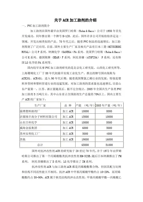
进入90年代后期,随着我国聚氯乙烯行业的发展,特别是塑料异型材和塑料管道行业的迅猛发展,对加工助剂的需求量也迅速增长,目前山东产量第一,江苏、浙江紧随其后。
据不完全统计,2005年全国共生产各类PVC 加工助剂5万吨左右,其中山东省占全国助剂生产总量的70%以上。
国内主要生产ACR的厂家如下:国外对抗冲改性剂ACR的研究始于20世纪70年代,并于1972年由罗姆哈斯公司推出了第一个丙烯酸酯类抗冲改性剂KM-323B。
随后日本钟渊推出了FM 系列,阿托菲娜推出了D系列,LG化学推出了IM系列。
抗冲改性剂ACR与加工助剂ACR都是丙烯酸酯聚合物,但因其配方比例和结构不同而性能大不相同,抗冲ACR中甲基丙烯酸甲酯约占10-20%,而丙烯酸酯约占80-90%。
ACR属于核壳结构的冲击改性剂,甲基丙烯酸甲酯—丙烯酸乙酯高聚物组成的外壳,以丙烯酸丁酯类交联形成的橡胶弹性体为核的链段分布于颗粒内层。
抗冲改性剂ACR象MBS一样同为核壳结构。
与MBS、CPE等抗冲改性剂相比,其加工性能和耐候性能好,表面光洁度高,尤其适用于户外制品,在国外,丙烯酸酯类抗冲改性剂因其环保,性能优良,耐候性能高已经取代CPE抗冲改性剂。
![sds缓冲液制备[详解]](https://uimg.taocdn.com/5aa5bd05a31614791711cc7931b765ce05087ae3.webp)
SDS-PAGE的试剂配置:000(a)浓缩胶缓冲液——1.0M pH 6.8的Tris-Hcl溶液:称取12.11g Tris 置于100ml 的容量瓶中,加入约80ml 去离子水,充分搅拌溶解;用盐酸调节pH值至6.8后,将溶液定容,室温下保存备用。
0000(b)分离胶缓冲溶液——1.5M pH 8.8的Tris-Hcl溶液:称取18.17g Tris于100ml的容量瓶中,加入约80ml去离子水,充分搅拌溶解;用盐酸调节至8.8后,将溶液定容保存。
000(c)SDS上样缓冲液:取0.063ml pH 6.8的Tris-Hcl缓冲液与5ml 的容量瓶中,依次加入0.1g十二烷基环酸钠SDS、5.0mg溴酚蓝BPB 和0.5ml甘油;加入适量去离子水搅拌溶解后,定容至5 ml;小份(1 ml/份)分装后,在-20℃下保存备用。
000(d)SDS-PAGE 电泳缓冲液:称取3.02g 三羟甲基氨基甲烷(Tris)于 1 L 的容量瓶中,加入18.8 g 甘氨酸(Glycine)和 1.0 g SDS;加去离子水溶解并混合均匀后,定容至 1 L,室温下保存备用。
0 00(e)30%丙烯酰胺溶液:称取29.0 g 丙烯酰胺(Acr)和1.0 N, N′-亚甲基双丙烯酰胺(Bis)于100 ml 棕色的容量瓶中,加去离子水溶解并混匀后定容,放置于4℃下保存备用。
0000(f)10%(W/V)SDS 溶液:称取10.0 g SDS 于100 ml 的容量瓶中,加入约80 ml 去离子水;在68 ℃的水浴中加热溶解,自然冷却至室温;加去离子水定容并,室温下保存备用。
000(g)10% (W/V)APS 溶液:称取0.1g 过硫酸铵(APS),置于1.5ml 离心管中,加去离子水1 ml 溶解即可;4℃保存备用。
000(h)考马斯亮蓝染色液:称取0.5 g 考马斯亮蓝R 250 于500ml 的容量瓶中,加入约225 ml 甲醇和50 ml 乙酸;充分搅拌溶解后,加入去离子水定容,室温下保存备用。
影楼第三节课笔记ACR一、影楼修片流程1.预处理:保证基本曝光,明暗层次,白平衡,饱和度等基本参数,根据个人审美调色等。
(70%)2.细节精修:瑕疵,穿帮,液化,磨皮,局部调整等(30%)二、ACR介绍Adobe camera raw 内嵌于PS和LR中,可处理不同相机生成的raw格式原片;版本越高,兼容度越好。
目前版本是12.2--- 2020年05月12日推荐使用:Ps使用CC2018及以上,可以点击ps帮助-更新,更新你的版本。
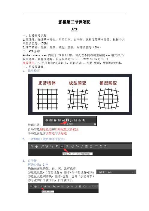
三、照片预处理1.镜头校正处理办法:自动勾选删除色差和启用配置文件校正手动里面包含去紫边与去绿边2.二次构图(裁剪和水平拉直):3.白平衡解决办法:3种确保画面里的黑、白、灰,没有色彩①原照设置-(自动设置):基本-白平衡设置-自动②色温及色调滑块:基本-色温、色调(手动调节)③专业的白平衡工具:白平衡工具4.曝光、黑白场:理想的黑白场是照片中白色很高亮,黑色很暗沉,整个照片每个色阶段都有信息,高光内白色接近或刚刚达到纯白,阴影黑色接近或刚刚达到纯黑。
解决方法:1.调整整体曝光 2.定位黑色 3.定位白色5.适当的色彩:要想调色必须给与颜色,raw格式原片整体色彩偏灰,饱和偏低,调色之前增加适当的饱和度,让色彩更艳丽,为后期调色做好准备!要想调色,必须予色-------根据需要调节①自然饱和度②色相饱和度6.适当的锐化与降噪:降噪是去除杂色,会使画面平滑,模糊;锐化是调整图像边缘细节的对比度,并在边缘的两侧生成一条亮线一条暗线,使画面整体更加清晰。
(老照片修复经常使用降噪)噪点分两种:颜色杂色和明亮度杂色1.颜色噪点产生的原因:高感光度iso下拍摄导致2.明亮度噪点产生原因:长曝光时间拍摄,传感器散热不通畅造成3.曝光不足的片子提亮也会产生噪点7.暗角:①镜头造成的暗角;②后期添加的暗角效果四周压暗,让主体更突出,更聚焦!。
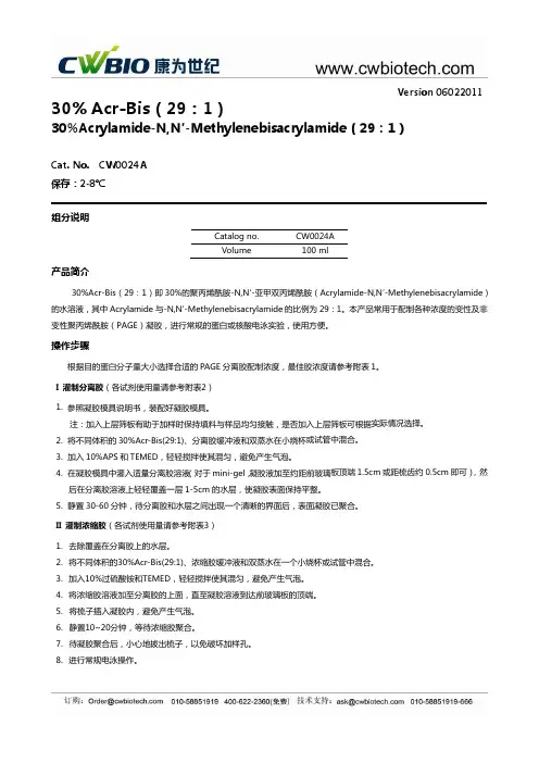
Version 0602201130% Acr-Bis(29:1)30%Acrylamide-N,N′-Methylenebisacrylamide(29:1)Cat. No. CW0024A保存:2-8℃ 组分说明Catalog no. CW0024A Volume100 ml产品简介本产品常用于配制各种浓度的变性及非酰胺(PAGE)凝胶,进行常规的蛋白或核酸电泳实验,使用方便。
操作步骤 分离胶配制浓度,最佳胶浓度请参考附表1。
1. 实际情况选择。
或试管中混合。
板顶端1.5cm 或距梳齿约0.5cm 即可), 然 杯或试管中混合。
凝胶溶液到达前玻璃板的顶端。
拔出梳子,以免破坏加样孔。
8. 进行常规电泳操作。
30%Acr-Bis(29:1)即30%的聚丙烯酰胺-N,N′-亚甲双丙烯酰胺(Acrylamide-N,N′-Methylenebisacrylamide)的水溶液,其中Acrylamide 与-N,N′-Methylenebisacrylamide 的比例为29:1。
变性聚丙烯根据目的蛋白分子量大小选择合适的PAGE I 灌制分离胶(各试剂使用量请参考附表2) 参照凝胶模具说明书,装配好凝胶模具。
注:加入上层筛板有助于加样时保持填料与样品均匀接触,是否加入上层筛板可根据2. 将不同体积的30%Acr-Bis(29:1)、分离胶缓冲液和双蒸水在小烧杯3. 加入10%APS 和TEMED,轻轻搅拌使其混匀,避免产生气泡。
4. 在凝胶模具中灌入适量分离胶溶液(对于mini-gel,凝胶液加至约距前玻璃后在分离胶溶液上轻轻覆盖一层1-5cm 的水层,使凝胶表面保持平整。
5. 静置30-60分钟,待分离胶和水层之间出现一个清晰的界面后,表面凝胶已聚合。
II 灌制浓缩胶(各试剂使用量请参考附表3)1. 去除覆盖在分离胶上的水层。
2. 将不同体积的30%Acr-Bis(29:1)、浓缩胶缓冲液和双蒸水在一个小烧3. 加入10%过硫酸铵和TEMED,轻轻搅拌使其混匀,避免产生气泡。
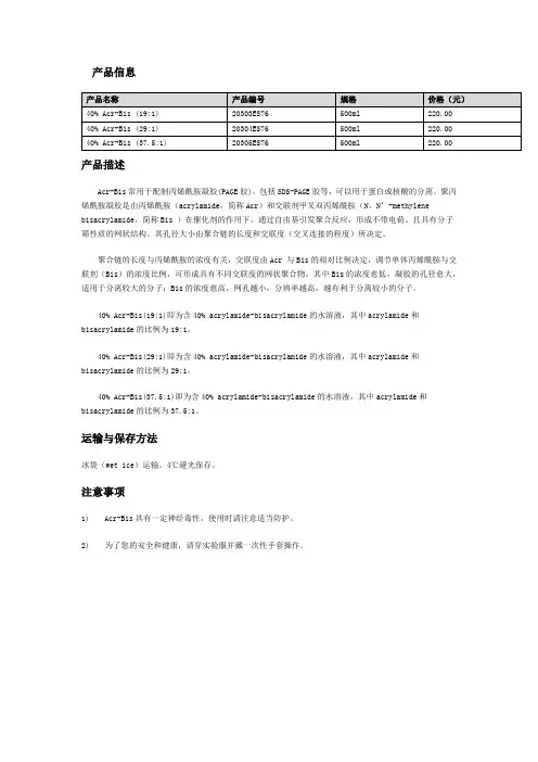
产品信息产品描述Acr-Bis常用于配制丙烯酰胺凝胶(PAGE胶),包括SDS-PAGE胶等,可以用于蛋白或核酸的分离。
聚丙烯酰胺凝胶是由丙烯酰胺(acrylamide,简称Acr)和交联剂甲叉双丙烯酰胺(N,N’-methylene bisacrylamide,简称Bis )在催化剂的作用下,通过自由基引发聚合反应,形成不带电荷、且具有分子筛性质的网状结构。
其孔径大小由聚合链的长度和交联度(交叉连接的程度)所决定。
聚合链的长度与丙烯酰胺的浓度有关,交联度由Acr 与Bis的相对比例决定,调节单体丙烯酰胺与交联剂(Bis)的浓度比例,可形成具有不同交联度的网状聚合物。
其中Bis的浓度愈低,凝胶的孔径愈大,适用于分离较大的分子;Bis的浓度愈高,网孔越小,分辨率越高,越有利于分离较小的分子。
40% Acr-Bis(19:1)即为含40% acrylamide-bisacrylamide的水溶液,其中acrylamide和bisacrylamide的比例为19:1。
40% Acr-Bis(29:1)即为含40% acrylamide-bisacrylamide的水溶液,其中acrylamide和bisacrylamide的比例为29:1。
40% Acr-Bis(37.5:1)即为含40% acrylamide-bisacrylamide的水溶液,其中acrylamide和bisacrylamide的比例为37.5:1。
运输与保存方法冰袋(wet ice)运输。
4℃避光保存。
注意事项1)Acr-Bis具有一定神经毒性,使用时请注意适当防护。
2)为了您的安全和健康,请穿实验服并戴一次性手套操作。
The Polyacrylamide MatrixThe polymerization of a polyacrylamide matrix withmethylenebisacrylamide cross-linking.Polyacrylamide gels are formed by the polymerization of acrylamide in aqueous solution in the presence of small amounts of a bifunctional crosslinker. The crosslinker is usuallymethylene:bisacrylamide (bis, or MBA). The copolymerization of acrylamide with methylenebisacrylamide produces a mesh-like network in three dimensions, consisting of acrylamide chains with interconnections formed from the methylenebisacrylamide. A variety of crosslinkers are available in addition to bis. These include piperazine diacrylate (PDA), N,N'-bisacrylylcystamine (BAC), and N,N'-diallyltartardiamide (DATD). PDA is used to reduce silver stain backgrounds in SDS-PAGE gels. BAC and DATD are both disruptable cross-linkers which enable gels to be solubilized.BAC, DATD, and Piperazine diacrylate are sometimes usedas the cross-linkers in polyacrylamide gels to vary thephysical or chemical properties of the gel.For discussions of the composition of polyacrylamide gels, a standard nomenclature has been widely adopted. In this nomenclature, T represents the total percentage concentration (w/v) of monomer (acrylamide plus crosslinker) in the gel. The term C refers to the percentage of the total monomer represented by the crosslinker. For example, an 8%, 19:1 (acrylamide/bisacrylamide) gel would have a T value of 8% and a C value of 5%.Upon the introduction of catalyst, the polymerization of acrylamide and methylene bisacrylamide proceeds via a free-radical mechanism. The most common system of catalytic initiation involves the production of free oxygen radicals by ammonium persulfate in the presence of the tertiary aliphatic amine N,N,N',N'-tetramethylethylenediamine (TEMED). Another catalytic system involves the generation of free radicals via a photochemical process using a very small amount of riboflavin in the presence of TEMED. In both catalytic systems, the presence of excess oxygen will inhibit the polymerization elongation process and can lead to shorter average chain length. For this reason, if the casting solution has been excessively agitated, deaeration under vacuum with a magnetic stirrer is suggested prior to addition of initiators.For certain applications, polyacrylamide has definite advantages compared to agarose. In an agarose gel, the pore size is large, so molecular sieving, i.e. separation by size, will not occur for smaller DNA fragments and most proteins. Additionally, by altering the total concentration of monomer in the gel and the ratio of acrylamide to bis, the pore size with a polyacrylamide gel can be altered in a reproducible manner. The small and reproducible pore size in polyacrylamide gels results in superior resolution: a 0.1% difference in size (1 base difference in a 1kb molecule) can be detected. Also, because acrylamide and bis are synthetic chemicals, there are virtually no batch to batch differences (It should be mentioned that batch to batch differences with agarose are overcome with the highest quality agaroses, such as National Diagnostics' AquaPor agaroses).Control of the pore size of a polyacrylamide gel is accomplished by changing the T and C values. With increasing T, the pore size decreases in a nearly linear relationship. Higher percentage gels (higher T), with smaller pores, are used to separate smaller molecules. The relationship of C to pore size is more complex. Generally, the minimum pore size occurs when C is about 5% (a 19:1 gel). Decreasing C results in a more open pore structure because there are fewer crosslinker molecules. Increasing C beyond 5% also increases the pore size. This appears to be because of nonhomogeneous bundling of strands in the gel.Researchers have settled on C values of 5.0% (19:1 acrylamide/bis) for most forms of denaturing DNA and RNA electrophoresis and 3.3% (29:1) for most native DNA and RNA gels. For SDS-PAGE electrophoresis of proteins, the standard C value that has been adopted is 2.6% (37.5:1). The table below gives recommended acrylamide/bis ratios and gel percentages for different molecular size ranges.。
来源于:注塑财富网
浅析ACR在PVCU加工过程中的作用
一、认识ACR(ACE)
ACR是丙烯酸脂共聚物,它是由MMA(甲基丙烯酸甲脂)与多种丙烯酸脂接脂共聚而成。
ACR-201是由MMA与EA(丙烯酸乙脂)组成;ACR-301是由MMA与EA和BA (丙烯酸丁脂)组成;ACR-401是由MMA与BA、BMA(甲基丙烯酸丁脂)和EMA(甲基丙烯酸乙脂)组成。
应该说它们都具有核壳结构。
二、ACR(ACE)在PVC加工过程中的作用
PVC在加工过程中应添加PVC树脂的1~5%的加工助剂,ACR(ACE)是应用最多的加工助剂,它在挤出、注塑、吹塑、吸塑和压延等PVCU的主要加工方法中得到了极为广泛的应用。
ACR(ACE)在PVCU加工过程中的作用机理是使PVC这种热稳定性差,塑化不良而又极易在加工时产生熔体破裂的树脂变得塑化良好,降低塑化温度,抑制熔体破裂,使产品具有较好的内在质量和面光泽性。
总之,它具有以下几点点作用:
1促进PVCU加工时的塑化性能,改善其流动性。
2改进PVCU热塑态的流变行为,提高熔体强度,避免熔体破裂,提高了制品的内在质量和表面光泽。
3具有长时间成型加工的稳定性。
4有效防止在挤出和注塑时由于挤压成型所产生的压力波动和流动伤痕用产生银丝等表面缺陷。
5促进发泡制品的泡孔均匀和细化。
6提高PVCU制品质量的一致性,如外观光泽、抗张强度、冲击强度及断裂伸长率等。
三、ACR(ACE)的新发展
如果在ACR中再有目的地引入一些活性单体,则可使ACR具有更高的改善PVCU加工性能的作用,且使PVCU产品具有更优良的抗冲性及其它综合性能。
注塑。

北京雷根生物技术有限公司
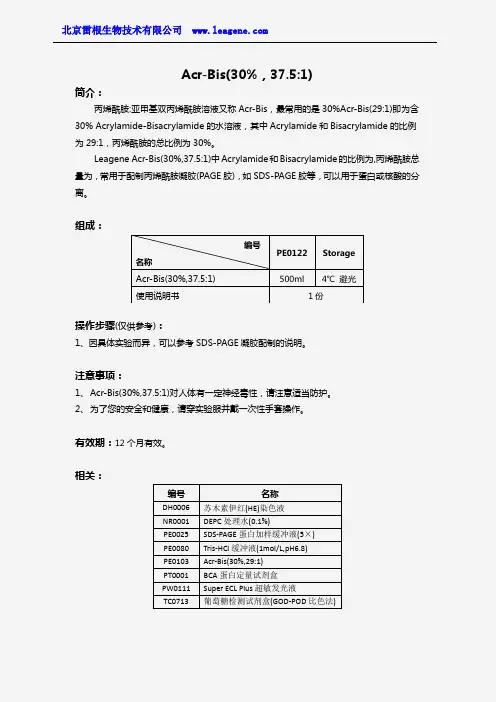
Acr-Bis(30%,37.5:1)
简介:
丙烯酰胺:亚甲基双丙烯酰胺溶液又称Acr-Bis ,最常用的是30%Acr-Bis(29:1)即为含30% Acrylamide-Bisacrylamide 的水溶液,其中Acrylamide 和Bisacrylamide 的比例为29:1,丙烯酰胺的总比例为30%。
Leagene Acr-Bis(30%,37.5:1)中Acrylamide 和Bisacrylamide 的比例为,丙烯酰胺总量为,常用于配制丙烯酰胺凝胶(PAGE 胶),如SDS-PAGE 胶等,可以用于蛋白或核酸的分离。
组成:
操作步骤(仅供参考):
1、因具体实验而异,可以参考SDS-PAGE 凝胶配制的说明。
注意事项:
1、 Acr-Bis(30%,37.5:1)对人体有一定神经毒性,请注意适当防护。
2、 为了您的安全和健康,请穿实验服并戴一次性手套操作。
有效期:12个月有效。
相关:
编号 名称 PE0122 Storage Acr-Bis(30%,37.5:1) 500ml 4℃ 避光 使用说明书
1份 编号 名称
DH0006 苏木素伊红(HE)染色液
NR0001 DEPC 处理水(0.1%)
PE0025 SDS-PAGE 蛋白加样缓冲液(5×)
PE0080 Tris-HCl 缓冲液(1mol/L,pH6.8)
PE0103 Acr-Bis(30%,29:1)
PT0001 BCA 蛋白定量试剂盒
PW0111 Super ECL Plus 超敏发光液
TC0713 葡萄糖检测试剂盒(GOD-POD 比色法)。
上海交通大学网络教育学院医学院分院生物化学技术课程习题册答案专业:检验技术层次:专升本绪论一、名词解释1.生物化学技术:是研究生物体的化学组成、结构、功能以及在生命活动中化学物质的代谢、调节控制等的实验方法。
2.盐溶:蛋白质、酶及其它们与其它物质的复合体在离子强度低的盐溶液中,其溶解度随着盐溶液浓度的升高而增加,此现象称为“盐溶”。
3.盐析:当溶液中盐浓度不断上升,达到一定程度,蛋白质等的溶解度反而逐渐减小,并先后从溶液中析出,称为“盐析”。
4.透析:利用溶液组分能否通过半透膜并由引起膜两边溶液的化学势能不同,而达到去除溶液中的小分子物质。
5.超滤(反向渗透):利用压力或离心力,迫使水和其他小的溶质分子通过半透膜,而蛋白质不能透过半透膜仍留在膜上。
6.凝胶层析法(Gel Chromatography):利用各种物质分子大小不同,在固定相上受到阻滞程度不同而达到分离的一种层析方法。
二、单选题1.凝胶层析不可应用于:( B )A. 脱盐B. 一步分离纯化生物大分子物质C. 高分子溶液的浓缩D. 测定高分子物质的分子量 E.分离分子大小不同的物质2.核酸在紫外区有强吸收,其最大吸收值是在波长:( C )A.206nm B.240nm C.260nm D.280nm E.304nm3.对260nm波长的紫外有强吸收主要是因为( E )A.核糖的环式结构 B.脱氧核糖的环式结构C.嘌呤的双环结构 D.嘧啶的单环结构 E. 嘌呤和嘧啶环中的共轭双键4.蛋白质在紫外区有强吸收,其最大吸收值是在波长:( D )A.206nm B.240nm C.260nm D.280nm E.304nm5.用紫外分光光度法测定蛋白质,因为蛋白质在紫外区有个最大吸收峰,其峰值波长是:D A.220nm B.245nm C.260nm D.280nm E.340nm6.用吸收光谱法测量双链DNA的含量为:( A )A.C(ug/ml)=A260×50×稀释倍数B.C(ug/ml)=A260×40×稀释倍数C.C(ug/ml)=A260×30×稀释倍数D.C(ug/ml)=A260×20×稀释倍数E.C(ug/ml)=A260×10×稀释倍数7.用吸收光谱法测量单链DNA的含量为:( B )A.C(ug/ml)=A260×50×稀释倍数B.C(ug/ml)=A260×40×稀释倍数C.C(ug/ml)=A260×30×稀释倍数D.C(ug/ml)=A260×20×稀释倍数E.C(ug/ml)=A260×10×稀释倍数8.用吸收光谱法测量RNA的含量为:( B )A.C(ug/ml)=A260×50×稀释倍数B.C(ug/ml)=A260×40×稀释倍数C.C(ug/ml)=A260×30×稀释倍数D.C(ug/ml)=A260×20×稀释倍数E.C(ug/ml)=A260×10×稀释倍数9.以下哪一个比值说明DNA纯度较高:( C )A.A260/A280=1.4B.A260/A280=1.6C.A260/A280=1.8D.A260/A280=2.0E.A260/A280=2.210.以下哪一个比值说明RNA纯度较高:( D )A.A260/A280=1.4B.A260/A280=1.6C.A260/A280=1.8D.A260/A280=2.0E.A260/A280=2.211.某人提取DNA后,将DNA溶液稀释20倍,然后经紫外分光光度计检测结果为A260nm=0.44,A280nm=0.25,比色皿光径1cm,该DNA样品的浓度为:(D )A. 250μg/mlB.264μg/mlC.352μg/mlD.440μg/mlE.220μg/ml12.以下哪一种方法不属于物理破碎细胞法:( C )A.组织匀浆法 B.组织捣碎法 C.有机溶剂法 D.超声波法 E.反复冻融法13.以下哪一种方法适用于破碎细菌:( D )A.组织匀浆法 B.组织捣碎法 C.有机溶剂法 D.超声波法 E.反复冻融法14.盐析时最常用的盐是:( C )A.硫酸钾 B.硫酸钠 C.硫酸铵 D.硫酸镁 E.氯化钠15.测定蛋白质分子量的方法有:( C )A.不连续PAGE、琼脂糖凝胶电泳、醋纤薄膜电泳B.IEF、聚酰胺薄膜双向层析、凝胶过滤C.超滤、SDS-PAGE、凝胶过滤D.超速离心、透析、超滤E.SDS-PAGE、PAGE、IEF16.以下哪一种方法根据蛋白质的分子大小不同来分离:( D )A.离子交换层析B.聚酰胺薄膜双向层析C.亲和层析D.凝胶层析E.薄层层析17.以下哪一种方法根据蛋白质的带电性质差异来分离:( A )A.离子交换层析B.聚酰胺薄膜双向层析C.亲和层析D.凝胶层析E.薄层层析18.要分离血浆蛋白取得某一单独组分,下列方法不能使用:(C )A.色谱法B.电泳法C.染料结合法D.盐析法E.层析法三、问答题1.什么是生物化学技术?答:生物化学技术是研究生物体的化学组成、结构、功能以及在生命活动中化学物质的代谢、调节控制等的实验方法。
acr分类标准
在医学影像学中,ACR(美国放射学会,American College of Radiology)经常使用影像学报告中的标准化描述,以确保医学影像的一致性和可读性。
ACR有一套常用的分类标准,其中包括:
1. BI-RADS(乳腺成像报告和数据系统):主要用于乳腺影像学评估,帮助放射科医生对乳腺X射线、超声和磁共振成像结果进行分类和报告。
BI-RADS从0到6级,用于描述乳腺影像中发现的异常情况。
2. Lung-RADS:用于描述胸部CT扫描中肺部结节的标准。
该系统通过对肺部CT扫描结果进行系统性的分析和分类,有助于识别肺癌的早期征兆。
3. LI-RADS(肝癌成像报告和数据系统):用于描述肝部影像学评估,特别是肝脏恶性肿瘤的检测和分类。
该系统有助于放射科医生对肝部影像学结果进行统一的描述和分类。
4. TI-RADS(甲状腺成像报告和数据系统):用于描述甲状腺超声检查结果,帮助医生对甲状腺结节进行分类和评估。
这些ACR的分类系统旨在提高医学影像学的一致性和可比性,让放射科医生和临床医生能够更容易地理解、比较和利用医学影像的结果。
聚丙烯酰胺凝胶电泳分离蛋白质技术实验分析聚丙烯酰胺凝胶电泳(SDS-PAGE)一、目的要求(1)学习电泳原理和技术(2)学习和掌握SDS-聚丙烯酰胺凝胶圆盘电泳分离蛋白质技术二、实验原理聚丙烯酰胺凝胶是由丙烯酰胺(简称Acr)单体和少量交联剂甲叉双丙烯酰胺(简称Bis)通过化学催化剂(过硫酸铵),四甲基乙二胺(TEMED)作为加速剂或光催化聚合作用形成的三维空间的高聚物。
聚合后的聚丙烯酰胺凝胶形成网状结构。
具有浓缩效应、电荷效应、分子筛效应。
血清蛋白在聚丙烯酰胺凝胶电泳一般可分成12~25个组分。
因此适用于不同相对分子质量物质的分离,且分离效果好。
聚丙烯酰胺凝胶作为电泳材料的特性人工合成聚丙烯酰胺凝胶的化学体系的组成及功能:Acr:丙烯酰胺Bis:甲叉双丙烯酰胺AP:过硫酸铵——化学催化剂TEMED:四甲基乙二胺——加速剂SDS是一种阴离子去垢剂,SO32-带负电荷。
在含有强还原剂的SDS溶液中可形成SDS-蛋白质复合物。
由于结合大量带负电荷的SDS,好比蛋白质穿上带负电的“外衣”,蛋白质本身带有的电荷则被掩盖了。
从而起到消除各蛋白质分子之间自身的电荷差异的作用。
三、实验材料(一)试剂1、30%丙烯酰胺混合液(Acr:Bis 为29:1)称取丙烯酰胺(Acr)29g及甲叉丙烯酰胺(Bis)1.0g,用去离子水溶解并稀释至100ml,贮棕色瓶中于4℃保存,可用一个月。
2、1.5mol/L pH8.8 Tris-HCl缓冲液取1mol/L HCL溶液48ml、三羟甲基甲烷(Tris)36.6g,加双蒸馏水至80ml使其溶解,调pH至8.8,然后用双蒸馏水稀释至100ml,置棕色瓶中,4℃贮存。
3、1.0mol/LpH6.8Tris-HCl缓冲液取1mol/L HCL溶液48ml,Tris5.98g,加双蒸馏水至80ml,调pH6.8,用双蒸馏水稀释至100ml,置棕色瓶中,4℃贮存。
4、Tris-甘氨酸电泳缓冲液称取Tris 6g、甘氨酸28.8g,加蒸馏水850ml,调pH至8.3,加蒸馏水到1000ml,4℃贮存。
Whilst e2v technologies has taken care to ensure the accuracy of the information contained herein it accepts no responsibility for the consequences of any use thereof and also reserves the right to change the specification of goods without notice. e2v technologies accepts no liability beyond the set out in its standard conditions of sale in respect of infringement of third party patents arising from the use of tubes or other devices in accordance with information contained herein.e2v technologies limited, Waterhouse Lane, Chelmsford, Essex CM1 2QU United Kingdom Telephone: +44 (0)1245 493493 Facsimile: +44 (0)1245 492492e-mail: enquiries@ Internet: Holding Company: e2v technologies plce2v technologies inc. 4 Westchester Plaza, PO Box 1482, Elmsford, NY10523-1482 USA Telephone: (914) 592-6050 Facsimile: (914) 592-5148 e-mail: enquiries@INTRODUCTIONThe CCD55-30 is one of the CCD55 range of large area image sensors primarily intended to suit the requirements of astronomy, medical diagnostic and scientific measuring instruments. The device utilises Advanced Inverted-Mode Operation (AIMO) for lowest dark current. It operates with standard three-phase clocking and buried channel charge transfer. The read-out register has a low-noise amplifier at one end for slow-scan applications and a high speed amplifier at the other end.DESCRIPTIONThe sensor has an image area with 1252 x 1152 pixels for Full Frame variants. Frame Transfer variants can also be produced by application of a metal “store shield” leaving an unobstructed image area of 1242 x 574 usable pixels. There is a single output register that has charge detection circuits incorporated at each end. One output (A1) is intended for high-speed operation and has an associated dummy output circuit. By design the maximum speed of this output is approximately 6 MHz, as set by being sufficiently settled for reliable CDS with ≤10 pF load, but operation up to 9 MHz should be achievable if incomplete settling can be tolerated. This output is designed to have charge handling capacity of at least two image pixels. The second output (A2) is designed for lower noise performance whilst still being able to handle the full well capacity of one pixel and by design has a maximum speed of approximately 3 MHz.VARIANTSMultiple AR coatings are available as well as the choice between Full Frame and Frame Transfer variants. Attachment of permanent windows is also an option and should be discussed directly with e2v.Non-inverted-mode options (N I MO) and other formats (e.g. CCD55-20) can also be provided and are described in other data sheets.Consult e2v technologies for any further information.The device pictured is without a store shield.SUMMARY SPECIFICATIONNumber of usable image pixels 1242 (H) x 574 (V)Read-out noise A1 6.5 e at 18.5 kHz−Quoted performance parameters given here are “typical” values. Specification limits are shown later.CCD55-30 AIMO Back Illuminated High Performance CCD SensorPERFORMANCEElectro-Optical SpecificationNote 1 Min Typical Max Units Note Peak charge storage (image) 400,000 e−/pixel 2,3Peak charge storage (register) 1,300,000 e−/pixel 2,3Output node capacity A1 1,300,000 e−2,3 A2 600,000 e−Output amplifier responsivity A1 0.8 1.2 1.6 µV/e−A2 2 3 4 µV/e−Read-out noise A1 6.5 e− rms4 A2 3.5 5 e− rmsDark signal at 273 K 70 110 e−/pixel/s5 at 293 K 800 1300 e−/pixel/sDark Signal Non-Uniformity at 273 K 30 53 e−/pixel/s5 at 293 K 185 325 e−/pixel/sCharge transfer efficiencyserial 99.9999 %2,6 parallel 99.9993 %NOTES1. Device performance will be within the limits specified by “max” and “min” when operated at the recommended voltagessupplied with the test data and when measured at a typical register clock frequency of 50 kHz. Performance at higher readout frequencies is not measured for production testing at e2v. The readout frequency for noise is defined separately in note 3.2. Typical values are provided from results of previous measurement or by design and by default are not measured per device.3. Signal level at which resolution begins to degrade.4. Measured at 253 K with an 18.5 kHz readout frequency.5. Dark signal (or current) is measured with the substrate voltage at +9V and the device temperature 273 K. It is a strongfunction of temperature and the typical AIMO average dark current Q d any temperature T (Kelvin) between 230 K and 300 K is given by:Q d/Q do = 1.14x10⁶T³e -9080 /Twhere Q do is the dark current at 293 K.Note, DSNU scales with temperature generally following the NIMO scaling of Q d/Q do = 122T³e -6400 /T.Transfer through the image sections can give rise to an additional temperature-independent signal component called “clock-induced charge” The CIC generated depends on the bias levels used, whether the device operates in inverted or non-inverted mode, and the details of the clock timings employed. Further details can be found on the e2v website or by contacting e2v.6. The CTE value is quoted for the complete clock cycle (i.e. all phases). If fitted, the permanent window on Frame Transfervariants would hamper CTE measurements. If it were to be measured, the reported results may under-estimate the true CTE performance.COSMETIC SPECIFICATIONSMaximum allowed defect levels are indicated below.Grade0 1 2 Column defects Black 0 2 6 White0 0 2 White spots 80 100 150 Black spots 50 100 400 Traps > 200e −2512Grade 5 devices are fully functional but with an image quality below that of grade 2, and may not meet all other specifications. Not all parameters may be tested.DEFINITIONSWhite spotsA defect is counted as a white spot if the dark generation rate is 50 times the specified maximum dark signal generation rate at 293 K. The typical temperature dependence of white spot defects is different from the average dark signal and is given by:Q d /Q do = 122T³e -6400/TBlack spots A black spot defect is a pixel with less than 80% of the local mean at a signal level of approximately half full well.Column defects A column is counted as a defect if it contains at least 9 white or dark single pixel defects. TrapsA trap causes charge to be temporarily held in a pixel and these are counted as defects ifthe quantity of trapped charge is greater than 200 e - at the specified test temperature (nominally 273 K).TYPICAL OUTPUT AMPLIFIER NOISEThe theoretical variation of typical read noise with operating frequency is shown below, if measured using correlated double sampling with a pre-sampling bandwidth equal to twice the pixel rate at approximately 253 K.SPECTRAL RESPONSE AT 253 K (−20 °C)Wavelength(nm)Minimum QE (%)Maximum Pixel Response Non-UniformityPRNU (1σ) (%)Basic Process Mid Band CoatedBasic Process Broad Band CoatedBasic ProcessUncoated [7]350 15 25 10 - 400 40 55 25 3 500 85 75 55 - 650 85 75 50 3 9003030305NOTE7. Only available in Full Frame format.TYPICAL QE VALUES FROM MODEL CALCULATIONModel inputs: Basic back thinning process, temperature -20 °C, silicon thickness 16.00 µm, typical AR coating layer thickness, incoherent reflection.NOTES8 Manufacturing process variation can mean actual sensor QE performance may differ from the typical values in these curves,but will meet minimum QE values from the spectral response table above. QE measurements are averaged over many pixels and over the pass band of the optical filter. 9 The values here represent performance at -20 °C. QE at longer wavelengths will decrease at much lower temperatures andincrease when temperature rises. Contact e2v for more information.DEFINITIONSBack-ThinningA back-thinned CCD is fabricated on the front surface of the silicon and is subsequently processed for illumination from the reverse side. This avoids loss of transmission in the electrode layer (particularly significant at shorter wavelengths or with low energy X-rays). This process requires the silicon to be reduced to a thin layer by a combination of chemical and mechanical means. The surface is “passivated” and an anti-reflection coating may be added.AR CoatingAnti-reflection coatings are normally applied to the back illuminated CCD to further improve the quantum efficiency. Standard coatings optimise the response in the visible, ultra-violet or infrared regions. For X-ray detection, an uncoated device may be preferable.Inverted Mode (IMO)An inverted mode CCD has an additional implant that allows charge integration to be carried out with all clock phases low. With a high voltage applied to the substrate (typically +9 V) this causes the whole of the device to be flooded with holes (inverted or pinned), which suppresses the surface component of dark signal. This leaves only the much lower bulk component, reducing the overall dark signal by a factor of approximately 100.Inverted mode operation is also referred to as multi-phase pinning (MPP).Readout NoiseReadout noise is the random noise from the CCD output stage in the absence of signal. This noise introduces a random fluctuation in the output voltage that is superimposed on the detected signal.The method of measurement involves reverse-clocking the register and determining the standard deviation of the output fluctuations, and then converting the result to an equivalent number of electrons using the known amplifier responsivity. Dummy OutputOutput A1 has an associated “dummy” circuit on-chip, which is of identical design to the “real” circuit but receives no signal charge. The dummy output should have the same levels of clock feed-through, and can thus be used to suppress the similar component in the “real” signal output by means of a differential pre-amplifier. The penalty is that the noise is increased by a factor of √2. If not required the dummy outputs may be powered down.Dark SignalThis is the output signal of the device with zero illumination. This typically consists of thermally generated electrons within the semiconductor material, which are accumulated during signal integration. Dark signal is a strong function of temperature as described in note 5.Correlated Double SamplingA technique for reducing the noise associated with the charge detection process by subtracting a first output sample taken just after reset from a second sample taken with charge present.Charge Transfer EfficiencyThe fraction of charge stored in a CCD element that is transferred to the adjacent element by a single clock cycle. The charge not transferred remains in the original element, possibly in trapping states and may possibly be released into later elements. The value of CTE is not constant but varies with signal size, temperature and clock frequency.ARCHITECTUREDevice SchematicFrame Transfer Image AreaABD AØ3AØ2AØ1SS BØ1BØ2BØ3DD DGI OD2OS2RD2ØR2CØ2CØ3G 6789101112131415163451217181920212239383736353433323130294241404443282726252423ABD AØ3AØ2AØ1SS BØ1BØ2BØ3DGI G OD1OS1DOS1RD1ØR1CØ1OGOUTPUT CIRCUITSLarge Signal (A1)Low Noise (A2)NOTES10. The DC restoration circuitry requires a pulse at the start of line read-out, and this is automatically obtained by an internalconnection to the BØ3 image clock, as can be seen in the schematics.11. The external load on the large signal output is not critical, but can be 7.5 mA constant current supply or a 3.3 kΩ resistor Theamplifier output impedance is typically 250 Ω for A1.12. The external load on the low noise output is not critical, but can be 5 mA constant current supply or a 5 kΩresistor. Theamplifier output impedance is typically 400 Ω for A2.ELECTRICAL INTERFACECONNECTIONS, TYPICAL VOLTAGES AND ABSOLUTE MAXIMUM RATINGSNOTES13. Reset and the A and B section clock pulse low levels should be 0 ± 0.5 V. The C section clock pulse low level should be set1 V higher.14. Charge can be reverse-clocked into the drain at the top of the device. During this period of clocking, I G should be 13 ± 1 Vfor 12 V image clocks.15. Non-charge dumping level shown. For charge dumping, DG should be 13 ± 1 V for 12 V register clocks.16. The device has no anti-blooming but a drain bus is present above section A and must be biased to prevent charge injection.The isolation gate I G is positioned between this bus and the first AØ1 electrode.17. The substrate voltage may need to be adjusted within the range indicated to achieve correct inverted mode operation.18. Various guard diodes are connected to the output drains and bias must be maintained. It is not therefore possible to switchoff an unused amplifier.19. Do not connect to voltage supply but use an external load, note 8. With a 5 mA constant-current load, VOS ~ VRD + 6 V.The current through this pin must not exceed 20 mA. Permanent damage may result if, in operation, OS experiences short circuit conditions.20. Phase 2 for read-out through amplifier A2, phase 1 for read-out through amplifier A1.21. Phase 1 for read-out through amplifier A2, phase 2 for read-out through amplifier A1.22. Do not connect to voltage supply but use an external load, note 9. With a 7.5 mA constant-current load, VOS ~ VRD + 6V.The current through this pin must not exceed 20 mA. Permanent damage may result if, in operation, OS or DOS experience short circuit conditions.PIN CONNECTIONS (View facing underside of package)ELECTRICAL INTERFACE CHARACTERISTICSElectrode Capacitances (calculated at mid-clock level)The total load to be driven per phase is the sum of the capacitance of the phase to substrate plus the inter-phase capacitance to each of the adjacent phases. For the AØ1 and BØ1 phases the total is 26.6 nF, for the AØ2, AØ3, BØ2 and BØ3 phases the total is 14 nF and for all CØ phases the total is 355 pF.POWER UP/POWER DOWNWhen powering the device up or down, it is critical that any specified maximum rating is not exceeded. Specifically the voltage for the amplifier and dump drains must never be taken negative with respect to the substrate. Hence, since the substrate is to be operated at a positive voltage, then the drive electronics should have a switch-on sequence which powers up all the drains to their positive voltages before the substrate voltage starts to increase from zero.It is also important to ensure that excess currents (see notes 19 and 22) do not flow in the OS or DOS pins. Such currents could arise from rapid charging of a signal coupling capacitor or from an incorrectly biased DC-coupled preamplifier.Similarly, for powering down, the substrate must be taken to zero voltage before the drains.POWER CONSUMPTIONThe power dissipated within the CCD is a combination of the static dissipation of the amplifiers and the dynamic dissipation from the parallel and serial clocking (i.e. driving the capacitive loads).The table below gives calculated values for the components of the power dissipation for different frame rates. The frequency is that for clocking the serial register. The clock period for parallel transfer is taken to be 20 µs (near the minimum).The amplifier power dissipation is the on-chip component for both A1 and A2. The clocked power dissipation is distributed between the device and the clock buffers.The dissipation reduces to only that of the amplifiers during any time that charge is being collected in the image sections with both the parallel and serial clocks static.TIMING DIAGRAMDETAIL OF LINE TRANSFERNote: For Full Frame readout, IØ = AØ = BØ. For Frame Transfer, IØ = BØ whilst AØ is low for charge collection.DETAIL OF OUTPUT CLOCKINGLINE OUTPUT FORMATCLOCK TIMING REQUIREMENTSThe table below details some limitations on the clock timing. Where no value is shown, the timing is either not critical or will be defined by the required readout rate.For AIMO operation, the first image electrode to be taken high after the all-low integrate phase should be Ø3 and the standard four pulse sequence, as shown in the detail of line transfer, is necessary to transfer a row to the register. For correct image row transfer, the voltage on the electrode should rise to at least 90% clock amplitude before the voltage on the previous phase electrode begins to fall. This in turn should reduce to below 10% clock pulse amplitude before the voltage on the next phase electrode begins to rise.For the register section, CØ1 and CØ2 should be high to receive charge from the last image row. The order of clock pulses to CØ1 and CØ2 determine the direction of readout to either A1 or A2, with A2 shown above by default.Symbol Description Min Typ Max UnitT i Image clock period15 3t op + 3t ip- µst wi Image clock pulse width8 2t op + 1t ip -t ri Image clock pulse rise time (10 to 90%)0.5 - 0.5t oiµst fi Image clock pulse fall time (10 to 90%)0.5 - 0.5t oiµst oi Image clock pulse overlap 3 - - µst li Image clock pulse, two phase low 2 - - µst dir Delay time, BØ stop to CØ start 3 - - µst dri Delay time, CØ stop to BØ start 1 - - µsT r Register clock period (note 23)150 - - nst rr Register pulse rise time (at 10-90% levels) 10 - 0.3T r nst fr Register pulse fall time (at 90-10% levels) 10 - 0.3T r nst or Register pulse overlap 10 - - nst wx Reset pulse width (at 50% levels) 20 - - nst rx, t fx Reset pulse rise and fall times 10 - - nsNOTE23 With the device pinned, the register clock overlaps required limit the maximum readout frequency to ~6 MHz for maximumcharge signal transfer, but faster operation could be possible for some loss in peak signal. At readout frequencies below the maximum it can be advantageous to use an asymmetrical timing, where, the CØ2 pulse can be minimised to only the width required to contain the reset pulse thereby maximising the reset and signal sampling windows.PACKAGE DETAILHANDLING CCD SENSORSCCD sensors, in common with most high performance MOS IC devices, are static sensitive. In certain cases, a discharge of static electricity may destroy or irreversibly degrade the device. Accordingly, full antistatic handling precautions should be taken whenever using a CCD sensor or module. These include: •Working at a fully grounded workbench•Operator wearing a grounded wrist strap•All receiving sockets to be positively groundedEvidence of incorrect handling will invalidate the warranty. All devices are provided with internal protection circuits to the gate electrodes (i.e. all CCD pins except SS, DD, RD, OD and OS) but not to the other pins.The devices are assembled in a clean room environment. e2v technologies recommend that similar precautions are taken to avoid contaminating the active surface.PART REFERENCESFor ordering information, some existing part numbers are below. Contact e2v for other variants.CCD55-30-*-xxx* = cosmetic gradexxx = device specific part numberPart Number DescriptionCCD55-30-*-348 Full Frame, Basic Midband, No Window CCD55-30-*-359 Full Frame, Basic Uncoated, No Window CCD55-30-*-S17 Full Frame, Basic Broadband, No WindowDimension Distance (mm) TolerancesA 53.34 ~ 1 %B 33.00 ~ 1 %C 2.54 -D 3.81 -E 2.3 ~ 10 %F <1.8 ~ 10 %G 43.18 ~ 1 %H 48.26 ~ 1 %The dimensions are provided for information.“E” is the thickness of the package at the greatest point where the temporary window sits on an outer ledge.HIGH ENERGY RADIATIONPerformance parameters will begin to change if the device is subject to ionising radiation. Characterisation data is held at e2v technologies with whom it is recommended that contact be made if devices are to be operated in any high radiation environment.TEMPERATURE RANGEOperating temperature range 153 - 323 KStorage temperature range 143 - 373 K Operation or storage in humid conditions may give rise to ice on the surface when the sensor taken to low ambient temperatures, thereby causing irreversible damage.Maximum rate of heating or cooling: 5 K/min.。
ACR“3层系统”对偶发甲状腺结节的应用价值陈柱典;郑吟诗;李依明;郭茹菲【期刊名称】《中国医学工程》【年(卷),期】2024(32)4【摘要】目的统计多种影像检查中报告的偶发甲状腺结节(ITN)病例,应用美国放射学会(ACR)“3层系统”对ITN进行评价,评估其应用价值。
方法回顾性分析河南省商丘市第一人民医院2021年9月至2022年8月间医学影像检查中报告的ITN病例,并测量ITN的横断面最大直径,使用Fisher确切概率法比较ACR“3层系统”与“美国甲状腺学会(ATA)标准”及“20 mm阈值”的进一步超声检查率。
结果胸部CT(含增强)报告了3371例ITN,头颈部CTA报告ITN数量占检查本身比例为13.7%。
在纳入的影像检查中报告了3818例ITN(5.2%)。
使用ACR“3层系统”评价后建议ITN的进一步超声检查率(33.1%)明显低于使用“ATA标准”建议ITN 的进一步超声检查率(65.0%)(P<0.05)。
ACR“3层系统”建议ITN的进一步超声检查率(33.1%)高于“20mm阈值”评估后建议ITN的进一步超声检查率(15.7%)(P<0.05)。
结论胸部CT是报告ITN最多的影像学检查方式,头颈部CTA是报告ITN占其检查本身比例最高的检查方式。
通过ACR“3层系统”对ITN进行再评价,其可以降低ITN的后续超声检查率,并且相比“ATA标准”可以减少更多的ITN后续超声检查。
影像医师应结合我国实际情况,合理、适度降低影像检查中ITN的报告率。
【总页数】7页(P13-19)【作者】陈柱典;郑吟诗;李依明;郭茹菲【作者单位】河南省商丘市第一人民医院CT室;河南省商丘市第一人民医院病理科【正文语种】中文【中图分类】R816.6【相关文献】1.美国放射学会甲状腺结节影像报告系统和影像偶发甲状腺结节管理系列白皮书解读2.ACR TI-RADS分级评分系统对甲状腺结节的诊断价值3.基于ACR TI-RADS 探究PET/CT发现甲状腺偶发瘤的临床价值4.ACR甲状腺成像报告和数据系统在甲状腺结节诊断中的应用价值5.甲状腺结节恶性风险分层系统ACR TI-RADS对294例甲状腺滤泡性肿瘤的诊断价值分析因版权原因,仅展示原文概要,查看原文内容请购买。
第六节ACR-NEMA300标准一、ACR-NEMA300标准PACS在20世纪80年代初有较大的发展。
但由于各成像设备厂家所用数据格式不一,因而影响了它们之间的信息交换、互连与通信,并阻碍了PACS本身的发展。
所有这些促使美国放射设备的用户:美国放射协会(american college of radiology,简称ACR)和设备制造商有关组织电气制造商协会(national electrical manufactures association,简称NEMA)于1983年联合成立了一个联合委员会,开发“数据成像与通信”标准ACR-NEMA300,其宗旨是:(1)促进数字图像信息间的通信,而不管提供这些信息的设备由何厂制造,也不管信息以何种数据格式来表达。
(2)便于进一步开发和扩展PACS系统,使与医院中的其它信息系统连接。
(3)建立一诊断信息数据库,让分布在各地的各种设备访问共享。
联合委员会于1985,1988年先后推出了ACR-NEMA300-85,ACR-NEMA300-88二个版本(俗称ACR-NEMA1.0和ACR-NEMA2.0,统称ACRNEMA)。
以后于1993年推出NEMAPS3:“医学数据成像与通信(DICOM)”,简称DICOM3.0。
这里先讨论ACR-NEMA 标准。
ACR-NEMA标准规定了:①硬件接口包括物理层的电气规范、信号的电气特性、插座各脚定义、插座的机械尺寸,信号定时规范;②最少软件命令组;③成像设备与网络接口单元(NIU)间或两成像设备间通信的统一的数据格式集。
图6-174网络环境下ACR-NEMA标准接口示意在网络环境下,接口的一边是成像装置,另一边为网络接口单元NIU(图6-174)。
该NIU实为一个网关,其性质由所使用的网络来决定。
它应提供相当于一台PC的本地处理能力。
则是在不使用网络时,ACR-NEMA接口在两个支持ACR-NEMA标准的仪器设备之间的位置图6-175。
几种聚氧乙烯型非离子表面活性剂的分光光度法测定及其应用杨成建;曾清如;杨海君;邹梦遥【期刊名称】《分析化学》【年(卷),期】2006(34)5【摘要】介绍了几种聚氧乙烯型非离子表面活性剂的KI-I2分光光度法测定,讨论不同实验条件对测定的影响.结果表明,以碘-碘化钾溶液为显色剂的KI-I2分光光度法测定波长为500 nm, 显色时间为120 min, Brij35, Brij 30, Triton X-100和Tween-80工作曲线相关系数在0.9971~0.9995之间;检测范围分别为 0.2~25 mol/L、0.4~25 mol/L、1.5~50 mol/L和0.5~50 mg/L;操作简单,酸稳定性好,大部分盐类、非离子和阴阳表面活性剂、土壤腐植酸、土壤浸提液对测定的干扰小;易水解的Al3+和Fe3+对测定有较大的干扰,但加酸后即可消除.方法直接用于测定聚氧乙烯型非离子表面活性剂在土壤上的吸附等温线获得了满意的效果.【总页数】5页(P642-646)【作者】杨成建;曾清如;杨海君;邹梦遥【作者单位】湖南农业大学环境科学系,长沙,410128;湖南农业大学环境科学系,长沙,410128;湖南农业大学环境科学系,长沙,410128;湖南农业大学环境科学系,长沙,410128【正文语种】中文【中图分类】O65【相关文献】1.聚氧乙烯型非离子表面活性剂在细水雾灭火中的应用 [J], 刘惠平;吴波;周子琨;朱鹏;刘章蕊;徐凡席2.聚氧乙烯醚型非离子表面活性剂在表面处理中的应用 [J], 吴双成3.聚氧乙烯醚型非离子表面活性剂在表面处理中的应用 [J], 吴双成4.几种聚氧乙烯醚化非离子表面活性剂的性能研究 [J], 胡毅;焦提留;霍月青;冀创新;曹圣悌;刘晓臣;牛金平5.非离子表面活性剂十二烷基聚氧乙烯醚与离子型表面活性剂的混合膜性质 [J], 谢飞;顾惕人因版权原因,仅展示原文概要,查看原文内容请购买。
不同类型年龄相关性白内障晶状体上皮细胞衰老标记蛋白30的表达及与细胞凋亡的关系刘兰;蔡小军;余爱华;宋寅伟;王海涛;刘洋;焦峰【期刊名称】《中华实验眼科杂志》【年(卷),期】2012(030)006【摘要】背景随着人口的老龄化,白内障的发病率逐年上升,研究表明,衰老标记蛋白30(SMP-30)与白内障的发生发展关系密切。
目的了解不同类型白内障晶状体上皮细胞(LECs)中SMP-30的表达及LECs的凋亡情况,探讨不同类型年龄相关性白内障的发病机制。
方法收集2010年3—10月在武汉大学中南医院眼科行白内障超声乳化摘出术的年龄相关性皮质性白内障59例80眼和核性白内障53例70眼,2个组患者年龄匹配(P〉0.05)。
白内障手术中环形撕取晶状体前囊膜,应用免疫组织化学法和实时荧光定量聚合酶链反应(real-time PCR)技术分别定性、定量检测SMP-30蛋白及其mRNA在2个组白内障LECs中的表达。
用TUNEL标记法观察LECs的凋亡情况,对比分析两种类型白内障晶状体前囊膜中SMP-30的表达及细胞凋亡的差异。
结果免疫组织化学法检测表明,SMP-30主要表达于晶状体囊膜的细胞质中,在晶状体囊膜中央部表达较弱,越近周边表达越强,差异均有统计学意义(核性:45.21±2.79vs76.42±11.21,P=0.042;皮质性:108.32±4.32vs206.34±15.67,P=0.037)。
核性白内障LECs中SMP-30 mRNA的表达少于皮质性,差异有统计学意义(60.02±9.08vs157.33±13.01,P=0.034)。
TUNEL染色显示,2个组白内障LECs凋亡百分率中央部明显高于周边部,差异均有统计学意义(核性:19.34%±0.11%vs8.32%±0.57%,P=0.025;皮质性:42.07%±0.86%vs13.55%±0.64%,P=0.010),细胞凋亡百分率低于皮质性,差异有统计学意义(14.05%±0.22%vs27.70%±0.81%,P=0.007)。
北京雷根生物技术有限公司
Acr-Bis 粉剂(30%,29:1)
简介:
丙烯酰胺:亚甲基双丙烯酰胺溶液又称Acr-Bis ,最常用的是30%Acr-Bis(29:1)即为含30% Acrylamide-Bisacrylamide 的水溶液,其中Acrylamide 和Bisacrylamide 的比例为29:1,丙烯酰胺的总比例为30%。
Leagene Acr-Bis 粉剂(30%,29:1)常用于配制丙烯酰胺凝胶(PAGE 胶)如SDS-PAGE 胶等,可用于蛋白或核酸的分离,溶解于去离子水或蒸馏水即可。
组成:
操作步骤(仅供参考):
1、 取Acr-Bis 粉剂(30%,29:1),充分溶解于适量的去离子水或蒸馏水中,补水至终体积为
1L ,配制成溶液后应4℃避光保存,3个月有效。
2、 如果难以溶解,可置于50℃水浴。
如有大量沉淀,应过滤后使用。
注意事项:
1、 Acr-Bis 粉剂(30%,29:1)对人体有一定刺激性,请注意适当防护。
2、 为了您的安全和健康,请穿实验服并戴一次性手套操作。
编号 名称 PE0100 Storage Acr-Bis 粉剂(30%,29:1) 1L RT 避光 使用说明书
1份。