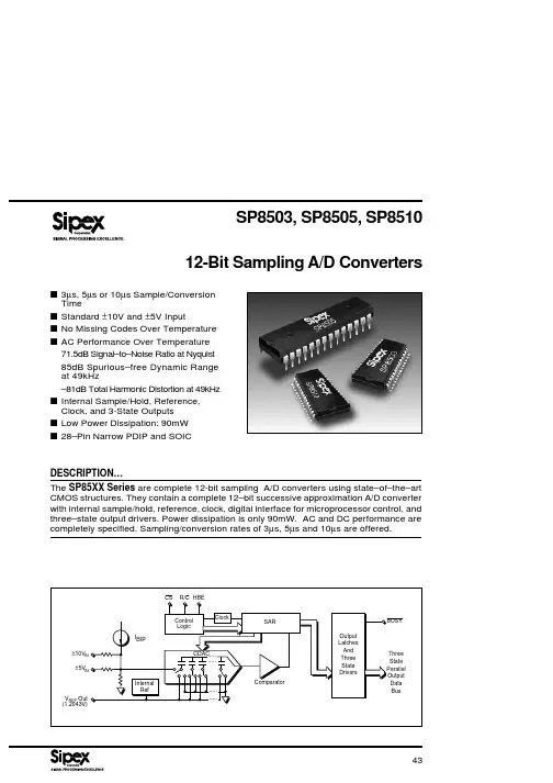
ABSOLUTE MAXIMUM RATINGSThese are stress ratings only and functional operation of the device at these or any other above those indicated in the operation sections of the specifications below is not implied. Exposure to absolute maximum rating conditions for extended periods of time may affect reliability.V S to Digital Common ...............................................................+7V Pin 26 (V SO ) to Pin 27 (V SA )....................................................±0.3V Analog Common to Digital Common......................................±0.3V Control Inputs to Digital Common .......................–0.3 to V S + 0.3 V Analog Input Voltage ...........................................................±16.5V Maximum Junction Temperature ...........................................160°C Internal Power Dissipation ..................................................750mWLead Temperature (soldering, 10s).....................................+300°C Thermal Resistance. ØJA :Plastic DIP .......................................................................50°C/W SOIC ..............................................................................100°C/WSPECIFICATIONSSPECIFICATIONS (continued)NOTES1.LSB means Least Significant Bit. For SP85XX Series, 1LSB =2.44mV for ±5V range, 1 LSB =4.88mV for ±10V range.2.All specifications in dB are referred to a full-scale input, either ±10V or ±5V.3.For full-scale step input, 12-bit accuracy attained in specified time.4.Recovers to specified performance in specified time after 2 x Finput overvoltage.SPINOUTPin 12 — D 5 — Data Bit 5 if HBE is LOW; LOW if HBE is HIGH.Pin 13 — D 4 — Data Bit 4 if HBE is LOW; LOW if HBE is HIGH.Pin 14 —N.C.—This pin is not internally connected.Pin 15 —N.C.—This pin is not internally connected.Pin 16— DGND — Digital Ground. Connect to pin 5, at the device.Pin 17 — D 3 — Data Bit 3 if HBE is LOW; Data Bit 11 if HBE is HIGH.Pin 18 — D 2 — Data Bit 2 if HBE is LOW; Data Bit 10 if HBE is HIGH.Pin 19— D 1 — Data Bit 1 if HBE is LOW; Data Bit 9 if HBE is HIGH.Pin 20 — D 0 — Data Bit 0 if HBE is LOW. Least Significant Bit (LSB). Data Bit 8 if HBE is HIGH.Pin 21 — HBE — High Byte Enable, When held LOW, data output as 12-bits in parallel. When held HIGH, four MSBs presented on pins 17–20, pins 10 – 13 output LOWs. Must be LOW to initiate conversion.Pin 22— R/C — Read/Convert. Falling edge initiates conversion when CS is LOW, HBE is LOW, and BUSY is HIGH.Pin 23 — CS — Chip Select. Outputs in Hi-Z state when HIGH. Must be LOW to initiate conversion or read data.Pin 24 — BUSY. Output LOW during conver-sion. Data valid on rising edge in Convert Mode.Pin 25 — N .C. — T his p in i s n ot i nternally c onnected.Pin 26 — V SD — Positive Digital Power Supply, +5V.Connect to pin 27, and bypass to DGND.Pin 27 — V SA — Positive Analog Power Supply.+5V. Connect to pin 26, and bypass to AGND.Pin 28 — N.C. — This pin is not internally connected.PIN ASSIGNMENTPin 1 —No Connection —This pin is not internally connected.Pin 2 — IN 1 — ±10V Analog Input. Connected to AGND for ±5V range.Pin 3 — IN 2 — ±5V Analog Input. Connected to AGND for ±10V range.Pin 4 — V REF – Internal Voltage. Reference Output.Pin 5 — AGND — Analog Ground. Connect to pin 16 at the device.Pin 6 — D 11 — Data Bit 11. Most Significant Bit (MSB).Pin 7 — D 10 — Data Bit 10.Pin 8— D 9 — Data Bit 9.Pin 9 — D 8 — Data Bit 8.Pin 10 — D 7 — Data Bit 7 if HBE is LOW; LOW if HBE is HIGH.Pin 11 — D 6 — Data Bit 6 if HBE is LOW; LOW if HBE is HIGH.edge can be used to read the data from the conver-sion. Also, during conversion, the BUSY signal puts the output data lines in Hi-Z states and inhibits the input lines. This means that pulses on R/C are ignored, so that new conversions cannot be initi-ated during a conversion, either as a result of spurious signals or to short-cycle the SP85XX Series.In the Read Mode, the input to R/C is kept nor-mally LOW, and a HIGH pulse is used to read data and initiate a conversion. In this mode, the rising edge of R/C will enable the output data pins, and the data from the previous conversion becomes valid. The falling edge then puts the SP85XX Series in a hold mode, and initiates a new conver-sion.The SP85XX Series will begin acquiring a new sample just prior to the BUSY output rising, and will track the input signal until the next conversion is started.For u se w ith a n 8-bit b us, t he d ata c an b e r ead o ut i n t wo bytes under the control of HBE. With a LOW input on HBE, at the end of a conversion, the 8 LSBs of data are loaded into the output drivers on D 7 through D 4 and D 3 through D 0. Taking HBE HIGH then loads the 4MSBs on D 3 through D 0, with D 7 through D 4 being forced LOW.Analog Input RangesThe SP85XX Series offers two standard bipolar input ranges: ±10V and ±5V. If a ±10V range is required, the analog input signal should be con-nected to pin 2. A signal requiring a ±5V range should be connected to pin 3. In either case, the other pin of the two must be grounded or connected to the adjustment circuits described in the section on calibration.Controlling The SP85XX SeriesThe SP85XX Series can be easily interfaced to most microprocessor-based and other digital systems. The microprocessor may take full control of each conver-sion, or the SP85XX Series may operate in a stand-alone mode, controlled only by the R/C input. Full control consists of initiating the conversion and read-ing the output data at user command, transmitting data either all 12-bits in one parallel word, or in two 8-bit bytes. The three control inputs (CS, R/C and HBE) areFEATURES...The SP85XX Series are specified at sampling rates of 333kHz (SP8503), 200kHz (SP8505) or 100kHz (SP8510). Conversion times are factory set for 2.70µs, 4.7µs and 9.7µs maximum, re-spectively, over temperature, and the high-speed sampling input stage insures a total acqui-sition and conversion time of 3µs, 5µs and 10µs maximum, respectively, over temperature. Pre-cision, laser-trimmed scaling resistors provide industry–standard input ranges of ±5V or ±10V.The 28-pin SP85XX Series are available in narrow body plastic DIP, and SOIC packages and it operates from a single +5V supply.The SP85XX Series are available in grades specified over the 0°C to +70°C commercial temperature ranges.OPERATION Basic OperationFigure 1 shows the simple hookup circuit required to operate the SP85XX Series in a ±10V range in the Convert Mode. A convert command arriving SP85XX Series in the HOLD mode, and a conversion is started. This pulse must be LOW for a minimum of 40ns. Because this pulse establishes the sampling instant of the A/D,it must have very low jitter. BUSY will be held LOW during the conversion, and rises only after the conversion is completed and the data has been transferred to the output drivers. Thus, the risingFigure 1. Basic ±10V OperationTable 1. Control Line Functionsin Table 2. No other combination of states or transi-tions w ill i nitiate a c onversion. C onversion i s i nhibited if either CS or HBE are HIGH, or if BUSY is LOW.CS and HBE should be stable a minimum of 25ns prior to the transition on R/C. Timing relationships for start of conversion are illustrated in Figure 7.The BUSY output indicates the current state of the converter by being LOW only during conversion.During this time the three-state output buffers remain in a Hi-Z state, and therefore data cannot be read during conversion. During this period, additional transitions on the three digital inputs (CS, R/C and HBE) will be ignored, so that conversion cannot be prematurely terminated or restarted.Internal ClockThe SP85XX Series has an internal clock that is factory trimmed to achieve the typical conversion times given in the specifications, and a maximum conversion time over the full operating tempera-ture range of 2.7µs, 4.7µs or 9.7µs, depending on the model. No external adjustments are required,and with the guaranteed maximum acquisition time of 300ns, throughput performance is assured with convert pulses as close as 3µs for the SP8503.Reading DataAfter c onversion i s i nitiated, t he o utput b uffers r emain in a Hi-Z state until the following three logic condi-tions are simultaneously met: R/C is HIGH, BUSY is HIGH and CS is LOW. Upon satisfying these condi-tions, the data lines are enabled according to the state of HBE. See Figure 7 for timing relationships and specifications.CALIBRATION...Optional External Gain And Offset Trim Offset and full-scale errors may be trimmed to zero using external offset and full-scale trim potenti-ometers connected to the SP85XX Series as shown in Figure 3.If adjustment of offset and full scale is not required,connections as shown in Figure 2 should be used.all TTL/CMOS compatible. The functions of the control lines are shown in Table 1.For stand-alone operation, control of the SP85XX Series is accomplished by a single control line connected to R/C. In this mode, CS and HBE are connected to GND. The output data are presented as 12-bit words. The stand-alone mode is used in systems containing dedicated input ports which do not require full bus interface capability.Conversion is initiated by a HIGH-to-LOW transition on R /C. T he t hree-state d ata o utput b uffers a re e nabled when R/C is HIGH and BUSY is HIGH. Thus, there are two possible modes of operation: conversion can be initiated with either positive or negative pulses. In either case, the R/C pulse must remain LOW a minimum of 40ns.Figure 5 illustrates timing when conversion is initi-ated by an R/C pulse which goes LOW and returns HIGH during the conversion. In this case (Convert Mode), the three-state outputs go into the Hi-Z state in response to the falling edge of R/C, and are enabled for external access to the data after completion of the conversion.Figure 6 illustrates the timing when conversion is initiated by a positive R/C pulse. In this mode (Read Mode), the output data from the previous conversion is enabled during the HIGH portion of R/C. A new conversion starts on the falling edge of R/C, and the three-state o utputs r eturn t o t he H i-Z s tate u ntil t he n ext occurrence of a HIGH on R/C.Conversion StartA conversion is initiated on the SP85XX Series only by a negative transition occurring on R/C, as shown Figure 2. a) ±10V Range b) ±5V Range — Without TrimsINPUT VOLTAGE RANGE AND LSB VALUESInput Voltage Range Defined As:±10V ±5V Analog Input Connected to Pin 2 3Pin Connected to AGND 32One Least Significant Bit (LSB)FSR/21220V/21210V/2124.88mV2.44mVOUTPUT TRANSITION VALUESFFEH TO FFFH + FULL SCALE +10V–3/2LSB +5V–3/2LSB +9.9927V +4.9963V 7FFH TO 800H Mid Scale 0V–1/2LSB 0V–1/2LSB (Bipolar Zero)–2.44mV –1.22mV 000H to 001H–Full Scale–10V+1/2LSB –5V+1/2LSB -9.9976V-4.9988VTable 2. Input Voltages, Transition Voltages and LSB Valuestoggles on and off at code 1111 1111 1110BIN=FFE H= 4094DEC.±10V Range Offset and GainOffset — Apply 1.2622V to the ±10V input at pin 2. Adjust the offset potentiometer until the LSB toggles on and off at code 1001 00000010BIN= 902H= 2306DEC.Gain — Apply 9.9927V to the ±10V input at pin 2. Adjust the gain potentiometer until the LSB toggles on and off at code 1111 1111 1110BIN=FFE H= 4094DEC.Layout ConsiderationsBecause of the high resolution and linearity of the SP85XX Series , system design problems such as ground path resistance and contact resis-tance become very important.Calibration ProcedureApply a precision input voltage source to your chosen input range (±10V range at pin 2 or ±5V at pin 3). Set the A/D to convert continuously.Monitor the output code. Trim the offset first,then gain. Use the appropriate input voltages and output target codes for your chosen input range as follows. The recommended offset cali-bration voltage values eliminate interaction be-tween the offset and gain calibration±5V Range Offset and GainOffset — Apply 1.5637V to the ±5V input at pin 3. Adjust the offset potentiometer until the LSB toggles on and off at code 1010 1000 0000BIN=A80H= 2688DEC.Gain — Apply 4.9963V to the ±5V input at pin 3. Adjust the gain potentiometer until the LSBFigure 3. a) ±10V Range b) ±5V Range — With External TrimsThe input resistance of the SP85XX Series is 6.3k Ω or 4.2K Ω (for the ±10V and ±5V ranges respectively). To avoid introducing distortion, the source resistance must be very low, or constant with signal level. The output impedance provided by most op amps is ideal. Pins 26 Digital Supply Voltage (V SD ) and 27 Analog Supply Voltage (V SA ) are brought out to separate pins to maximize accuracy on the chip. They should be connected together as close as possible to the unit. Pin 27 may be slightly more sensitive than pin 26 to supply variations, but to maintain maximum system accu-racy, both should be well–isolated from digital supplies with wide load variations.To limit the effects of digital switching elsewhere in a system on the analog performance of the system, it often makes sense to run a separate +5V supply conductor from the supply regulator to any analog components requiring +5V, including the SP85XX Series. If the SP85XX Series traces cannot be separated back to the power supply terminals, and therefore share the same trace as the logic supply currents, then a 10 Ohm isolating resistor should be used between the board supply and pin 24 (V DA ) and its bypass capacitors, to keep V DA glitch–free. The V S pins (26 and 27) should be connected together and bypassed with a parallel combination of a 6.8µF Tantalum capacitor and a 0.1µF ceramic capacitor located close to the con-verter to obtain noise-free operation. (See Figure1). Noise on the power supply lines can degrade converter performance, especially noise and spikes from a switching power supply. Appropriate sup-plies or filters must be used.The GND pins (5 and 16) are also separated internally,and should be directly connected to a ground plane under the converter. A ground plane is usually the best solution for preserving dynamic performance and reducing noise coupling into sensitive converter cir-cuits. Where any compromises must be made, the common return of the analog input signal should be referenced to pin 5, AGND, on the SP85XX Series,which prevents any voltage drops that might occur in the power supply common returns from appearing in series with the input signal.Coupling b etween a nalog i nput a nd d igital l ines s hould be minimized by careful layout. For instance, if the lines must cross, they should do so at right angles.Parallel analog and digital lines should be separated from each other by a pattern connected to common.If external full scale and offset potentiometers are used, the potentiometers and related resistors should be located as close to the SP85XX Series as possible.“Hot Socket” PrecautionTwo separate +5V V S pins, 26 and 27, are used to minimize noise caused by digital transients. If one pin is powered and the other is not, the SP85XXFigure 4. Acquisition and Conversion TimingFigure 5. Convert Mode Timing — R/C Pulse LOW, Outputs Enabled After ConversionSeries may draw excessive current. In normal operation, this is not a problem because both pins will be soldered together. However, during evalu-ation, incoming inspection, repair, etc., where the potential of a “Hot Socket” exists, care should be taken to apply power to the SP85XX Series only after it has been socketed.Minimizing “Glitches”Coupling of external transients into an analog-to-digital converter can cause errors which are difficult to debug. In addition to the discussions earlier on layout considerations f or s upplies, b ypassing a nd g rounding, there are several other useful steps that can be taken to get the best analog performance out of a system using the SP85XX Series. These potential system problem sources are particularly important to consider when developing a new system, and looking for the causes of errors in breadboards.First, care should be taken to avoid glitches during critical times in the sampling and conversion process. Since the SP85XX Series has an internal sample/hold function, the signal that puts it into the hold state (R/C going LOW) is critical, as it would be on any sample/ hold amplifier. The R/C falling edge should have a 5 to 10ns transition time, low jitter, and have minimal ringing, especially during the 20ns after it falls.Figure 6. Read Mode Timing — R/C Pulse HIGH, Outputs Enabled Only When R/C is HighAC DYNAMIC TIMING DATANaturally, transients on the analog input signal are to be avoided, especially at times within ±20ns of R/C going LOW, when they may be trapped as part of the charge on the capacitor array. This requires careful layout of the circuit in front of the SP85XX Series.Finally, in multiplexed systems, the timing relative to when the multiplexer is switched may affect the analog performance of the system. In most applica-tions, the multiplexer can be switched as soon as R/C goes LOW (with appropriate delays), but this may affect the conversion if the switched signal shows glitches or significant ringing at the SP85XX Series input. Whenever possible, it is safer to wait until the conversion is completed before switching and multi-plexer. The extremely fast acquisition time and con-version time of the SP85XX Series make this practi-cal in many applications.Although not normally required, it is also good prac-tice to avoid glitches from coupling to the SP85XX Series while bit decisions are being made. Since the above discussion calls for a fast, clean rise and fall on R/C, it makes sense to keep the rising edge of the convert pulse outside the time when bit decisions are being made. In other words, the convert pulse should either b e s hort (under 100ns s o t hat i t t ransitions b efore the MSB decision), or relatively long (over 2.75µs to transition after the LSB decision).Next, although the data outputs are forced into a Hi-Z state during conversion, fast bus transients can still be capacitively coupled into the SP85XX Series. If the data bus experiences fast transients during conver-sion, these transients can be attenuated by adding a logic buffer to the data outputs. The BUSY output can be used to enable the buffer.SYMBOL/PARAMETER MIN .TYP.MAX.UNITS t W R/C Pulse Width 40ns t DBC BUSY delay from R/C 80150ns t B BUSY LOW 2.47 2.7µs t AP Aperture Delay 13ns ∆t AP Aperture Jitter 150ps, rmst C Conversion Time2.5 2.70µs t DBE BUSY from End of Conversion 100ns t DB BUSY Delay after Data Valid 2575200ns t A Acquisition Time 130300nst A + t CThroughput Time SP8503 3.0µs SP8505 5.0µs SP851010.0µs t HDR Valid Data Held After R/C LOW 2050ns t S CS or HBE LOW before R/C Falls 255ns t H CS or HBE LOW after R/C Falls250ns t DD Data Valid from CS LOW, R/C HIGH, and HBE 65150nsin Desired State (Load = 100pF)t HLDelay to Hi-Z State after R/C Falls or 50150nsCS Rises (3K Ω Pullup or PulldownAll parameters Guaranteed By Design.Figure 7. Conversion Start TimingORDERING INFORMATION0°C to +70°CModel Throughput Package SP8503KN....................................................................333kHz................................................................................................28–pin 0.3" Plastic DIP SP8503KS....................................................................333kHz........................................................................................................28–pin, 0.3" SOIC SP8505KN....................................................................200kHz................................................................................................28–pin 0.3" Plastic DIP SP8505KS....................................................................200kHz........................................................................................................28–pin, 0.3" SOIC SP8510KN....................................................................100kHz................................................................................................28–pin 0.3" Plastic DIP SP8510KS....................................................................100kHz........................................................................................................28–pin, 0.3" SOICTHIS PAGE LEFT INTENTIONALLY BLANK。