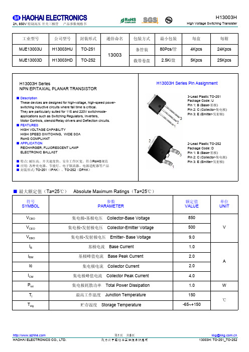
KSE13003 NPN Silicon Transistor
- 格式:pdf
- 大小:28.44 KB
- 文档页数:2

13003三极管参数,中文资料13003三极管在整流器,充电器中很常用,对于了解13003三极管参数也显得很必要,下面为大家提供13003三极管的常用参数及应用电路图。
13003NPN型硅晶体管、功率开关三极管 主要应用于:日光灯、电子镇流器、充电器、等高压功率开关电路。
13003产品特性:芯片面积:1.63×1.63(特制芯片)额定电流:1.5 A(加大电流品种)饱和压降低、热性能好反向击穿电压高、漏电流小N型硅单晶三重扩散平面工艺制作 <<提示: 你觉得本站资料对你有帮助,请将网页加入浏览器收藏夹中,方便以后点击直接访问。
欢迎大家为容源电子网提供技术资料。
》温馨提示:将鼠标指针放在图片上,滚动鼠标可以动态改变图片大小,方便分析电路 型号与封装识别对照:HI13003: TO-251 (直插封装)HJ13003: TO-252 (贴片封装)HMJE13003T: TO-126 (半塑封)HMJE13003D: TO-126ML (全塑封)HMJE13003E: TO-220 (半塑封)你觉得本站资料对你有帮助,请将网页加入浏览器收藏夹中,方便以后点击直接访问。
欢迎大家为容源电子网提供技术资料。
》13003最大额定值温馨提示:将鼠标指针放在图片上,滚动鼠标可以动态改变图片大小,方便分析电路图。
<<提示: 你觉得本站资料对你有帮助,请将网页加入浏览器收藏夹中,方便以后点击直接访问。
欢迎大家为容源电子网提供技术资料。
》13003三极管应用电路图:>> 转载请注明出处并保留链接。
编辑:admin 时间:2014-1TAG标签: 整流器 三极管 芯片 高压 晶体管 镇流器 电路图 555 充电 制作【 复制本文地址及标题 】 【 在本地打印该网页 】 【 我要发表文章 】 【 返回上一页】分享到: QQ空间 新浪微博 开心网 人人网 更多...·上一篇: 应用交流接触器实现逆变器和市电自动切换·下一篇: 格力牌FGW-12远红外电暖器使用注意事项。

npn transistor结构和工作原理一、引言在现代电子技术中,晶体管是一种最为基本且应用广泛的器件之一。
npn晶体管是一种三层结构的双极型晶体管,其结构和工作原理给予它广泛的应用场景。
本文将详细探讨npn transistor的结构和工作原理。
二、结构npn晶体管的结构由两个PN结构构成,其中一个P型材料夹在两个N型材料之间。
下面将详细介绍每个结构的作用和组成。
2.1 发射结发射结(Emitter)是npn晶体管中的第一个结构。
它由一块高掺杂的材料组成,通常是N型硅。
发射结有两个主要作用:•1.收集少数载流子(电子)并注入基区。
•2.为基区注入大量载流子。
发射结的高掺杂使得它具有低电阻,能够提供大量的载流子。
2.2 基区基区(Base)是npn晶体管的第二个结构。
它由一块低掺杂的材料构成,通常是P型硅。
基区的主要作用是控制电子流经过晶体管的能力。
由于基区的掺杂浓度较低,它的电阻较高。
这样,当一个正向电压被施加到基极上时,只有很少量的电子能够通过基区并流向集电区。
2.3 集电结集电结(Collector)是npn晶体管的第三个结构。
它由一块中等掺杂的材料构成,通常是N型硅。
集电结的主要作用是收集通过晶体管的大量电流。
集电结的中等掺杂使得它具有较低的电阻,可以接收到从发射结注入的大量电子。
三、工作原理npn晶体管的工作原理是基于PN结和电流控制的。
下面将详细介绍npn晶体管的工作原理和电流流向。
3.1 放大作用npn晶体管有两个主要的工作模式:放大模式和截止模式。
在放大模式下, npn晶体管可以放大电流和功率。
其放大作用可以通过下面的步骤来解释:1.正向偏置:给发射极提供一个相对较高的电压,并将基极连接到一个较低电压。
这样,发射结和基结之间就形成了正向偏置。
2.空穴注入:因为发射极的正向偏置,导致发射结中注入大量的电子进入基区。
3.电子扩散:在基区,这些电子通过碰撞和热激发的方式扩散到基极。
这里的电子在集电结方向上形成了一个电子流。


Philips Semiconductors Product specificationSilicon Diffused Power Transistor PHE13003AUGENERAL DESCRIPTIONHigh-voltage, high-speed planar-passivated npn power switching transistor in the SOT533 envelope intended for use in high frequency electronic lighting ballast applications, converters and inverters, etc.QUICK REFERENCE DATASYMBOL PARAMETERCONDITIONS TYP.MAX.UNIT V CESM Collector-emitter voltage peak value V BE = 0 V-700V V CBO Collector-Base voltage (open emitter)-700V V CEO Collector-emitter voltage (open base)-400V I C Collector current (DC)- 1.5A I CM Collector current peak value -3A P tot Total power dissipationT mb ≤ 25 ˚C-50W V CEsat Collector-emitter saturation voltage I C = 1.0 A;I B = 0.25 A - 1.0V h FE I C = 1.0 A; V CE = 5 V -25t fiFall time (Inductive)I C = 1.0 A; I BON = 0.2 A-150nsPINNING - SOT533PIN CONFIGURATION SYMBOLLIMITING VALUESLimiting values in accordance with the Absolute Maximum Rating System (IEC 134)SYMBOL PARAMETERCONDITIONS MIN.MAX.UNIT V CESM Collector to emitter voltageV BE = 0 V-700V V CEO Collector to emitter voltage (open base)-400V V CBO Collector to base voltage (open emitter)-700V I C Collector current (DC)- 1.5A I CM Collector current peak value -3A I B Base current (DC)-0.75A I BM Base current peak value - 1.5A P tot Total power dissipation T mb ≤ 25 ˚C-50W T stg Storage temperature -65150˚C T jJunction temperature-150˚CTHERMAL RESISTANCESSYMBOL PARAMETERCONDITIONSTYP.MAX.UNIT R th j-mb Junction to mounting base - 2.5K/W R th j-aJunction to ambientin free air 70-K/WPhilips Semiconductors Product specificationSilicon Diffused Power Transistor PHE13003AUSTATIC CHARACTERISTICST mb = 25 ˚C unless otherwise specified SYMBOL PARAMETERCONDITIONSMIN.TYP.MAX.UNIT I CES ,I CBO Collector cut-off current 1V BE = 0 V; V CE = V CESMmax -- 1.0mA I CES V BE = 0 V; V CE = V CESMmax ;-- 5.0mA T j = 125 ˚CI CEO Collector cut-off current 1V CEO = V CEOMmax (400V)--0.1mA I EBOEmitter cut-off currentV EB = 9 V; I C = 0 A --1mA V CEOsust Collector-emitter sustaining voltage I B = 0 A; I C = 10 mA;400--V L = 25 mHV CEsat Collector-emitter saturation voltage I C = 1.0 A;I B = 0.25 A -- 1.0V V BEsat Base-emitter saturation voltage I C = 1.0 A;I B = 0.25 A -- 1.2Vh FE DC current gainI C = 100mA; V CE = 5 V 8-40h FEI C = 1.0 A; V CE = 5 V5-25DYNAMIC CHARACTERISTICST mb = 25 ˚C unless otherwise specified SYMBOL PARAMETERCONDITIONSTYP.MAX.UNIT Switching times (resistive load)I Con = 1.0 A; I Bon = -I Boff = 0.2 A;R L = 75 ohms; V BB2 = 4V;t on Turn-on time-0.9µs t s Turn-off storage time - 4.0µs t f Turn-off fall time-0.7µs Switching times (inductive load)I Con = 1.0 A; I Bon = 0.2 A; L B = 1 µH;-V BB = 5 Vt s Turn-off storage time -2µs t f Turn-off fall time-100ns Switching times (inductive load)I Con = 1.0 A; I Bon = 0.2 A; L B = 1 µH;-V BB = 5 V; T j = 100 ˚Ct s Turn-off storage time -4µs t fTurn-off fall time-150ns1 Measured with half sine-wave voltage (curve tracer).Philips Semiconductors Product specification Silicon Diffused Power Transistor PHE13003AUPhilips Semiconductors Product specification Silicon Diffused Power Transistor PHE13003AUPhilips Semiconductors Product specification Silicon Diffused Power Transistor PHE13003AUPhilips Semiconductors Product specification Silicon Diffused Power Transistor PHE13003AUMECHANICAL DATAPhilips Semiconductors Product specification Silicon Diffused Power Transistor PHE13003AUDEFINITIONSData sheet statusObjective specification This data sheet contains target or goal specifications for product development. Preliminary specification This data sheet contains preliminary data; supplementary data may be published later. Product specification This data sheet contains final product specifications.Limiting valuesLimiting values are given in accordance with the Absolute Maximum Rating System (IEC 134). Stress above one or more of the limiting values may cause permanent damage to the device. These are stress ratings only and operation of the device at these or at any other conditions above those given in the Characteristics sections ofthis specification is not implied. Exposure to limiting values for extended periods may affect device reliability. Application informationWhere application information is given, it is advisory and does not form part of the specification.© Philips Electronics N.V. 1999All rights are reserved. Reproduction in whole or in part is prohibited without the prior written consent of the copyright owner.The information presented in this document does not form part of any quotation or contract, it is believed to be accurate and reliable and may be changed without notice. No liability will be accepted by the publisher for any consequence of its use. Publication thereof does not convey nor imply any license under patent or other industrial or intellectual property rights.LIFE SUPPORT APPLICATIONSThese products are not designed for use in life support appliances, devices or systems where malfunction of these products can be reasonably expected to result in personal injury. Philips customers using or selling these products for use in such applications do so at their own risk and agree to fully indemnify Philips for any damages resulting from such improper use or sale.。
.TO-251Plastic-Encapsulate Transistors13003TRANSISTOR (NPN)FEATURESpower switching applicationsMAXIMUM RATINGS (TA=25℃unless otherwise noted)Symbol(符号)Parameter(参数名称)Value(额定值)Units(单位)VCBO Collector-Base Voltage (集电极-基极电压)700V VCEO Collector-Emitter Voltage (集电极-发射极电压)480V VEBO Emitter-Base Voltage (发射极-基极电压)9V IC Collector Current -Continuous (集电极电流) 1.0A PC Collector Power Dissipation (耗散功率)0.9W Tj Junction Temperature (结温)150℃TstgStorage Temperature (储存温度)-55-150℃ELECTRICAL CHARACTERISTICS (Tamb=25℃unless otherwise specified)Parameter (参数名称)Symbol (符号)Test conditions (测试条件)MIN(最小值)TYP (典型值)MAX (最大值)UNIT (单位)Collector-base breakdown voltage 集电极-基极击穿电压V(BR)CBO IC=100μA,IE=0700V Collector-emitter breakdown voltage 集电极-发射极击穿电压V(BR)CEO IC=1mA,IB=0480V Emitter-base breakdown voltage 发射极-基极击穿电压V(BR)EBO IE=100μA,IC=09V Collector cut-off current 集电极-基极截止电流ICBO VCB=600V ,IE=01μA Collector cut-off current 集电极-发射极截止电流ICEO VCE=400V ,IB=010μA Emitter cut-off current 发射极-基极截止电流IEBO VEB=9V ,IC=01μADC current gain 直流电流增益hFE VCE=10V,IC=100mA 830DC current gain 直流电流增益hFE VCE=5V,IC=1mA 8Collector-emitter saturation voltage 集电极-发射极饱和压降VCE(sat)IC=200mA,IB=40mA 0.5V Base-emitter saturation voltage 发射极-基极饱和压降VBE(sat)IC=200mA,IB=40mA1.2VCLASSIFICATION OF hFERange8-1515-2020-2525-30Typical Characteristics 13003I C , C o l l e c t o r C u r r e n t ( A )h F E - I Ch F E , D C C ur r e n t G a i nV C E sat - I CI c , C o l l e c t o r C u r r e n t ( A )V C E s a t (V ),C o l l e c t o r E m i t t e r S a t u r a t i o n V o l t a g eV B E s a t - I CI c , C o l l e c t o r C u r r e n t ( A )V B E s a t (V ), B a s e E m i t t e r S a t u r a t i o n V o l t a g e。
HIGH VOLTAGE FAST-SWITCHINGNPN POWER TRANSISTER Application2005.021/6Electrical charactristics(Tc=25℃)Item Symbol Testing term Min Max UnitsCollector-emitter breakdown voltage V(BR)CEO Ic=10mA,I B=0400 VCollector-base breakdown voltage V(BR)CBO Ic=1mA,I B=0600 VEmitter-base breakdown voltage V(BR)EBO I E=1mA,Ic=09 VCollector-base Cutoff current I CBO V CB=580V, I E=05 μACollector-emitter Cutoff current I CEO V CE=390V,I B=010 μAEmitter-base Cutoff current I EBO V EB=7V, I C=05 μADC current gain hFE V CE=10V, I C=100mA 8 40Collector-emitter Saturation voltage V CE(sat)(1)I C=0.5A, I B=0.1A0.8 VBase-emitter Saturation voltage V BE(sat)I C=0.5A, I B=0.1A1.2 VFall time t f V CC=24V I C=0.25A,I B1=-I B2=0.05A0.7μSStorage time ts V CC=24V I C=0.25A,I B1=-I B2=0.05A4μSTransition frequency f T V CE=10V, Ic=0.1A 4 - MHzThermal charactristicsItem Symbol Min Max UnitsThermal resistance Junction to case R th(j-c)6.25℃/W2005.022/6Typical characteristics:Base-emitter saturation voltage2005.023/62005.024/6NOTES1. Jilin Sino-microelectronics co., Ltd sales its product either through direct sales or salesagent , thus, for customers, when ordering , please check with our company.2. We strongly recommend customers check carefully on the trademark when buying ourproduct, if there is any question, please don’t be hesitate to contact us.3. Please do not exceed the absolute maximum ratings of the device when circuitdesigning.4. Please do not exceed the absolute maximum ratings of the device when circuitdesigning.5. Jilin Sino-microelectronics co, Ltd reserves the right to make changes in thisspecification sheet and is subject to change without prior notice.CONTACTJilin Sino-Microelectronics Co.,LtdAdd:No.99 Shenzhen Street,Jilin City Jilin Province ChinaZip:132013Tel:86-432-4678411Fax:(0432)4665812Web:Marking DepartmentJilin City:Add:No.99 Shenzhen Street,Jilin City Jilin Provine ChinaTel: (0432)4675588 4675688 (0432)4678411-3098\3099Fax: (0432)46715332005.025/6。
NPN SILICON POWER TRANSISTORCDT13003 TO-220Plastic PackageApplicationsSuitable for Lighting, Switching Regulator and Motor ControlABSOLUTE MAXIMUM RATINGS DESCRIPTIONSYMBOL Collector Base Voltage V CBOCollector Emitter (sus) Voltage V CEO Emitter Base VoltageV EBO Collector Current Continuous I C Peak (1)I CM Base Current Continuous I B Peak (1)I BM Emitter Current ContinuousI E Peak (1)I EM Power Dissipation @ T a =25 ºC P DDerate Above 25ºCPower Dissipation @ T c=25 ºC P D Derate Above 25ºCOperating And Storage Junction Temperature Range T j, T stgTHERMAL RESISTANCE Junction to Case R th (j-c)Junction to AmbientR th (j-a)Maximum Lead Temperature for Soldering Purpose: 1/8" from Case for 5 Seconds(1) Pulse Test: Pulse Width=5ms, Duty Cycle=10%ELECTRICAL CHARACTERISTICS (T a =25ºC unless specified otherwise)DESCRIPTIONSYMBOL TEST CONDITIONMIN TYP MAX UNIT Collector Base Voltage V CBO I C =1mA, I E =0600--V Collector Emitter (sus) Voltage *V CEO(sus)I C =10mA, I B =0400--V Collector Cut Off Current I CBO V CB =600V , I E =0-- 1.0mA V CB =600V , I E =0, T c =100ºC5.0mA Emitter Cut Off CurrentI EBOV EB =9V, I C =0--1.0mA*Pulse Test:- PW=300µs, Duty Cycle=2%CDT13003Rev_1 230306D275ºCT LUNIT V V V A A A W A A A ºCºC/W ºC/W VALUE 6004009.01.83.50.751.5 - 65 to+1502.08892.254.51.411.2mW/ ºC W mW/ ºC 50480Continental Device India LimitedAn ISO/TS 16949, ISO 9001 and ISO 14001 Certified CompanyNPN SILICON POWER TRANSISTORCDT13003 TO-220Plastic PackageELECTRICAL CHARACTERISTICS (T a =25ºC unless specified otherwise)DESCRIPTION SYMBOL TEST CONDITION MIN TYP MAX UNITDC Current Gain*h FE **I C =0.5A, V CE =5V 11 - 30I C =1.5A, V CE =5V4-25Collector Emitter Saturation Voltage*V CE (sat)I C =0.5A, I B =0.1A --0.5V I C =1A, I B =0.25A -- 1.0V I C =1.5A, I B =0.5A -- 2.5V I C =1A, I B =0.25A,T c =100ºC-- 1.0V Base Emitter Saturation Voltage*V BE (sat)I C =0.5A, I B =0.1A -- 1.0V I C =1A, I B =0.25A -- 1.2V I C =1A, I B =0.25A,T c =100ºC-- 1.1V DYNAMIC CHARACTERISTICS DESCRIPTIONSYMBOLTEST CONDITION MIN TYP MAX UNIT Current Gain Bandwidth Product f T I C =100mA, V CE =10V,f=1MHz4.0--MHz Output Capacitance C obV CB =10V, f=0.1MHz-21-pFSWITCHING TIME Turn On Time t on 1.1µs Storage Time t stg 4.0µs Fall Timet f0.7µs** h FE Classification:-Note:- Product is pre selected in DC current A B C E F gain (Groups A to F). CDIL reserves the right11-16 15-19 18-22 21-25 24-30to ship any of the groups according to production availability.MARKINGCDT CDT CDT CDT CDT 13003 13003 13003 13003 13003 A XY B XY C XY E XY F XYX= Year of Manufacturer Code Y= Month Code*Pulse Test:- PW=300µs, Duty Cycle=2%CDT13003Rev_1 230306DV CC =125V, I C =1A, I B1=0.2A,I B2=0.2ACDT13003 TO-220Plastic PackageCDT13003Rev_1 230306DTO-220 Plastic PackageTO-220 Tube PackingTO-220 / FP200 pcs/polybag 50 pcs/tube 396 g m /200 pcs 120 gm /50 pcs3" x 7.5" x 7.5"3.5" x 3.7" x 21.5"1.0K 1.0K17" x 15" x 13.5"19" x 19" x 19"16.0K 10.0K36 k g s 29 k g sPACKAGENet Weight/Q t yDetailsSTANDARD PACKINNER CARTON BOXQ t y OUTER CARTON BOXQ t y G r W t SizeSizePacking DetailPin Configuration 1. Base 2. Collector 3. Emitter 4. CollectorComponent Disposal Instructions1. CDIL Semiconductor Devices are RoHS compliant, customers are requested to please dispose as per prevailing Environmental Legislation of their Country.CDT13003Rev_1 230306DCustomer NotesDisclaimerThe product information and the selection guides facilitate selection of the CDIL's Semiconductor Device(s)best suited for application in your product(s)as per your requirement.It is recommended that you completely review our Data Sheet(s)so as to confirm that the Device(s)meet functionality parameters for your application.The information furnished in the Data Sheet and on the CDIL Web Site/CD are believed to be accurate and reliable.CDIL however,does not assume responsibility for inaccuracies or incomplete information.Furthermore,CDIL does not assume liability whatsoever,arising out of the application or use of any CDIL product;neither does it convey any license under its patent rights nor rights of others.These products are not designed for use in life saving/support appliances or systems.CDILcustomerssellingtheseproducts(eitherasindividualSemiconductorDevicesorincorporatedintheirendproducts),in any life saving/support appliances or systems or applications do so at their own risk and CDIL will not be responsible for any damages resulting from such sale(s).CDIL strives for continuous improvement and reserves the right to change the specifications of its products without prior notice.CDIL is a registered Trademark of Continental Device India LimitedC-120 Naraina Industrial Area, New Delhi 110 028, India.Telephone + 91-11-2579 6150, 4141 1112 Fax + 91-11-2579 5290, 4141 1119email@ Continental Device India Limited Data Sheet Page 4 of 42. In Europe, please dispose as per EU Directive 2002/96/EC on Waste Electrical and Electronic Equipment (WEEE).TO-220CDT13003Plastic Package元器件交易网。
KSE13003 NPN SILICON TRANSISTOR
HIGH VOLTAGE SWITCH MODE APPLICATIONS
• High Speed Switching
• Suitable for Switching Regulator and Motor Control
ABSOLUTE MAXIMUM RATINGS
ELECTRICAL CHARACTERISTICS (Tc=25&)
%
Pulse Test : Pulse Width=5ms, Duty Cycle 10%
Characteristic
Symbol Rating Unit Collector-Base Voltage Collector-Emitter Voltage Emitter-Base Voltage Collector Current (DC) Collector Current (Pulse) Base Current
Collector Dissipation (T C =25&) Junction Temperature Storage Temperature
V CBO V CEO V EBO I C I C I B P C T J T STG
700400 91.5 30.75 20150-65 ~ 150
V V V A A A W &&
Characteristic
Symbol Test Condition Min Typ Max Unit %
Collector- Base Breakdown Voltage Emitter- Base Breakdown Voltage
%
DC Current Gain
%
Collector Emitter Saturation Voltage
%
Base Emitter Saturation Voltage Output Capacitance
Current Gain Bandwidth Product Turn On Time Storage Time Fall Time
V CEO (sus) I EBO h FE V CE (sat)
V BE (sat) C OB f T t ON t STG t F
I C = 5mA, I B = 0 V EB = 9V, I C = 0 V CE = 2V, I C = 0.5A V CE = 2V, I C =1A I C = 0.5A, I B = 0.1A I C = 1A, I B = 0.25A I C = 1.5A, I B = 0.5A
I C = 0.5A, I B = 0.1A I C = 1A, I B = 0.25A V CB = 10V , f = 0.1MHz V CE = 10V, I C = 0.1A V CC =125V, I C = 1A
I B1 = 0.2A, I B2 = -0.2A
400
8 5
4
21
10
400.5 1 3 11.2
1.14.00.7
V uA
V V V V V pF MHz
uS uS uS
1 . Emitter 2. Collector 3. Base
TO-126
©1999 Fairchild Semiconductor Corporation
Rev. B
TRADEMARKS
ACEx™CoolFET™
CROSSVOLT™E 2CMOS TM FACT™
FACT Quiet Series™FAST ®FASTr™GTO™HiSeC™
The following are registered and unregistered trademarks Fairchild Semiconductor owns or is authorized to use and is not intended to be an exhaustive list of all such trademarks.
LIFE SUPPORT POLICY
FAIRCHILD’S PRODUCTS ARE NOT AUTHORIZED FOR USE AS CRITICAL COMPONENTS IN LIFE SUPPORT
DEVICES OR SYSTEMS WITHOUT THE EXPRESS WRITTEN APPROV AL OF FAIRCHILD SEMICONDUCTOR CORPORA TION.As used herein:
ISOPLANAR™MICROWIRE™POP™
PowerTrench™QS™
Quiet Series™SuperSOT™-3SuperSOT™-6SuperSOT™-8TinyLogic™
1. Life support devices or systems are devices or systems which, (a) are intended for surgical implant into
the body, or (b) support or sustain life, or (c) whose
failure to perform when properly used in accordance
with instructions for use provided in the labeling, can be reasonably expected to result in significant injury to the user.
2. A critical component is any component of a life
support device or system whose failure to perform can be reasonably expected to cause the failure of the life support device or system, or to affect its safety or effectiveness.PRODUCT STATUS DEFINITIONS Definition of Terms Datasheet Identification Product Status Definition
Advance Information
Preliminary No Identification Needed Obsolete This datasheet contains the design specifications for product development. Specifications may change in any manner without notice.
This datasheet contains preliminary data, and
supplementary data will be published at a later date.Fairchild Semiconductor reserves the right to make changes at any time without notice in order to improve design.
This datasheet contains final specifications. Fairchild Semiconductor reserves the right to make changes at any time without notice in order to improve design.
This datasheet contains specifications on a product that has been discontinued by Fairchild semiconductor.The datasheet is printed for reference information only.
Formative or In Design
First Production
Full Production
Not In Production
DISCLAIMER
FAIRCHILD SEMICONDUCTOR RESERVES THE RIGHT TO MAKE CHANGES WITHOUT FURTHER NOTICE TO ANY PRODUCTS HEREIN TO IMPROVE RELIABILITY , FUNCTION OR DESIGN. FAIRCHILD DOES NOT ASSUME ANY LIABILITY ARISING OUT OF THE APPLICATION OR USE OF ANY PRODUCT OR CIRCUIT DESCRIBED HEREIN; NEITHER DOES IT CONVEY ANY LICENSE UNDER ITS PATENT RIGHTS, NOR THE RIGHTS OF OTHERS.
UHC™VCX™。