Improving Clock Synchronization for MPEG-2 Services over ATM Networks
- 格式:pdf
- 大小:301.34 KB
- 文档页数:11
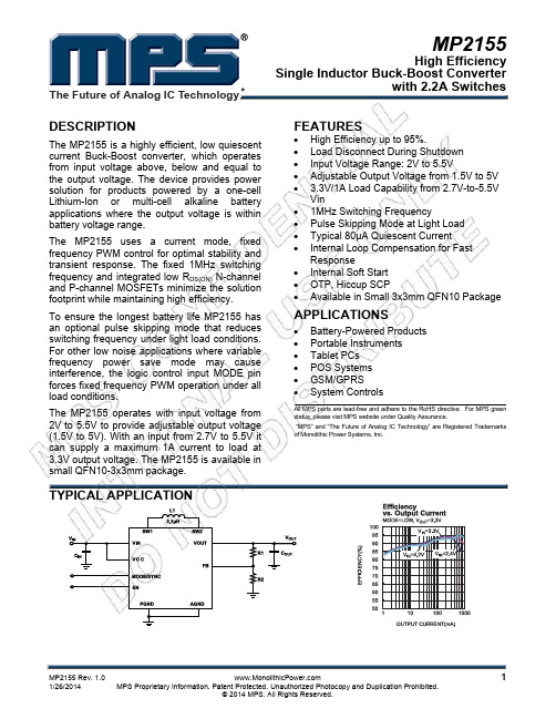
MP2155HighEfficiencySingle Inductor Buck-Boost Converterwith 2.2A SwitchesThe Future of Analog IC TechnologyDESCRIPTIONThe MP2155 is a highly efficient, low quiescent current Buck-Boost converter, which operates from input voltage above, below and equal to the output voltage. The device provides power solution for products powered by a one-cell Lithium-Ion or multi-cell alkaline battery applications where the output voltage is within battery voltage range.The MP2155 uses a current mode, fixed frequency PWM control for optimal stability and transient response. The fixed 1MHz switching frequency and integrated low R DS(ON) N-channel and P-channel MOSFETs minimize the solution footprint while maintaining high efficiency.To ensure the longest battery life MP2155 has an optional pulse skipping mode that reduces switching frequency under light load conditions. For other low noise applications where variable frequency power save mode may cause interference, the logic control input MODE pin forces fixed frequency PWM operation under all load conditions.The MP2155 operates with input voltage from 2V to 5.5V to provide adjustable output voltage (1.5V to 5V). With an input from 2.7V to 5.5V it can supply a maximum 1A current to load at 3.3V output voltage. The MP2155 is available in small QFN10-3x3mm package. FEATURES•High Efficiency up to 95%.•Load Disconnect During Shutdown•Input Voltage Range: 2V to 5.5V •Adjustable Output Voltage from 1.5V to 5V • 3.3V/1A Load Capability from 2.7V-to-5.5V Vin•1MHz Switching Frequency•Pulse Skipping Mode at Light Load• Typical 80μA Quiescent Current •Internal Loop Compensation for Fast Response•Internal Soft Start•OTP, Hiccup SCP•Available in Small 3x3mm QFN10 Package APPLICATIONS• Battery-Powered Products•Portable Instruments•Tablet PCs• POS Systems• GSM/GPRS• System ControlsAll MPS parts are lead-free and adhere to the RoHS directive. For MPS green status, please visit MPS website under Quality Assurance.“MPS” and “The Future of Analog IC Technology” are Registered Trademarks of Monolithic Power Systems, Inc.TYPICAL APPLICATIONORDERING INFORMATIONPart Number* Package Top Marking MP2155GQ* QFN10 (3X3) ADR* For Tape & Reel, add suffix –Z (e.g. MP2155GQ–Z);PACKAGE REFERENCETOP VIEW11065M O DE/SYNC VCC ENA G NDFBSW 1PG ND VINSW 2VO UT 234789EPABSOLUTE MAXIMUM RATINGS (1)IN to GND.....................................–0.3V to 6.5VSW1/2 to GND......–0.3V(-2V for <10ns) to 6.5V All Other Pins...............................–0.3V to 6.5 V Junction Temperature...............................150°C Lead Temperature....................................260°CContinuous Power Dissipation (T A = +25°C)(3)QFN10 3X3mm..........................................2.5W Storage Temperature...............-65°C to +150°CRecommended Operating Conditions (4)Supply Voltage V IN .............................2V to 5.5V Output Voltage V OUT ...........................1.5V to 5V Operating Junct. Temp. (T J )....–40°C to +125°CThermal Resistance (5)θJA θJC3X3 QFN10.............................50......12...°C/WNotes:1) Exceeding these ratings may damage the device2) The maximum allowable power dissipation is a function of themaximum junction temperature T J (MAX), the junction-to-ambient thermal resistance θJA , and the ambient temperature T A . The maximum allowable continuous power dissipation at any ambient temperature is calculated by P D (MAX) = (T J (MAX)-T A )/θJA . Exceeding the maximum allowable power dissipation will cause excessive die temperature, and the regulator will go into thermal shutdown. Internal thermal shutdown circuitry protects the device from permanent damage.3) The device is not guaranteed to function outside of itsoperating conditions.4) Measured on JESD51-7, 4-layer PCB.ELECTRICAL CHARACTERISTICSV IN = V CC =V EN =3.3V, T J = 25°C, unless otherwise noted.Parameter Symbol Condition Min Typ Max Units V CC rising 1.8 1.9 V Under voltage lockout thresholdV UVLOV CC falling1.60VFeedback voltage V FB486 496 506 mV Oscillator frequency90010001300kHzFrequency range forsynchronization F REQ 1000 2000 kHzPrimary current limit 1.8 2.2 ASecondary current limit Isw1.8 A NMOS switch on resistance R DS(ON)-N 105 m Ω PMOS switch on resistance R DS(ON)-P 120 m Ω Quiescent current I Q V FB =0.65V 80 μA Shutdown current I S V EN =0V 1 μA MODE input low voltage 0.4 V MODE input high voltage 1.2 V EN input low voltage 0.4 V EN input high voltage 1.2 VV EN = 3.3V 3.1 μAEN input current I ENV EN =0V 0 μA Thermal shutdown (5)T SHDN 160 ℃ Thermal shutdown hysteresis (5)T HYS20℃Notes:5) Guaranteed by engineering sample Characterization, not tested in production.TYPICAL CHARACTERISTICSV IN = 3.3V, V OUT = 3.3V, L = 3.3µH, C OUT=2x22uF, T A = +25ºC, unless otherwise noted.TYPICAL PERFORMANCE CHARACTERISTICSV IN = 3.3V, V OUT = 3.3V, L = 3.3µH, C OUT=2x22uF, T A = +25ºC, unless otherwise noted.TYPICAL PERFORMANCE CHARACTERISTICS (continued)V IN = 3.3V, V OUT = 3.3V, L = 3.3µH, C OUT=2x22uF, T A = +25ºC, unless otherwise noted.Notes:6) Tested with 1.8A inductor peak current at 3.3V input point. Under other V IN conditions, it takes the same current limit variation trend withV IN into consideration as “Current Limit vs. Input Voltage” curve shows"TYPICAL PERFORMANCE CHARACTERISTICS (continued)V IN = 3.3V, V OUT = 3.3V, L = 3.3µH, C OUT=2x22uF, T A = +25ºC, unless otherwise noted.V IN = 3.3V, V OUT = 3.3V, L = 3.3µH, C OUT=2x22uF, T A = +25ºC, unless otherwise noted.V IN = 3.3V, V OUT = 3.3V, L = 3.3µH, C OUT=2x22uF, T A = +25ºC, unless otherwise noted.V IN = 3.3V, V OUT = 3.3V, L = 3.3µH, C OUT=2x22uF, T A = +25ºC, unless otherwise noted.PIN FUNCTIONSPin # Name Description1VOUT Buck-Boost converter output.2 SW2Switch pin-Internal switches are connected to this pin. Connect inductor between SW1 andSW2.3 PGND Power ground.4 SW1Switch pin-Internal switches are connected to this pin. Connect inductor between SW1 andSW2.5 VIN Supply voltage for power stage.6 EN ON/OFF control, it’s not recommended to leave this pin float.7 MODE/SYNCOperation mode selection. If MODE pin is low, the MP2155 automatically switches between PSM and fixed frequency PWM according to the load level. If MODE pin is pulled high, theMP2155 works always in PWM mode.External clock can be applied to MODE pin for changing switching frequency. This pin is sensitive to noise, so it should be strongly pulled up above 1.2V or pulled down below 0.4V. Must NOT leave it float.8 VCC Supply voltage for control stage. 9 AGND Signal ground, should be connected to PGND externally.10 FBFeedback to set output voltage. Keeps this pin and associated trace far from noise sourcelike SW.- EP Thermal pad, which is recommended to connected to PGND.Level shiftVc-BoostBuck -Boost Control logicBuck ComparatorCurrent senseBoost Comparator EAFBVc-BuckSWASWBSWCVOUTSW1SW 2Gate driversCurrent senseReverse ComparatorVoltage ReferenceENVINPGNDPSM ControlMODE /SYNCSlope GeneratorOscillatorVCC AGNDSW DINPUTOUTPUTCinCoutLSS CapFigure 1— Function Block DiagramOPERATIONThe MP2155 is a high efficiency, dual mode buck-boost converter that provides output voltage above, equal to or below the input voltage. When the MODE pin is held high, the MP2155 operates in constant-frequency PWM mode with peak current mode control. As shown in Figure 1, the output voltage is sensed via the FB pin through an external resistor-divider from the output to ground. The voltage difference between FB pin and the internal reference is amplified by error amplifier to generate control signal V C-Buck . By comparing V C-Buck with internal compensation ramp (the sensed SWA’s current with slope compensation) through Buck comparator, a PWM control signal for PWM buck mode is outputted. Another control signal V C-Boost is derived from V C-Buck through level shift. Similarly, V C-Boost compares with the same ramp signal through Boost comparator and generates the PWM control signal for PWM boost mode. The switch topology for the buck-boost converter is shown in Figure 2.SWA SWBSWC SW1SW2SWDVinVoutMP2155Figure 2—Buck-Boost Switch TopologyBuck Region (Vin > Vout)When the input voltage is significantly greater than output voltage, which means the converter can deliver energy to load within the maximum duty cycle of SWA, so the converter operates in buck mode. The control signal V C-Boost is always lower than compensation ramp because Buck can deliver enough energy to load, thus switch D turns on constantly and switch C remains off. Meanwhile, V C-Buck compares with compensation ramp normally and generates PWM signal, therefore, switches A and B are pulse-width-modulated to produce the required duty cycle to support the output voltage.Buck-Boost Region (Vin ≈ Vout)When Vin is close to Vout, due to duty cycle limit of SWA the converter isn’t able to provide wanted energy to load. In this case SWA will be turned on over all the period, that is, there is no BD operation(SWB and SWD being turned on simultaneously). Now a new period begins. Since there is no BD in last period, an offset voltage is added to the ramp signal to make the ramp signal easily hit V C-Buck . At the same time due to loop regulation V C-Boost (as well as V C-Buck ) rises to some level, so that the ramp signal can intersect it to produce the PWM driving signal for Boost operation. After SWC is turned off the ramp signal continues rising (the actual inductor current may rise or fall depending on the difference between Vin and Vout), when the ramp intersects V C-Buck , PWM signal for Buck operation then is generated. Now the buck’s duty cycle is within its limit, so there is BD operation in current period, which means next period the offset voltage will be removed. This is the so-called buck-boost region. With heavy load due to voltage drop on switches the actual input range for this region may be a little wide.Boost Region (Vin < Vout)When the input voltage is significantly lower than output voltage, the converter operates in boost mode. The control signal V C-Buck is always higher than compensation ramp even with the offset voltage always added, thus switch A turns on continuously and switch B remains off. Meanwhile, V C-Boost compares compensation ramp normally and generates PWM signal, therefore, switches C and D are pulse-width-modulated to produce the required duty cycle to support the output regulation voltage.PSMWhen Mode Pin is pulled down below the low level threshold, the MP2155 will automatically enter PSM if load is light. When working in PSM, a train of SW pulses are initiated by a Boost operation, and ended with BD operation. During this process, SWD will be turned off if inductor current is below about 100mA. In actualwaveforms the current may be much lower than this value when SWD is turned off because of internal delay.SCP/OCP vs. two current limitsThere are two current limits in MP2155. The primary one is for steady PWM operation and it’s typically from 2A to 3A, depending on Vin; The secondary one is for limiting inrush current at startup, it’s typically 1.6A to 1.9A, depending on Vin, too. When load is over heavy, the primary limit would protect MP2155 from being over thermal. Therefore Vout would drop due to OCP. If Vout drops below 0.6 times normal output, a hiccup period is initiated to protect MP2155. this is the SCP. In hiccup period, SWA and SWC are turned off while SWB and SWD are turned on. After the hiccup period ends, a soft re-startup begins. Because Vout is below 1V (due to over load or output short), the secondary current takes charge of this process. After Vo rises above 1V, primary current limit get in charge of. Now if load is still over heavy (or output short still exists) such that after SS ends Vout is still below 0.6*V OUT_NORMAL and current hits one of the limits, another hiccup period begins. However if the load recovers to normal value during re-startup so that current doesn’t hit its limit, or, Vout already rises above 0.6*V OUT_NORMAL, the re-startup succeeds, and MP2155 enter normal operation.As to the input/EN startup, the cases are same as the SCP recovery process. EnableThe MP2155 has a dedicated enable control pin (EN). The device operates when it is set high. If it is set low the device stops switching, all the internal blocks are turned off. Tie EN to Vin through a resistor for automatic start up. Due to EN bias or leakage current, the value of this resistor should be set to provide EN pin with a current above 10uA. Any signal to drive this pin should be limited to 100uA if the maximum voltage of this signal is above 6.5V.Internal Soft-startWhen EN pin is pulled high, and at the same time the voltage on Vcc pin is above its UVLO rising threshold MP2155 will start up with Soft-start function to eliminate output overshoot. Soft-start also functions during SCP recovery.Under-Voltage LockoutThe under voltage lockout (UVLO) is implement to protect the device from improper operating at insufficient supply voltage. When the supply voltage at VCC is below the UVLO threshold the device is in shutdown mode. The UVLO rising threshold is about 1.8V with 200mV hysteresis. Over-Temperature ProtectionAn internal temperature sensor continuously monitors the IC junction temperature. If the IC temperature exceeds 160ºC typically the device stops operating. As soon as the temperature falls below 140ºC typically normal operation is restored.APPLICATION INFORMATIONSetting the Output VoltageTo use MP2155 correctly, A resistor divider must be connected between Vout and GND, and the middle point of the divider connected to FB pin as shown in Typically Application on page 1.2R )1V V(1R FBOUT ×−= (1)High R2 resistance (eg. 100k Ω) can reduce the power consumption, while lower than 1M Ω resistance is recommended for R1 for good output accuracy.Inductor SelectionThe inductor is the key passive component for switching converters. With a buck-boost device, the inductor selection affects the boundary conditions in which the converter works, as buck at the maximum input voltage and as a boost at the minimum input voltage.Two critical inductance values are then obtained according to the following formulas. LREQ )MAX (IN OUT )MAX (IN OUT BUCK MIN I F V )V V (V L Δ××−×=−(2)LREQ OUT )MIN (IN OUT )MIN (IN BOOST MIN I F V )V V (V L Δ××−×=− (3)Where:F REQ : minimum switching frequency∆I L : the peak-to-peak inductor ripple inductor current. As a rule of thumb, the peak-to-peak ripple can be set at 10%-20% of the output current.The minimum inductor value for the application is the higher one between Equation 2 and Equation 3. In addition to the inductance value the maximum current the inductor can handle must be calculated in order to avoid saturation. L F V 2)V V (V I I REQ )MAX (IN OUT )MAX (IN OUT OUT BUCK PEAK ×××−×+η=−(4)L F V )V V (V V I V I REQ OUT )MIN (IN OUT )MIN (IN )MIN (IN OUT OUT BOOST PEAK ××−×+×η×=−(5) Where η is the estimated efficiency of MP2155. The maximum of the two values above must be considered when selecting the inductor.Input and Output Capacitor SelectionIt is recommended to use ceramic capacitors with low ESR as input and output capacitors in order to filter any disturbance present in the input line and to obtain stable operation.Minimum values of 10uF for both capacitors are needed to achieve good behavior of the device. The input capacitor must be placed as close as possible to the device.Other ConsiderationMP2155 employs the classic hiccup mode for SCP. This method has an inherited drawback: if the output short is released at a time closed to SS end, then Vo would has overshoot. To attenuate Vo overshoot at SCP recovery, a forward RC series can be connected in parallel with high side resistor of FB divider, as R3 and C5 in Figure 5 shows. The RC acts as a soft startup when Vo short is released at the time of internal SS’s end.PCB Layout Guide1. Input and output capacitors should be close to MP2155’s Vin, Vout and PGND pins.2. The wire connecting input capacitor to Vcc pin should be as short as possible. For better performance in noisy environment, an additional capacitor very close to Vcc pin can be used to bypass noise for Vcc.3. FB resistor divider should be very close to FB pin, and keep FB trace far away from noise.Figure 3 shows an example of PCB layout for which the reference schematic is shown on Figure 4.CinCout L1R1R2ENMODETop LayerL1Bottom Layer Figure 3—PCB LayoutMP 2155S W 14S W 22VIN5Vcc8VOUT1FB10MODE /SYNC7EN6P G N D3A G N D9U1CinCoutCout GNDR 2R 1GNDGNDVINGNDVOUTGNDFigure 4—Reference Circuit for PCB GuideDesign ExampleBelow is a design example following the application guidelines for the specifications:Table 1: Design ExampleV IN (V) 2-5.5 V OUT (V) 3.3VThe detailed application schematic is shown in Figure 5 and its performance can be found in TPC section.TYPICAL APPLICATION CIRCUITSMP2155S W 14S W 22VIN5Vcc8VOUT1FB10MODE/SYNC7EN6P G N D3A G N D9U13.3uHL1NS C110uF/6.3V C222uF 10V C322uF 10V C4231JP1231JP2GND GND 143kR2820kR1GNDGND VIN=2-5.5VGNDGNDR3750k C568pFVOUT=3.3VFigure 5—3.3V Output Application CircuitMP2155S W 14S W 22VIN5Vcc8VOUT1FB10MODE/SYNC7EN6P G N D3A G N D9U13.3uHL1NS C110uF/6.3V C222uF 10V C322uF 10V C4231JP1231JP2GND GND 91kR2820kR1GNDGND VIN=2-5.5VGNDGNDR3681k C522pFVOUT=5VFigure 6—5V Output Application CircuitNOTICE: The information in this document is subject to change without notice. Please contact MPS for current specifications.Users should warrant and guarantee that third party Intellectual Property rights are not infringed upon when integrating MPS products into any application. MPS will not assume any legal responsibility for any said applications.PACKAGE INFORMATIONQFN10 (3mmX3mm)SIDE VIEW TOP VIEW 11065BOTTOM VIEW2.903.101.451.752.903.102.252.550.50BSC0.180.300.801.000.000.050.20 REFPIN 1 ID MARKING1.700.500.25RECOMMENDED LAND PATTERN2.90NOTE:1) ALL DIMENSIONS ARE IN MILLIMETERS .2) EXPOSED PADDLE SIZE DOES NOT INCLUDE MOLD FLASH . 3) LEAD COPLANARITY SHALL BE 0.10 MILLIMETER MAX . 4) DRAWING CONFORMS TO JEDEC MO -229, VARIATION VEED-5. 5) DRAWING IS NOT TO SCALE .PIN 1 IDSEE DETAIL A 2.500.70PIN 1 ID OPTION B R0.20 TYP.PIN 1 ID OPTION A R0.20 TYP.DETAIL A0.300.50PIN 1 IDINDEX AREA。

Value Engineering0引言在我国军事和航天领域中,导航定位和授时系统在北斗信息服务中占据着越来越重要的地位。
而时钟同步是精密授时的根本保证[1]。
铷钟短期稳定度较好,是常用的同步原子时钟[2-4]。
时间统一系统包含时统中心和若干时统分中心,是为测控系统提供统一标准时间信号和标准频率信号的系统,其设备由无线电接收机、原子频率标准、标准信号发生器和放大分配设备组成,无线电接收机通过接收卫星信号校准本地铷钟频率[5]。
世界各国以性能优异的原子钟建立并保持着本国的时间体系。
高精度时间统一系统设备作为授时设备,能够通过不同的链路接口对不同的设备进行授时。
本文分析了一种北斗时统设备铷钟驯服技术,该技术基于FPGA 获取铷钟钟频差值,并利用vondrak 滤波和kalman 滤波算法对钟差值进行处理,然后利用PID 控制算法对铷钟电压进行控制,调节铷钟频率,实现时间同步、提高守时设备精度。
1铷钟驯服技术实现原理铷钟驯服技术由FPGA 和MCU 实现。
FPGA 根据时间间隔测量原理,计算北斗接收机的秒脉冲与铷钟分频的秒脉冲差值,并采用kalman 算法和vondrak 算法联合对此钟差值滤波,再通过uart 发给MCU ;MCU 通过PID 控制算法,对DAC 转换芯片进行精准的电压控制,从而准确地改变铷钟频率,达到驯服铷钟的目的。
1.1时间间隔测量原理时间间隔测量由FPGA 实现,原理如图1所示,T X 为测量时间间隔值,T 0为采用时钟计数法计算出的时间间隔值,计数法存在量化误差:T 1(开始信号与计数时钟信号不同步部分)和T2(结束信号与计数时钟信号不同步部分),关系如下:(1)T 1和T 2两值可由时间-幅度转换法计算。
计数法参考时钟为铷钟倍频的100MHz 时钟,若其在由开始信号和结束信号构成的时间闸门内计得时钟个数为N 0,则T 0=N 0×T ,这里T 为10ns 。
若时间闸门内时钟个数理论值为N ,则钟差值为:±(N-N 0)/T X 。

Frequency sources, often abbreviated as FREQ SRCs, play an integral role in various scientific, technological, and industrial applications due to their precision, stability, and reliability. They serve as the backbone for synchronization, calibration, and timekeeping in a wide array of systems. This essay provides a detailed analysis of high-quality and high-standard frequency sources from multiple perspectives.**1. Definition and Types**FREQ SRCs refer to devices or systems that generate electrical signals with a precise frequency, which can be either fixed or tunable. Key types include:- **Atomic Clocks**: The epitome of high-precision frequency standards, atomic clocks like Cs (cesium) and H-masers, rely on the natural resonance frequencies of atoms to achieve extraordinary accuracy and stability.- **Oscillators**: Quartz crystal oscillators (XOs) and temperature-compensated crystal oscillators (TCXOs) offer excellent short-term stability. Oven-controlled crystal oscillators (OCXOs) take it a step further by maintaining a constant temperature, thereby improving long-term stability.- **Synthesizers**: Phase-locked loop (PLL) frequency synthesizers are programmable and can generate a range of frequencies based on a stable reference oscillator.- **MEMS Oscillators**: Micro-electromechanical system (MEMS) oscillators represent a newer technology that combines the benefits of traditional quartz oscillators with the advantages of integrated circuit design.**2. Quality Parameters**The quality of a frequency source is primarily gauged by its accuracy, stability, jitter, and phase noise.- **Accuracy**: It refers to how close the generated frequency is to its intended value and is usually measured against an international standard such as Coordinated Universal Time (UTC).- **Stability**: This parameter indicates how consistently the oscillator maintains its frequency over time. High-quality frequency sources exhibit lowdrift rates and excellent long-term stability.- **Jitter**: It's a measure of short-term variations in the period of a signal and is critical in digital communications and timing-sensitive applications.- **Phase Noise**: It's a form of random fluctuation of the phase of a waveform and affects the spectral purity of the output signal.**3. Technological Advancements and Standards**High-standard frequency sources meet stringent specifications set by regulatory bodies like International Telecommunication Union (ITU) and National Institute of Standards and Technology (NIST). Continuous advancements in materials science, semiconductor technologies, and atomic physics have led to increasingly accurate and stable frequency sources.For instance, optical atomic clocks, utilizing lasers and ultra-cooled atoms, have achieved unprecedented levels of accuracy, pushing the boundaries of what’s possible in timekeeping and navigation systems. Similarly, improvements in MEMS technology promise miniaturized, low-power, yet highly stable frequency sources for IoT and wireless communication devices.**4. Applications and Importance**High-quality frequency sources are indispensable across numerous sectors: - Telecommunications: In GPS, cellular networks, and satellite communications, they ensure synchronization and proper transmission/reception of data.- Aerospace & Defense: Navigation, radar systems, and secure military communications heavily rely on extremely precise frequency references.- Scientific Research: Atomic clocks are used for fundamental physics research and contribute to the realization of International System of Units (SI) base units.- Data Centers and Computing: High-stability frequency sources are vital for clock distribution in high-speed digital circuits and servers to maintain data integrity.In conclusion, high-quality and high-standard frequency sources are cornerstones of modern technology. Their performance characteristics directly impact the efficiency, functionality, and reliability of countless systems worldwide. As technology continues to evolve, so does the demand for even more precise and robust frequency sources, driving ongoing innovation and refinement in this crucial domain.。

IntroductionWhether you are a telecommunications service provider or a telecommunications equipment manufacturer, the global market-place has requirements for a multitude of signaling protocols within countries and between countries.In-service circuits need troubleshooting. New products need testing and, eventually, manufac-turing test and field support. Until now, the only solution may have been numerous test instru-ments or expensive in-house test equipment development for each country or application.The Ameritec Model AM8e is a Call Analyzer capable of emulating, observing and trouble-shooting signaling protocols on a wide variety of analog circuits or 2 Mbps channel associated signaling PCM circuits. The AM8e is user programmable. You can modify existingsignaling protocols or develop new signalingprotocols based on your requirements. 2 Mbps PCM Testing The AM8e is compatible with worldwide CCITT recommendations for 2 Mbps, 30-channel, channel associated signaling PCM lines.The unit is compatible with all country specific A, B, C, D bit signaling and MF-R1, MF-R2,CCITT #5, DTMF, and dial pulse protocols.The AM8e provides for emulation and non-intrusive monitoring of 2 Mbps PCM circuits.Specific channels can also be monitored. Also provided is a drop and insert capability which allows testing of individual PCM plete decoding and analysis of MF-R1,MF-R2, CCITT #5, DTMF, and dial pulse signaling is provided. Precise, one-millisecond time stamping of digits and events will tell you exactly what happened and when.Exception reports can be printed by connecting an accessory printer and using the built-in programmable signaling thresholds to automati-cally screen for out of tolerance digits and events.User Programmable Signaling ProtocolsTo provide the utmost in flexibility to accommo-date worldwide signaling variations, the AM8e is protocol driven. Protocols may be purchased from Ameritec’s extensive library, custom developed by Ameritec or developed by the user. The AM8e can store up to 10 complex protocols which can be simply recalled and executed. The protocols allow for various W AIT conditions, such as Wait for 3Seconds, Wait For Call Progress Tone, Wait For Wink and so on. The protocols can select any of the available 10 autodial strings and each string can point to another string for virtually unlimited dialed digit lengths. Calling and called party numbers may be stored in different autodial strings and executed at the appropriate stimulus from within the protocol. Dialing may be dependent upon a Wait condition. These capabilities allow the user to test complex Intelligent Network functions as well as CTI applications such as V oice Mail.Protocols can also cause tones to be transmitted with a specific level and frequency. For dual tone dialing, the level and frequency of each tone of the two tones can be specified, allowing for testing of an application over the full range of specified dialed digit capability. Simple loops can be set up in a protocol for incremental worst case testing. Analog Loop Trunk/Line EmulationThe AM8e is also compatible with two-wire analog type trunks and lines. User programmable emulation, monitoring and analysis are provided for the following parameters:• Battery V oltage, Loop Length & Termination • Start Dial Signals including Dial Tone • MF-R1, DTMF & Dial Pulse Signaling • Dial Pulse Speed, Make/Break & Interdigit Time• MF/DTMF Digit Timing,Twist &Skew • Dial Tone Delay, Cadence,Frequencies & Level • Hookflash & Line Unbalance• Ringing V oltage, Frequency & Cadence • Delay & Wink Start Signals• Single Test Tone Frequency & Level The analysis functions allow measurement thresholds to be set in order to capture erroneous digits and events. This, along with the precise,one-millisecond time stamping of digits and events, allows detection of even the most subtle problems.AM8e with E&M Adapter.AM8e E&M Adapter The AM8e E&M Adapter replaces the protective front panel cover of the AM8e and offers conve-nient access to analog E&M signaling emulation,monitoring, and analysis capabilities. This includes North American standards too! Simply attach the E&M Adapter to the LINE/TIMS Connector of your AM8e with the ribbon cable and you are ready to apply the same troubleshooting and testing power available for PCM and two-wire loop circuits.In combination with the AM8e, the E&M Adapter provides the following analog E&M capabilities:•E&M Signaling Emulator/Monitor/Analyzer •E&M Types I through V , 2-Wire and 4-Wire •4-Wire E&M and 4-Wire Phantom E&M •Programmable Signaling Protocols to Control E&M Leads •Digit Emulator/Monitor/Analyzer (MF-R1, MF-R2, CCITT #5, DTMF, Dial Pulse)•Complex Sequence Dialer •High/Low Thresholds for Capturing Erroneous Digits and Events •Precise, One-Millisecond Time Stamping of Digits and Events •VF Level, Frequency and Noise Measure •CO Battery and Dial Tone Generator Ameritec E&M signaling protocols are available or users may develop their own protocols.T1/E1 Adapter The AM8e T1/E1 Adapter replaces the protec-tive front panel cover of the AM8e. The Adapter converts the AM8e E1 input/output to T1input/output and accommodates both PCM1 and PCM2. With this Adapter the power of the AM8e protocols can be used in a T1 environment to allow test of very complex interface protocols.Additionally, an AM8e with this Adapter can also be used for standard T1 testing, significantly improving the utility and versatility of the AM8e.Off Hook Display Selection for Events or VoltmeterDirect Entry KeypadFar End Start Dial Out of Dialing Digits (Near End)Far End Answer ON/OFF Power ButtonVolume control for speaker Microphone to communicate over circuit under test Connection of telephone handset for private conversations Connection of external Transmission Impairment Measuring Set (such as Ameritec's AM5eXT)• RS232 Port for exception reporting & remote control.• Decoding of MF-R1, MF-R2, CCITT #5, DTMF and dial pulse digits without pre-determination of type.• Built-in Speaker.• Optional Battery Pack for 8 Hours Use Visual LED indicators to show configuration of unit.Near End On Hook Analog Loop Connection2 Mbps PCM span connections Grouping of Direct Function Switches Scrolling up &down pages within each setup menu Scrolling across choices for setup parameters Unit setup including emulation parameters.Analyzer Thresholds and Auto Dial sequences ON/OFF Toggles for connection to Trunk inputs & TIMS.Enable hands-free talk and auto send of start signalDialed MF-R2 Digits each followed by a backward acknowledge digit.Time from off-hook to MF-R2 forward digit 8, level/freq. low tone, level/freq. high tone,and interdigit time/digit duration.Detailed Call AnalysisFar End On Hook Display of A/B signaling bits for all 30 E1 time slots (transmit and receive).Detailed Digit, Event Analysis When connected to a circuit, the unit will display signaling events occurring in either direc-tion on a large backlighted liquid crystal display (LCD). Up to 80 dialed digits and/or events (on hook, off hook, wink, etc.) are collected and displayed for each call.By merely placing a cursor under the digit or event of interest, the operator can observe, on the second line of the display, all details associated with that event. For example, when observing a DTMF digit, the unit will display the time of the digit and its duration, as well as the measured high and low band frequency and level.If the operator had previously entered good/bad thresholds, then any out-of-spec detail would be highlighted to the operator.With each event in a complexsequence captured in detail,troubleshooting becomes a matter of solving the problem instead ofsearching for the problem.Built-in Analog and PCM Testing The ability to measure VF level, frequency and noise on analog circuits and PCM channels is built into the AM8e. For more extensive testing, a TIMS access port is provided.The unit also provides a variety of non-intrusive PCM digital tests including bit and frame slips,CRC errors, and framing errors. A display of all 30 PCM channel A/B signaling bits can also be viewed for the transmit and receive directions.All front panel test ports appear on the rear panel LINE/TIMS connector which simplifies integration into a test system.Complex Sequence Auto-Dialer Through the front panel keypad or via a protocol, the operator can dial any sequence of digits and events either manually or automati-cally. Up to 10 complex dialing sequences can be stored and later recalled for execution under the “autodial” function. One autodial sequence can “point” to another so that a complex dialing routine can effectively be hundreds of events long.For example, the following sequence might be used to initiate test calls from a PABX station and use multiple signaling modes to reach and communicate with specialized equipment.PCM Drop & Insert The AM8e provides two PCM ports with dual receivers andtransmitters.These ports canbe usedforpassivemonitoring of a PCM span or the AM8e may be inserted in series with the PCM span for full duplex drop and insert testing of individual channels.The two PCM ports can also be used for clock synchronization testing of PCM spans where one port is connected to a reference span while the second port is connected to the span under test.Easy Setup Commonly used AM8e test setups can be stored in non-volatile memory for later use. 20 non-volatile memories are available for instant recall of personalized AM8e configura-tion setups. An additional 20 memories are availablefor recall of emulate/analyze parameters. This is in addition to the previouslymentioned memories for 10 auto-dial sequences plus last number redial.High Tech, Small SizeThe AM8e incorporates multiple digital signal processors and microprocessors in a highly compact portable package. The unit may be powered from commercial mains, where it automatically adjusts for compatibility with local line voltage and frequency, or it may be powered from an optional internal rechargeable battery pack. An optional RS232 port and aux port allows for automatic hard copy reporting and remote control. A 24-pin LINE/TIMS connector on the rear of the AM8e provides secondary access to all front panel connections and is useful for perma-nent AM8e installations in systems and other test equipment.Dual PCM ports.Easy setup store and recall.Rear of AM8e with RS232 ports for hard copy output and remote control.Simulated Voice Response System Test CallAM8e shown in rack mount configuration.Built-in VoltmeterA dual multimeter with analog and digital display is provided. AC volts, DC volts, and current measurements may be operator selected for tip to ring, tip to ground or ring to ground connections. PCM signal amplitude can be measured when using the AM8e in PCM mode.Portable or Rack Mount No other signaling test set of this type is as full featured, small and convenient.About the size and weight of a telephone directory, it is easily transported from lab to field. For permanent installations, a rack mounting kit is available which will allow 19" relay rack mounting in only two rack increments (3 1/2”) of space.European Community StandardsThe AM8e is fully certified to meet the safety and emission standards of the EuropeanCommunity. The ce marked version of the AM8e is designated the AM8e (ce).Accessories and Options Provided Model AM8e, removable front cover with storage, power cord, monitor cables and instruc-tion manual.Optional BatteryAn optional internal, rechargeablebattery pack is available for fullyportable "cordless" operation. The batteries are of sealed lead-acid type and require no maintenance. A front panel low battery indicator indicates when recharging is needed.The built-in charger allows thebatteries to be charged even while the unit is in operation.Options30-0056AM8e E&M Adapter 19-0004Protocol Development Kit (softools Assembler/linker & PC required)24-0018Internal Power Pack (Sealed Rechargeable Lead Acid Batteries)andInternal Charger.(included in the AM8e (ce)).85-023319" Rack Mount Shelf.48-0062 6 Ft. Bantam to Clip Input Cable.48-0047 6 Ft. Bantam to Bantam Input Cable.48-0048 6 Ft. Bantam to 310 Input Cable.87-0070Padded Carrying CaseAM8e with manual, cables, cover, and optional soft carrying case.Dual multimeter display showing battery and loop current measurements.AM8e Technical SpecificationsLINE INTERFACESAnalog Loop:Trunk monitor or emulation of either the Switch or Subscriber interface.Digital Circuits (PCM1 or PCM2)2.048 Megabits/second Pulse Code Modulation (PCM). Conforms to CCITT Rec. G.703. Channel Associated Signaling. Two spans (ports) provided to support drop-and-insert channel. Line Coding: HDB3. CRC-4 is selectable.DialingSupports any of these dialing modes with full digit set—1, 2, 3, 4, 5, 6, 7, 8, 9, 0, *, #, A, B, C, and (for DTMF only) D:Dual Tone Multi-Frequency (DTMF)Dial PulseMulti-Frequency-R1 — MF(R1)Multi-Frequency-R2 — MF(R2) (PCM only) CCITT System No. 5Start SignalingImmediate, Wink, Delay Dial, Dial ToneLine SignalingDetects And Generates: On Hook, Off hook, Wink, Flash, Unbalance (generate only), Ring, Reverse BatteryEMULATIONUser-controlled parameters for circuit emulation. When shown as a range, parameters are selec-table in unit steps unless noted.Digital PortsImpedance:75 at 2.048 Megabits/Second, 1575 provided in monitor cable for monitor mode Office BatteryVoltage: 20 V to 72 V ±2%Current: 120 mA maximum (not selectable) Analog LoopDC Loop Length:0 to 2100 , adjustable in 300 steps (At 2100 Loop Length, AM8e cannot detect Ring Trip)DC Hold Resistance:10 , 330 , 430AC Impedance:150 , 600 , 900 , 1200 at 300 to 3300 Hz, 2.16 µF in or out (24 µF) Ringer Load:0.68µF in series with 2K , 2W Ring GenerationVoltage:30 Vrms to 105 Vrms ±4% in 5 Vrms steps (At 2100 Loop Length, AM8e cannot detect Ring Trip)Frequency:15.0 Hz to 70.0 Hz in 0.1 Hz steps Load:5 telephone ringers maximum Cadence:Rings: 1 to 3, individual on/off timers Cadence:On Time: 0 to 5000 msOff Time:0 to 9999 msRing Time:(before thermal shutdown)Minimum: 5 minutes (max load)Typical: 20 minutesCall Progress TonesDial Tone Generation:Low Frequency: 0, or 300 Hz to 3300 HzLow Freq. Level: -40 dBm to -3 dBmHigh Frequency: 0, or 300 Hz to 3300 HzHigh Freq. Level: -40 dBm to -3 dBmCadence: 1 to 3, individual on/off timersCadence On Time: 0 to 9999 msCadence Off Time: 0 to 9999 msStart SignalsWink Begin:15 to 999 msWink Duration:50 to 999 msDelay Begin:15 to 999 msDelay End:100 to 9999 msDial Tone Delay From Seizure:15 to 9999 msDialingPulse Dialing:Speed: 5 to 25 ppsPercent Break: 40% to 85%Interdigit Time: 120 to 999 ms±2msAccuracy at 10 pps: ±0.1pps (40% to 75%break)DTMF:Low Band Frequencies: 697, 770, 852, 941 HzLow Band Offset: -5% to +5%, in 0.1% stepsLow Band Level: -40 dBm to -3 dBmHigh Band Frequencies: 1209, 1336, 1477,1633 HzHigh Band Offset: -5% to +5%, in 0.1% stepsHigh Band Level: -40 dBm to -3 dBmOn Time: 25 to 99 msOff Time: 25 to 99 msMF(R1):Frequencies: 700, 900, 1100, 1300, 1500,1700 HzLow Freq. Offset: -5% to +5%, in 0.1% stepsLow Freq. Level: -40 dBm to -3 dBmHigh Freq. Offset: -5% to+5%, in 0.1% stepsHigh Freq. Level: -40 dBm to -3 dBmOn Time: 25 to 99 msOff Time: 25 to 99 msMF(R2) Forward Signals:Frequencies: 1380, 1500, 1620, 1740, 1860,1980 HzLow Freq. Offset: -5% to +5%, in 0.1% stepsLow Freq. Level: -40 dBm to -3 dBmHigh Freq. Offset: -5% to +5%, in 0.1% stepsHigh Freq. Level: -40 dBm to -3 dBmAcknowledgement Timeout: 40 to 999 msMF(R2) Backward Signals:Frequencies: 540, 660, 780, 900, 1020,1140 HzLow Freq. Offset: -5% to +5%, in 0.1% stepsMF(R2) Backward Signals:Low Freq. Level: -40 dBm to -3 dBmHigh Freq. Offset: -5% to +5%, in 0.1% stepsHigh Freq. Level: -40 dBm to -3 dBmAcknowledgement Timeout: 100 - 9999 msCCITT System No. 5Frequencies: 2400Hz, 2600HzFrequency Offset: -2.0% to 2.0%, in 0.1%stepsLevel: -30 dBm to -3 dBmOn Time: 10 ms min.Tone GenerationFrequency:300 Hz to 3300 HzLevel: -40 dBm to 0 dBmGeneration Accuracy (Unless otherwisespecified)Frequency:± 1 HzLevel:± 1 dBTiming:± 1 msANALYSISUser-controlled threshold parameters for eventdetection. Ranges shown are selectable in unitsteps unless otherwise noted.FlashMinimum On Hook Time:50 to 1250 msDisconnectMinimum On Hook Time:50 to 1250 msCall Progress TonesFirst Frequency:350, 440, 480, or 620 HzSecond Frequency: 350, 440, 480, or 620 HzFrequency Tolerance:±0.2%Minimum Level per Tone:-35 dBm to -3 dBmStart SignalsWink Begin:15 to 999 msWink Duration:50 to 999 msDelay Begin:0 to 999 msDelay End:0 to 9999 msDial Tone Receive:0 to 999 msSpecial Dialing CommandsWait for DialtoneWait for 3 SecondsWait for WinkWait for Unidentified ToneWait for Call Progress ToneWait for Single Frequency ToneWait for AnswerWait for User Defined Event A or BChange Dialing Type(d to DTMF, p toPulse, m to MF R1, r to MFC R2)08 -24-98*- Protection Circuits assume a sourceimpedance >300 to limit current.1- Common mode AC plus DC voltage < 100V peak2- Common mode AC plus DC voltage < 10V peak3- Measurements are displayed as peak voltage atthe RX point.4- Event details display of ringing is 0 to 130Vrms±3%, ±1 Vrms over 0°C - 50°C range.Tone Dialing (DTMF)Frequency Tolerance:0% to 3.5%, in 0.1%steps Accuracy : ±0.2%Level Range per Frequency:-30 dBm to -3 dBm Allowable Twist:-12 dB to +12 dB Minimum On Time:40 ms ±5 ms Minimum Off Time:25 ms ±5 ms Tone Dialing MF (R1)Frequency Tolerance :0 to 3.5%, in 0.1% steps Accuracy : ±0.2%Level Range per Frequency:-30 dBm to -3dBm Allowable Twist:-12 dB to +12 dB Min. On Time:40 ms ±5 ms Min. Off Time:25 ms ±5 ms Tone Dialing MF (R2)Frequency Tolerance:0 to 3.5%, in 0.1% stepsAccuracy:±0.2%Level Range per Frequency: -30 dBm to -3 dBm Allowable Twist:-12 dB to +12 dBMin. On Time:40 ms ±5 msMin. Off Time:25 ms ±5 ms CCITT System No. 5Frequency Tolerance:0 to ±15 Hz Accuracy:±1 Hz Level Range:-30 dBm to -3 dBm Allowable Twist:-10 dB to +10 dB Min. On Time:60 ms ±5 ms Pulse DialingSpeed Range:5 to 25 pulses/secondPercent Break:40% to 85%Accuracy at 10 pps:±0.2pps (40% to 75%break ±2%)Interdigit Time:120 to 999 ms ±5 ms Tone Threshold Level Threshold:-40 dBm to 0 dBm On/Off Hook Threshold Level Threshold:2 to 60 V Accuracy:±3% ±0.7 V Measurement Accuracy (Unless other-wise specified)Frequency:± 1 HzLevel : ± 1 dBTiming:± 2 msGuard Time: 0 to 99 ms (for all tones)METER MEASUREMENTS Analog AC Volts Range:0 to 130Vrms ±2%, ±1Vrms (0°C - 50°C)(DC offset < 75V, crest factor < 1.6) (15 to 75 Hz)Loop Start:Tip-Ring , Tip-Ground , Ring-Ground , Common mode Tip-RingAnalog DC Volts Range:-150V to +150V ±2%, ±1V over 0°C -50°C range Loop Start:Tip-Ring , Tip-Ground , Ring-Ground , Common mode Tip-Ring Analog DC A-lead Loop Current *5 to 180mA ±2%, ±1mA (72 Vdc MAX)Noise (Analog or Selected PCM Channel)Level Range:-40 to 0 dBm ±dBm Frequency Range:300 Hz to 3300 Hz ±1 Hz Filter:Psophometric or Flat (CCITT Rec. 468-2 &J16) (Analog signals are also filtered 300 to 3300Hz by codec.)Analog Loop:Tip-RingPCM1/PCM2:Tx, Rx (selected channel)Tone (Analog or selected PCM Channel)Level Range : -40 to +2 dBm ±1 dBm Frequency Range:300 Hz to 3300 Hz ±1 HZ Analog Loop:Tip-RingPCM1/PCM2:Tx, Rx (selected channel)Analog Bipolar Amplitude 3on PCM1/PCM2Range : 500 mVp to 3.00 Vp ±2% (Rx only)Types:Emulation, Monitor.PCM1 and PCM2 METER MEASUREMENTS Transmission Errors Frame Error:Counts by 16 errors.Slips :Insertion or deletion of data bits in datastream CRC : Cyclic Redundancy Check calculated if enabled by user.Frame Synchronization TX, RX:Shows phase relationship on dual bar graphs.Signaling Bits TX, RX : Shows a, b, c, d signaling bits for each of30 TX and RX channels (Emulate and MonitorMode)Channel Noise and Tone Measurements TX, RX:Noise and tone measurements on anyone of 30 channels (see Analog)TRANSMISSION IMPAIRMENT MEASUREMENT Direct and Reversed Connections are provided for an AM5, or similar Transmission Impairment Measurement Set (TIMS), to Tip-Ring of TX/2W and RX circuits.GENERAL Size:8.3"W X 3.5"H X 12.1"D Weight:7.5 lb, 12 lb with battery option Shipping Weight:10 lb, 15 lb with battery option Operating Temperature : 0°C to 50°C Humidity:10 to 90% non-condensing Power Requirements:90VAC to 264VAC, 50to 60 Hz, 45 Watts. If <100VAC AM8e will workwith 3REN or MUNICATIONS PORT RS232C:Up to 9600 Baud, (2400 for AM8e (ce)),selectable parity Printing:Set-ups, Events, Meters OPTIONS Battery:Sealed lead acid battery and charger.Provides up to 8 hours of portable use before recharging. Recharges in 8 hours or less at 25° C.ACCESSORIES Soft Case Rack Mount AM8e E&M ADAPTER Termination Impedance:600 ohm High Impedance Monitor: > 200k ohm Office Battery Voltage:20 V to 72 V ±2%Office Battery Current:120 mA maximum (notselectable)Power Requirements:Powered by AM8eWhen calibrated with a host AM8e, the E&MAdapter has the signaling and transmissioncharacteristics of an AM8eNot usable with the AM8e (ce)T1/E1 Adapter Inputs: PCM1 and PCM2Modes: Monitor or Emulate T1Rate:1.544 MB/S Framing:D3/D4 or ESF Zero Suppression:AMI, B8Zs or ZCS Voice Encoding:µ-law or A-law Impedance:100 ohms at 1.544 Mb/s BipolarPCM Cables:Padded cables required for monitor,padded and terminated cables required for termi-nate; cables included with unit E1Compatible with AM8e Power Requirements:Powered by AM8e All specifications subject to change without notice。

vesa标准时序-回复VESATiming Standard (VESATM) is a set of specifications that defines the timings and signals used in computer display systems. It was developed by the Video Electronics Standards Association (VESA) to ensure compatibility and interoperability among different computer hardware components, such as graphics cards and monitors.In this article, we will explore the VESA timing standard in detail, step by step, addressing its purpose, key specifications, and the benefits it brings to the computer industry.Step 1: Introduction to the VESATM StandardThe VESA timing standard is an essential aspect of modern display technology. It establishes a consistent framework for the timing of signals between graphics cards and monitors, ensuring accurate synchronization of image data. The standard specifies parameters such as horizontal and vertical timings, pixel clock frequency, front and back porches, and sync widths. By adhering to these specifications, different devices can communicate effectively, resulting in high-quality, stable display output.Step 2: Understanding the Purpose of the VESATM StandardThe primary purpose of the VESA timing standard is to enable compatibility between different display devices and graphics cards. It ensures that manufacturers follow a unified set of guidelines, preventing issues like flickering, distortion, or even hardware damage due to incorrect timings. By defining standard timings, VESA allows for straightforward plug-and-play functionality, where monitors can be connected to graphics cards without requiring complex configuration processes.Step 3: Exploring Key Specifications of the VESATM StandardTo understand the VESA timing standard better, let's delve into its key specifications:1. Horizontal and Vertical Timings:The standard defines the total number of active pixels horizontally and vertically, along with the blanking intervals (porches) before and after the active area. These timings are crucial for proper display alignment and synchronization.2. Pixel Clock Frequency:The pixel clock frequency refers to the rate at which the displaycontroller sends pixel data to the monitor. It affects the overall display resolution and refresh rate capabilities. VESA timing standard specifies the supported ranges of pixel clock frequencies to ensure compatibility.3. Sync Widths:Sync widths determine the duration of the synchronization signals used to ensure that the monitor receives and processes the image data correctly. The standard defines the front porch, sync pulse, and back porch timings, which are critical for accurate display synchronization.Step 4: Benefits and Impact of the VESATM StandardThe VESA timing standard brings numerous benefits to the computer industry:1. Compatibility: With a standardized timing framework, devices from different manufacturers can seamlessly work together. Users can easily connect monitors to different graphics cards without worrying about compatibility issues or requiring extensive troubleshooting.2. Plug-and-Play Functionality: The VESA timing standard enhances the plug-and-play experience, allowing users to connect displays effortlessly. Monitors can automatically detect and adjust to the correct timings, eliminating the need for manual configuration and reducing setup time.3. Streamlined Display Development: Manufacturers can focus on improving other aspects of display technology, such as resolution, color accuracy, and response times, knowing that timing compatibility is ensured. This encourages innovation and advancements in visual performance without compromising interoperability.Step 5: The Future of the VESATM StandardAs display technology continually evolves, the VESA timing standard continues to adapt to meet the changing industry needs. New versions of the standard have emerged, accommodating higher resolutions, higher refresh rates, and advanced features like adaptive sync technologies. The standard's ability to adapt ensures that it remains relevant and valuable in the ever-evolving field of computer displays.In conclusion, the VESA timing standard plays a crucial role in ensuring compatibility and smooth operation of computer display systems. By providing a common framework for timing specifications, it enables seamless communication between graphics cards and monitors, simplifying setup processes and enhancing the overall user experience.。
BrochureProduct OverviewS6720-HI series full-featured 10 GE routing switches are Huawei's new-generation fixed switches to provide 10 GE downlink ports as well as 40 GE and 100 GE uplink ports.S6720-HI series switches provide native AC capabilities and can manage 1K APs. They provide a free mobility function to ensure consistent user experience and are Virtual Extensible LAN(VXLAN )capable to implement network virtualization.S6720-HI series switches also provide built-in security probes and support abnormal traffic detection, Encrypted Communications Analytics (ECA), and network-wide threat deception. The S6720-HI is ideal for enterprise campuses, carriers, higher education institutions, and governments.Models and AppearanceModels and AppearanceDescriptionS6720-50L-HI-48S ●48 x 10 Gig SFP+, 6 x 40 Gig QSFP+ or 44 x 10 Gig SFP+, 4 x 40 Gig QSFP+, 2x 100 Gig QSFP28●Dual pluggable power modules, 600W AC or 350W DC (equipped powermodules by default not available)●Switching capacity: 2.56 Tbit/sS6720-30L-HI-24S ●24 x 10 Gig SFP+, 4 x 40 Gig QSFP+,and 2 x 100 Gig QSFP28●Dual pluggable power modules, 600W AC or 350W DC (equipped powermodules by default not available)●Switching capacity: 2.56 Tbit/sFeatures and HighlightsAbundant Convergence●This S6720-HI provides the integrated WLAN AC function that can manage 1,000 APs, reducing the costs of purchasing additional WLAN AC hardware. The wireless forwarding performance reaches up to 668 Gbit/s, breaking the forwarding performance bottleneck of an external WLAN AC. With this switch series, customers can stay ahead in the high-speed wireless era.The wireless forwarding performance is calculated based on 1024-byte packets.●The S6720-HI supports SVF and functions as a parent switch. With this virtualization technology, a physical network with the "Small-sized core and aggregation switches + Access switches + APs" structure can be virtualized into a "super switch", greatly simplifying network management.●The S6720-HI provides excellent QoS capabilities and supports queue scheduling and congestion control algorithms. Additionally, it adopts innovative priority queuing and multi-level scheduling mechanisms to implement fine-grained scheduling of data flows, meeting service quality requirements of different user terminals and services.Providing Granular Network Management●The S6720-HI uses the Packet Conservation Algorithm for Internet (iPCA) technology that alters the traditional method of using simulated traffic for fault location. iPCA technology can monitor network quality for any service flow anywhere, anytime, without extra costs. It can detect temporary service interruptions in a very short time and can identify faulty ports accurately. This cutting-edge fault detection technology turns "extensive management" to "granular management."●The S6720-HI supports Two-Way Active Measurement Protocol (TWAMP) to accurately check any IP link and obtain the entire network's IP performance. This protocol eliminates the need of using a dedicated probe or a proprietary protocol. Flexible Ethernet Networking●In addition to traditional Spanning Tree Protocol (STP), Rapid Spanning Tree Protocol (RSTP), and Multiple Spanning Tree Protocol (MSTP), the S6720-HI supports Huawei-developed Smart Ethernet Protection (SEP) technology and the latest Ethernet Ring Protection Switching (ERPS) standard. SEP is a ring protection protocol specific to the Ethernet link layer, and applies to various ring network topologies, such as open ring topology, closed ring topology, and cascading ring topology. This protocol is reliable, easy to maintain, and implements fast service switching within 50 milliseconds. ERPS is defined in ITU-T G.8032. It implements millisecond-level protection switching based on traditional Ethernet MAC and bridging functions.●The S6720-HI supports Smart Link and Virtual Router Redundancy Protocol (VRRP), which implement backup of uplinks. One S6720-HI switch can connect to multiple aggregation switches through multiple links, significantly improving reliability of access devices.Intelligent Stack (iStack)●The S6720-HI supports the iStack function that combines multiple switches into a logical switch. Member switches in a stack implement redundancy backup to improve device reliability and use inter-device link aggregation to improve link reliability. iStack provides high network scalability. You can increase a stack's ports, bandwidth, and processing capability by simply adding member switches. iStack also simplifies device configuration and management. After a stack is set up, multiple physical switches can be virtualized into one logical device. You can log in to any member switch in the stack to manage all the member switches in it.Cloud-based Management●The Huawei cloud management platform allows users to configure, monitor, and inspect switches on the cloud, reducing on-site deployment and O&M manpower costs and decreasing network OPEX. Huawei switches support both cloud management and on-premise management modes. These two management modes can be flexibly switched as required to achieve smooth evolution while maximizing return on investment (ROI).VXLAN●VXLAN is used to construct a Unified Virtual Fabric (UVF). As such, multiple service networks or tenant networks can be deployed on the same physical network, and service and tenant networks are isolated from each other. This capability truly achieves 'one network for multiple purposes'. The resulting benefits include enabling data transmission of different services or customers, reducing the network construction costs, and improving network resource utilization.●The S6720-HI series switches are VXLAN-capable and allow centralized and distributed VXLAN gateway deployment modes. These switches also support the BGP EVPN protocol for dynamically establishing VXLAN tunnels and can be configured using NETCONF/YANG.Clock Synchronization●The S6720-HI supports the IEEE 1588v2 protocol, which implements low-cost, high-precision, and high-reliability time and clock synchronization. This feature can meet strict requirements of power and transportation industry customers on time and clock synchronization.OPS●Open Programmability System (OPS) is an open programmable system based on the Python language. IT administrators can program the O&M functions of a switch through Python scripts to quickly innovate functions and implement intelligent O&M. Big Data Powered Collaborative Security●Agile switches use NetStream to collect campus network data and then report such data to the Huawei Cybersecurity Intelligence System (CIS). The purposes of doing so are to detect network security threats, display the security posture across the entire network, and enable automated or manual response to security threats. The CIS delivers the security policies to the Agile Controller. The Agile Controller then delivers such policies to agile switches that will handle security events accordingly. All these ensure campus network security.●The S6720-HI supports Encrypted Communication Analytics (ECA). It uses built-in ECA probes to extract characteristics of encrypted streams based on NetStream sampling and Service Awareness (SA), generates metadata, and reports the metadata to Huawei Cybersecurity Intelligence System (CIS). The CIS uses the AI algorithm to train the traffic model and compare characteristics of extracted encrypted traffic to identify malicious traffic. The CIS displays detection results on the GUI, provides threat handling suggestions, and automatically isolates threats with the Agile Controller to ensure campus network security.●The S6720-HI supports deception. It functions as a sensor to detect threats such as IP address scanning and port scanning on a network and lures threat traffic to the honeypot for further checks. The honeypot performs in-depth interaction with the initiator of the threat traffic, records various application-layer attack methods of the initiator, and reports security logs to the CIS. The CIS analyzes security logs. If the CIS determines that the suspicious traffic is an attack, it generates an alarm and provides handling suggestions. After the administrator confirms the alarm, the CIS delivers a policy to the Agile Controller. The Agile Controller delivers the policy to the switch for security event processing, ensuring campus network security. Intelligent O&M●The S6720-HI provides telemetry technology to collect device data in real time and send the data to Huawei campus network analyzer CampusInsight. The CampusInsight analyzes network data based on the intelligent fault identification algorithm, accurately displays the real-time network status, effectively demarcates and locates faults in a timely manner, and identifies network problems that affect user experience, accurately guaranteeing user experience.●The S6720-HI supports a variety of intelligent O&M features for audio and video services, including the enhanced Media Delivery Index (eMDI). With this eDMI function, the S6720-HI can function as a monitored node to periodically conduct statistics and report audio and video service indicators to the CampusInsight platform. In this way, the CampusInsight platform can quickly demarcate audio and video service quality faults based on the results of multiple monitored nodes.Intelligent Upgrade●Switches support the intelligent upgrade feature. Specifically, switches obtain the version upgrade path and download the newest version for upgrade from the Huawei Online Upgrade Platform (HOUP). The entire upgrade process is highly automated and achieves one-click upgrade. In addition, preloading the version is supported, which greatly shortens the upgrade time and service interruption time.●The intelligent upgrade feature greatly simplifies device upgrade operations and makes it possible for the customer to upgrade the version independently. This greatly reduces the customer's maintenance costs. In addition, the upgrade policies on the HOUP platform standardize the upgrade operations, which greatly reduces the risk of upgrade failures. Product SpecificationsFixed ports 48 x 10 Gig SFP+, 6 x 40 Gig QSFP+ or 44 x 10Gig SFP+, 4 x 40 Gig QSFP+, 2 x 100 Gig QSFP2824 x 10 Gig SFP+, 4 x 40 Gig QSFP+, 2 x100 Gig QSFP28MAC 256000(Max) MAC address entriesIEEE 802.1d standards complianceMAC address learning and agingStatic, dynamic, and blackhole MAC address entries Packet filtering based on source MAC addressesVLAN 4K VLANsGuest VLANs and voice VLANsGVRPMUX VLANVLAN assignment based on MAC addresses, protocols, IP subnets, policies, and ports VLAN mappingIP routing Static routes, RIP v1/2, RIPng, OSPF, OSPFv3, IS-IS, IS-ISv6, BGP, BGP4+, ECMP, routing policyInteroperability VLAN-Based Spanning Tree (VBST), working with PVST, PVST+, and RPVST Link-type Negotiation Protocol (LNP), similar to DTPVLAN Central Management Protocol (VCMP), similar to VTPWireless service AP access control, AP domain management, and AP configuration template management Radio management, unified static configuration, and dynamic centralized management WLAN basic services, QoS, security, and user managementCAPWAP, tag/terminal location, and spectrum analysisEthernet loop protection RRPP ring topology and RRPP multi-instanceSmart Link tree topology and Smart Link multi-instance, providing millisecond-level protection switchoverSEPERPS (G.8032)BFD for OSPF, BFD for IS-IS, BFD for VRRP, and BFD for PIMSTP (IEEE 802.1d), RSTP (IEEE 802.1w), and MSTP (IEEE 802.1s)BPDU protection, root protection, and loop protectionMPLS MPLS L3VPNMPLS L2VPN (VPWS/VPLS) MPLS-TEMPLS QoSIPv6 features Neighbor Discover (ND)PMTUIPv6 Ping, IPv6 Tracert, IPv6 TelnetACLs based on source IPv6 addresses, destination IPv6 addresses, Layer 4 ports, or protocol typesMulticast Listener Discovery snooping (MLDv1/v2)IPv6 addresses configured for sub-interfaces, VRRP6, DHCPv6, and L3VPNMulticast IGMP v1/v2/v3 snooping and IGMP fast leaveMulticast forwarding in a VLAN and multicast replication between VLANs Multicast load balancing among member ports of a trunkControllable multicastPort-based multicast traffic statisticsIGMP v1/v2/v3, PIM-SM, PIM-DM, and PIM-SSMMSDPMulticast VPNQoS/ACL Rate limiting in the inbound and outbound directions of a portPacket redirectionPort-based traffic policing and two-rate three-color CARHQoSEight queues on each portDRR, SP, and DRR+SP queue scheduling algorithmsWREDRe-marking of the 802.1p and DSCP fields of packetsPacket filtering at Layer 2 to Layer 4, filtering out invalid frames based on the source MAC address, destination MAC address, source IP address, destination IP address, TCP/UDP source/destination port number, protocol type, and VLAN IDQueue-based rate limiting and shaping on portsSecurity Hierarchical user management and password protectionDoS attack defense, ARP attack defense, and ICMP attack defenseBinding of the IP address, MAC address, port number, and VLAN IDPort isolation, port security, and sticky MACMAC Forced Forwarding (MFF)Blackhole MAC address entriesLimit on the number of learned MAC addressesIEEE 802.1X authentication and limit on the number of users on a portAAA authentication, RADIUS authentication, and HWTACACS authenticationNACSSH V2.0HTTPSCPU protectionBlacklist and whitelistAttack source tracing and punishment for IPv6 packets such as ND, DHCPv6, and MLD packets IPSec for management packet encryptionReliability LACPE-TrunkEthernet OAM (IEEE 802.3ah and IEEE 802.1ag)ITU-Y.1731DLDPLLDPBFD for BGP, BFD for IS-IS, BFD for OSPF, BFD for static routesVXLAN VXLAN functions, VXLAN L2 and L3 gateways, BGP EVPN VXLAN configuration using NETCONF/YANGSVF Acting as the parent node to vertically virtualize downlink switches and APs as one device for managementTwo-layer client architectureASs can be independently configured. Services not supported by templates can be configured on the parent node.Third-party devices allowed between SVF parent and clientsiPCA Marking service packets to obtain the packet loss ratio and number of lost packets in real time Measurement of the number of lost packets and packet loss ratio on networks and devicesManagement and maintenance Cloud-based managementVirtual cable testSNMP v1/v2c/v3RMONWeb-based NMSSystem logs and alarms of different severities GVRPMUX VLAN802.3az Energy Efficient Ethernet (EEE) NetStreamDying gasp upon power-offDimensions (W x D xH)442 mm x 420 mm x 43.6 mm 442 mm x 420 mm x 43.6 mm Height 1 U 1 UInput voltage AC:●Rated AC voltage: 100V to 240V AC; 50/60 Hz ●Max. AC voltage: 90V to 264V AC; 47–63 Hz DC:●Rated DC power: –48V to 60V DC●Max. DC voltage: –38.4V to 72V DCMaximum powerconsumption279W 232WPower consumption(30% traffic load)194W 138WOperating temperature ●0–1800 m altitude: 0°C to 45°C●1800–5000 m altitude: The operating temperature reduces by 1°C every time the altitudeincreases by 220 m.Relative humidity 5% to 95% (non-condensing)Heat dissipation Heat dissipation with fan, intelligent fan speed adjustmentNetworking and ApplicationsHuawei S6720-HI is the first fixed agile switch with 10GE downlink and 40GE/100GE uplink ports. It supports in-depth wired and wireless convergence and unified management on devices, users, and services. The S6720-HI can be used as the core device in an enterprise branch network or a small- or middle-sized campus network, or as the aggregation device in a large-sized campus network. The switch helps achieve a manageable and highly reliable enterprise campus network with scalable services.Ordering InformationThe following table lists ordering information of the S6720-HI series switches.Model Product DescriptionS6720-50L-HI-48S S6720-50L-HI-48S (48 x 10 Gig SFP+, 6 x 40 Gig QSFP+ or 44 x 10 Gig SFP+, 4 x 40 Gig QSFP+, 2 x 100 Gig QSFP28; without power module)S6720-30L-HI-24S S6720-30L-HI-24S (24 x 10 Gig SFP+, 4 x 40 Gig QSFP+, 2 x 100 Gig QSFP28; without power module)PAC-600WA-B 600W AC power modulePDC-350WA-B 350W DC power moduleMore InformationFor more information about Huawei Campus Switches, visit or contact us in the following ways:●Global service hotline: /en/service-hotline●Logging in to the Huawei Enterprise technical support website: /enterprise/●Sending an email to the customer service mailbox: ********************Copyright © Huawei Technologies Co., Ltd. 2019. All rights reserved.No part of this document may be reproduced or transmitted in any form or by any means without prior writtenconsent of Huawei Technologies Co., Ltd.Trademarks and Permissionsand other Huawei trademarks are trademarks of Huawei Technologies Co., Ltd.All other trademarks and trade names mentioned in this document are the property of their respective holders.NoticeThe purchased products, services and features are stipulated by the contract made between Huawei and thecustomer. All or part of the products, services and features described in this document may not be within thepurchase scope or the usage scope. Unless otherwise specified in the contract, all statements, information, andrecommendations in this document are provided "AS IS" without warranties, guarantees or representations ofany kind, either express or implied.The information in this document is subject to change without notice. Every effort has been made in thepreparation of this document to ensure accuracy of the contents, but all statements, information, andrecommendations in this document do not constitute a warranty of any kind, express or implied. Huawei Technologies Co., Ltd. Address:Huawei Industrial Base Bantian, Longgang Shenzhen 518129 People's Republic of China Website:。
介绍北斗卫星导航系统的研发应用英语作文全文共3篇示例,供读者参考篇1Introduction to the Research and Application of the BeiDou Satellite Navigation SystemIntroductionThe BeiDou Satellite Navigation System (BDS) is a global navigation satellite system developed by China. It is designed to provide positioning, navigation, and timing services to users around the world. With the completion of the BeiDou-3 constellation in 2020, the system now offers global coverage with improved accuracy and reliability. In this article, we will introduce the research and application of the BeiDou Satellite Navigation System in various fields.Research and DevelopmentThe development of the BeiDou Satellite Navigation System began in the 1990s, with the first experimental satellite launched in 2000. Over the years, China has launched multiple satellites to expand the constellation and improve the system's performance. The completion of the BeiDou-3 constellation in 2020 marked asignificant milestone in the development of the system, providing global coverage and enhanced capabilities.The BeiDou Satellite Navigation System consists of three main components: the space segment, the ground segment, and the user segment. The space segment includes satellites in geostationary and inclined orbits, which transmit signals to users on the ground. The ground segment consists of monitoring stations and control centers that track the satellites and manage the system. The user segment comprises receivers that decode the satellite signals to determine their position, velocity, and timing.ApplicationsThe BeiDou Satellite Navigation System has a wide range of applications in various industries, including transportation, agriculture, telecommunications, and disaster relief. In the transportation sector, the system is used for vehicle navigation, fleet management, and route optimization. It helps drivers find their way more efficiently and accurately, leading to reduced fuel consumption and improved safety.In agriculture, the BeiDou Satellite Navigation System is used for precision farming, where farmers can monitor crop health, soil moisture, and other parameters to optimize their yield. Thesystem provides real-time data on field conditions, allowing farmers to make timely decisions and reduce costs. In telecommunications, the system is used for synchronizing networks and ensuring reliable communication services.In disaster relief, the BeiDou Satellite Navigation System plays a crucial role in coordinating rescue efforts and locating missing persons. During natural disasters such as earthquakes and floods, the system provides accurate positioning information to emergency responders, helping them navigate challenging terrain and reach affected areas quickly. The system's robustness and global coverage make it a valuable tool for disaster management.ConclusionThe BeiDou Satellite Navigation System is a state-of-the-art technology that has revolutionized the way we navigate and communicate. With its global coverage, improved accuracy, and wide range of applications, the system has become an essential tool for industries around the world. As China continues to invest in the development of the system, we can expect to see even more innovative uses in the future. The BeiDou Satellite Navigation System is truly a game-changer in the field of satellite navigation and positioning.篇2The BeiDou Navigation Satellite System (BDS) is China's global navigation satellite system. Its development started in the early 1990s and has made significant progress over the years. In this article, we will introduce the research and development of the BeiDou system and its applications.The BeiDou system was initially developed for military purposes, with an emphasis on national security and independence. However, as the system expanded, its applications expanded as well. Today, the system has a wide range of civilian applications, including transportation, agriculture, disaster relief, and more.One of the key features of the BeiDou system is its high accuracy and reliability. With a network of satellites in orbit, the system can provide real-time positioning and navigation services with centimeter-level accuracy. This makes it ideal for applications that require precise location data, such as autonomous vehicles and precision agriculture.In addition to its accuracy, the BeiDou system also offers global coverage. With a network of satellites in multiple orbits,the system can provide navigation services worldwide, making it a valuable tool for international cooperation and coordination.One of the most important applications of the BeiDou system is in transportation. With the ability to provide real-time location data, the system can improve the efficiency and safety of transportation systems. For example, the system can be used to track and monitor vehicles, plan efficient routes, and provide real-time traffic information to drivers.Another important application of the BeiDou system is in agriculture. By providing farmers with real-time location data, the system can help optimize crop management, improve yield, and reduce environmental impact. For example, farmers can use the system to monitor soil moisture levels, plan irrigation schedules, and track crop health.The BeiDou system also has important applications in disaster relief. By providing accurate and reliable location data, the system can help emergency responders coordinate their efforts and provide assistance to those in need. For example, the system can be used to locate and track the movement of disaster victims, coordinate search and rescue operations, and deliver supplies to affected areas.In conclusion, the BeiDou Navigation Satellite System is a powerful tool with a wide range of applications. Its high accuracy, global coverage, and real-time capabilities make it an ideal solution for a variety of industries, including transportation, agriculture, and disaster relief. As the system continues to expand and improve, its impact on society will only grow, making it an essential technology for the future.篇3Development and Application of Beidou Satellite Navigation SystemIntroductionThe Beidou Satellite Navigation System, also known as the Compass Navigation System, is China's indigenous global satellite navigation system. It has been developed to provide accurate positioning, navigation, and timing services for users around the world. With the continuous advancements in technology, the Beidou system has evolved from a regional navigation system to a global navigation system that rivals other satellite navigation systems such as GPS and GLONASS.Development of Beidou Satellite Navigation SystemThe development of the Beidou Satellite Navigation System began in the early 2000s with the launch of the Beidou-1 system. This system provided limited coverage in the Asia-Pacific region and was primarily used for military and government applications. In 2012, China launched the Beidou-2 system, which expanded coverage to the entire globe and improved positioning accuracy to within a few meters. The Beidou-3 system, which is currently being deployed, aims to further enhance positioning accuracy to centimeter-level and improve overall system performance.Applications of Beidou Satellite Navigation SystemThe Beidou Satellite Navigation System has a wide range of applications across various industries, including transportation, agriculture, telecommunications, and disaster relief. Some of the key applications of the Beidou system include:1. Transportation: The Beidou system is widely used in the transportation industry for vehicle tracking, route planning, and traffic management. It provides real-time information on the location, speed, and direction of vehicles, helping improve efficiency and safety on the roads.2. Agriculture: In the agriculture sector, the Beidou system is used for precision farming, which involves using satellite navigation technology to optimize planting, fertilizing, andharvesting processes. By accurately monitoring crop growth and soil conditions, farmers can increase productivity and reduce costs.3. Telecommunications: The Beidou system plays a crucial role in the telecommunications industry by providing timing synchronization for cellular networks, satellite communications, and internet services. It ensures reliable and stable communication services for users around the world.4. Disaster Relief: During natural disasters such as earthquakes, floods, and hurricanes, the Beidou system is used for emergency response and disaster relief efforts. It provides accurate positioning information for search and rescue teams, helping them locate and assist those in need.Future ProspectsAs the Beidou Satellite Navigation System continues to evolve and improve, its applications and benefits will only increase. With the ongoing development of the Beidou-3 system, the positioning accuracy and reliability of the Beidou system are expected to surpass other satellite navigation systems. In the coming years, the Beidou system will play a crucial role in shaping the future of technology and innovation worldwide.In conclusion, the Beidou Satellite Navigation System has made significant advancements in its development and applications, contributing to the advancement of various industries and improving the lives of people around the world. With its continued growth and expansion, the Beidou system is set to become a global leader in satellite navigation technology.。
时钟同步服务方案英语Clock Synchronization Service PlanIntroduction:Clock synchronization is vital for various applications and systems that rely on accurate timing information. It ensures that different devices or systems have a consistent and precise notion of time. In this service plan, we propose a clock synchronization solution that aims to provide reliable and efficient synchronization for a wide range of applications.Objectives:1. To provide highly accurate time synchronization for devices and systems.2. To ensure synchronization reliability even in the presence of network delays or failures.3. To minimize the overhead and resources required for synchronization.4. To support scalability and allow synchronization for a large number of devices or systems.5. To provide flexibility in terms of synchronization protocols and algorithms.Technical Approach:1. Clock Synchronization Protocol:We will implement a robust clock synchronization protocol that can handle network delays, packet loss, and clock drift. The protocol will leverage the Network Time Protocol (NTP) as the foundation but enhance it with additional mechanisms for increased accuracy and robustness.2. Multiple Time Sources:To enhance reliability and accuracy, our system will support multiple time sources. These time sources can include atomic clocks, GPS receivers, or other synchronized systems. By incorporating multiple time sources, we can minimize the impact of individual failures or inaccuracies.3. Dynamic Time Skew Adjustment:Our system will continuously monitor the time skew between the local clock and the synchronized time. It will dynamically adjust the local clock to reduce the skew. This approach ensures that the synchronized time is always accurate, even in the presence of clock drift.4. Fault-Tolerant Design:To ensure reliability, our system will have a fault-tolerant design. It will include redundancy and backup mechanisms to handle network failures or time sourcefailures. In case of a failure, the system will automatically switch to an alternative time source or re-establish synchronization when the connectivity is restored.5. Scalability and Flexibility:Our solution will be designed for scalability, allowing synchronization for a large number of devices or systems. It will support both centralized and distributed architectures, depending on the specific requirements of the application. Additionally, the system will be flexible enough to support different synchronization protocols and algorithms, allowing customization based on the specific needs of the application.Implementation Plan:1. Design and Development:We will start by designing the clock synchronization protocol and the overall system architecture. This phase will involve determining the requirements, defining protocols and algorithms, and planning for scalability and fault tolerance. Once the design is finalized, we will proceed with the development of the system components.2. Testing and Optimization:During this phase, we will extensively test the system for reliability, accuracy, and performance. We will simulate various network conditions and time source failures to ensure that the system can handle them gracefully. We will also optimize the system for efficiency and resource utilization.3. Deployment and Integration:Once the system is thoroughly tested and optimized, we will proceed with its deployment and integration into the target application or system. This phase will involve setting up the necessary infrastructure, configuring the system parameters, and integrating it with the existing components.4. Monitoring and Maintenance:After deployment, we will continuously monitor the system to ensure its proper functioning. We will establish proactive monitoring mechanisms to detect any potential issues or failures. Regular maintenance and updates will be performed to keep the system up to date with the latest technologies and protocols.Conclusion:Our clock synchronization service plan aims to provide reliable and accurate time synchronization for a wide range of applications. By leveraging a robustsynchronization protocol, multiple time sources, and dynamic time skew adjustment, we ensure that the synchronized time is always accurate and reliable. The fault-tolerant design and scalability features make our solution suitable for various scenarios.。